

|
시장보고서
상품코드
2099469
DRAM 습식 공정용 고순도 화학제품 : 시장 점유율 분석, 업계 동향 및 통계, 성장 예측(2026-2031년)High-Purity Chemicals For DRAM Wet Processing - Market Share Analysis, Industry Trends & Statistics, Growth Forecasts (2026 - 2031) |
||||||
 Mordor Intelligence
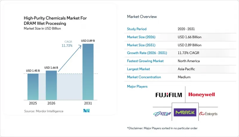
Mordor Intelligence에 의하면, DRAM 습식 공정용 고순도 화학제품 시장 규모는 2025년 14억 5,000만 달러로 평가되었습니다. 2026년에는 16억 6,000만 달러로 확대되어 2031년까지 28억 9,000만 달러에 이를 것으로 예상되고 2026년부터 2031년에 걸쳐 CAGR 11.73%로 성장할 전망입니다.

본 보고서는 화학 물질 유형(산, 염기, 용매 등), 공정 용도(웨이퍼 세정, 포토레지스트 박리 등), 순도 등급(SEMI 등급 5(첨단 DRAM 노드), SEMI 등급 4(성숙 DRAM 노드) 등), DRAM 제품 유형(DDR5 DRAM, HBM DRAM, DDR4 DRAM 등) 및 지역별로 분류되어 있습니다. 시장 전망은 금액(달러) 기준으로 제시되어 있습니다.
DRAM 습식 공정용 고순도 화학제품 시장 인사이트 및 동향
DRAM 노드의 미세화가 진행됨에 따라 습식 세정 빈도 증가
DRAM 노드의 미세화가 진행될 때마다 웨이퍼 1장당 습식 세정 공정이 증가할 뿐만 아니라, 순도 목표도 더욱 엄격해짐에 따라 DRAM 습식 공정용 고순도 화학제품 시장의 화학제품에 대한 지속적인 수요는 계속 증가하고 있습니다. N90부터 A14에 이르는 공정 노드를 대상으로 한 조사에 따르면, 습식 공정은 전체 기술 흐름에서 화학제품 총 소비량의 35-59%를 차지하고 있으며, 첨단 미세화 공정에서도 여전히 화학제품 사용량의 대부분을 차지하는 부분입니다. 이러한 추세는 웨이퍼 생산 시작량이 완만하더라도 화학제품 수요가 계속 증가할 가능성이 있음을 의미합니다. 각 웨이퍼를 전체 공정에서 처리하기 위해서는 더 많은 화학제품이 필요하기 때문입니다. 또한, 1-베타 및 1-감마 구조로의 전환에 따라 박막 형성, 선택적 에칭, 잔류물 제거 공정이 추가되어 필요한 세정 사이클의 수도 증가합니다. SEMI C1에 기반한 액체 화학제품 인증에 사용되는 분석 프레임워크를 이미 충족하고 있는 공급업체는 고객이 세대별로 화학제품 재인증을 진행하는 과정에서 기존 입지를 지키기 쉬운 위치에 있습니다. 이로 인해 DRAM 습식 공정을 위한 고순도 화학 약품 시장은 단순한 생산량뿐만 아니라 기술 전환 및 수율 관리와 밀접하게 연계된 상태를 유지하고 있습니다.
고대역폭 메모리(HBM)의 확대가 첨단 표면 처리 수요를 견인
HBM은 TSV 형성, 층간 결합 및 에칭 후 세정 과정에서 기존 평면형 메모리 공정보다 더 엄격한 표면 제어가 요구되기 때문에 화학제품 사용량이 가장 많은 DRAM 형식 중 하나입니다. 애플라이드 머티리얼즈(Applied Materials)에 따르면, HBM의 생산량은 최근 몇 년간 연평균 성장률(CAGR) 약 50%로 증가하고 있으며, 이러한 성장세가 첨단 DRAM 웨이퍼 가공 및 관련 소재 기술에 대한 견고한 수요를 뒷받침하고 있습니다. TSV의 치수가 미세화되고 종횡비가 높아짐에 따라 잔류물 제거는 더욱 정교해져야 하며, 입자나 미량 오염 물질에 대한 허용 범위는 좁아지고 있습니다. 이로 인해, 특히 TSV 형성 후 및 본딩 전 표면 처리 공정에서 등급 요건과 웨이퍼당 화학제품 소비량이 모두 증가하고 있습니다. DRAM 습식 공정을 위한 고순도 화학제품 시장에서 HBM이 중요시되는 이유는 그 급속한 성장뿐만 아니라, 수익을 고부가가치 제제로 전환시키는 점에도 있습니다. 따라서 하이브리드 본딩 및 첨단 표면 처리에 특화된 화학 약품을 취급하는 공급업체는 기존의 DDR 공정에만 주력하는 공급업체보다 더 많은 가치를 창출할 수 있는 위치에 있습니다.
초고순도 인증 절차가 신규 공급업체 시장 진입을 지연시키고 있습니다.
최종 수요가 견조함에도 불구하고, 초고순도 인증 절차가 DRAM 습식 공정용 고순도 화학제품 시장에 신규 공급업체의 진입을 지연시키고 있습니다. 최첨단 DRAM 팹에서는 분석 검증, 공정 적합성 시험 및 수율에 미치는 영향 평가를 통해 전자 등급 액체 화학 약품의 경우 인증에 12-18개월이 소요되며, 신규 제제의 경우 이 기간이 더욱 길어질 가능성이 있습니다. SEMI F115 규격에 따라 이러한 부담은 액체 자체에 그치지 않고, 공급 시스템 및 구성 부품 전체의 액체 접촉면도 금속 오염 관련 요건을 충족해야 합니다. 특정 공정 단계에서 공급업체가 승인되면, 변경을 실시할 경우 수율, 장비 성능, 혹은 장기적인 생산 안정성에 악영향을 미칠 가능성이 있으므로 전환 비용이 높아집니다. 이로 인해 기존 공급업체는 여러 노드 세대에 걸쳐 입지를 지킬 수 있으며, 일반적인 산업용 화학제품 시장에 비해 단독 공급처와의 관계가 더욱 공고해집니다. 이익률을 지키기 위한 이러한 장벽은 DRAM 습식 공정을 위한 고순도 화학제품 시장에서 신규 생산 능력 확대가 공급업체 선택의 폭을 넓히는 속도를 둔화시키는 요인이 되고 있습니다.
부문 분석
2025년, DRAM 습식 공정을 위한 고순도 화학제품 시장에서 산은 41.26%의 점유율을 차지하며, DRAM의 습식 세정 및 에칭 공정 전반에 걸쳐 핵심적인 역할을 수행하고 있는 것으로 확인되었습니다. 불화수소산, H₃PO₄ 및 H₂SO₄는 웨이퍼 공정 전반에 걸쳐 반복적으로 수행되는 네이티브 산화막 제거, 선택적 에칭 및 스트립 관련 공정 단계에서 계속해서 기본적인 원료로 사용되고 있습니다. 따라서 디바이스 아키텍처가 세대마다 변화하더라도, 산은 DRAM 습식 공정을 위한 고순도 화학제품 시장에서 중심적인 위치를 계속 차지하고 있습니다. 또한, 이러한 우위는 습식 공정의 누적적인 특성도 반영하고 있습니다. 즉, 웨이퍼가 최종 제품이 되기까지 산에 의존하는 많은 공정을 거치기 때문입니다. 따라서 불소계 소재의 원료 공급이 부족한 상황에서는 공급업체의 이익률이 압박을 받더라도 산의 가치 상승을 뒷받침하는 요인이 될 수 있습니다.
산화제 및 세정제는 2031년까지 연평균 성장률(CAGR) 12.64%를 나타낼 것으로 예측되며, DRAM 습식 공정을 위한 고순도 화학제품 시장에서 가장 빠르게 성장하는 화학제품 그룹이 될 것입니다. 미세화가 진행됨에 따라 잔류물에 대한 민감도가 높아지고 있어, 최첨단 DRAM 제조 라인에서는 황산·과산화수소 혼합액, 오존 처리된 탈이온수 및 고순도 과산화수소의 사용이 증가하고 있습니다. 솔베이(Solvay)에 따르면, 이 회사의 전자 등급 과산화수소(H2O2) 사업은 2025년 9월에 완공된 진장(Zhenjiang) 공장의 생산 능력 배가에 힘입어 판매량에서 두 자릿수 성장을 달성했습니다. 염기나 용매도 여전히 중요하지만, 팹이 고도의 스트리핑 및 표면 처리를 위해 오존 보조형 또는 수성 산화제 공정으로 전환함에 따라 용매 시장은 더 큰 구조적 압박에 직면하고 있습니다.
2025년 매출에서 웨이퍼 세정이 차지하는 비중은 48.72%에 달하여, DRAM 습식 공정을 위한 고순도 화학제품 시장에서 가장 큰 용도로 자리매김했습니다. 이 규모는 DRAM 노드가 복잡해짐에 따라 증가하는 게이트 형성 전, CMP 후, 에칭 후 및 층간 세정의 누적 비중을 반영합니다. 피어 리뷰를 거친 연구에 따르면, 습식 공정은 여러 노드 세대에 걸쳐 화학 약품의 주요 용도로 계속 유지되어 왔으며, 이는 총 소비량에서 세정이 차지하는 큰 비중을 뒷받침합니다. 또한, 첨단 셀 구조는 여전히 선택적 제거 및 결함에 민감한 계면에 의존하고 있기 때문에 프런트엔드 표면 처리 및 습식 에칭도 중요한 역할을 유지하고 있습니다. 이 때문에 DRAM 습식 공정을 위한 고순도 화학제품 시장은 단일 공정 단계라기보다는 오염 방지에 중점을 둔 형태로 자리 잡고 있습니다.
포토레지스트 박리는 2031년까지 연평균 성장률(CAGR) 12.78%로 확대될 것으로 예상되며, 이는 DRAM 습식 공정을 위한 고순도 화학제품 시장의 공정 용도 중 가장 빠른 성장 속도를 보일 것입니다. EUV 관련 패터닝으로 인해 웨이퍼당 레지스트 제거 사이클 수가 증가함에 따라, 산, 산화제 및 특수 박리용 화학제품에 대한 수요가 높아지고 있습니다. CMP 후의 세정 및 표면 처리는 총량으로는 여전히 소규모이지만, 섬세한 유전체 층을 손상시키지 않고 잔류물을 제거해야 한다는 점에서 기술적으로 차별화되어 있습니다. 따라서 DRAM 습식 공정용 고순도 화학제품 업계에서 취급량이 웨이퍼 세정을 밑돌더라도 독자적인 배합의 약제가 중요한 역할을 하고 있습니다.
지역별 분석
2025년에는 아시아태평양이 매출의 87.53%를 차지하며, DRAM 습식 공정용 고순도 화학제품 시장의 중심지로서의 위치를 유지했습니다. 이러한 집중 현상은 한국, 대만, 일본, 중국에 위치한 주요 DRAM 생산 거점의 입지를 반영한 것입니다. 한국은 Samsung Electronics 및 SK하이닉스가 최첨단 DRAM 생산을 가장 집중적으로 수행하고 있었기 때문에 계속해서 핵심적인 수요 기반이 되었습니다. 대만은 난야 테크놀로지(NANYA Technology)와 마이크론(Micron)의 사업을 통해 2차 성장층을 형성했으며, 일본은 소비 거점인 동시에 특수 화학제품 수출업체를 위한 공급 거점 역할도 수행했습니다. 그 결과, 아시아태평양의 DRAM 습식 공정용 고순도 화학제품 시장은 팹, 정제 인프라, 수출 역량이 긴밀하게 연계된 지역 클러스터로 통합되었습니다.
북미는 2031년까지 연평균 성장률(CAGR) 12.93%를 나타낼 것으로 예측되며, DRAM 습식 공정을 위한 고순도 화학제품 시장에서 가장 빠르게 성장하는 지역이 될 전망입니다. NIST에 따르면, ‘CHIPS for America’에는 반도체 제조 시설에 대한 390억 달러 규모의 지원이 포함되어 있어, 이를 통해 업스트림 소재 및 공급망에 대한 투자를 미국으로 유치하는 데 기여하고 있습니다. 각 습식 화학 약품은 대량 사용에 앞서 여전히 완벽한 순도와 공정 인증이 필요하기 때문에 이로 인해 아시아에 대한 의존도가 급격히 줄어들지는 않을 것입니다. 그럼에도 불구하고, 미국 내 새로운 팹 및 패키징 생산 능력의 확장은 현지에서의 정제, 혼합, 물류 지원의 여지를 만들어내고 있습니다. 유럽의 DRAM에 대한 직접적인 수요는 여전히 소규모에 그치고 있지만, BASF가 루트비히스하펜에서 반도체 등급 황산 및 전자 등급 수산화암모늄에 투자한 것은 더 광범위한 반도체 분야에 대한 야망과 더불어 현지 습식 화학제품 공급 역량이 구축되고 있음을 보여줍니다.
세계 기타 지역에서는 DRAM 습식 공정을 위한 고순도 화학제품 시장의 절대적인 매출액이 여전히 소규모에 그쳤습니다. 동남아시아는 최첨단 DRAM 제조 거점이라기보다는 물류, 조립, 유통의 거점으로서 더 중요한 역할을 수행하고 있었습니다. 중동은 불소계 원료의 중계지로서 전략적으로 중요하며, 해당 지역에서 혼란이 발생하면 전 세계 소재 공급 상황에 파급될 우려가 있었습니다. 남미는 첨단 메모리 제조 공장 인프라가 부족했기 때문에 예측 기간 동안 여전히 무시할 수 있을 정도의 기여도에 그쳤습니다.
기타 혜택 :
- 엑셀 형식 시장 예측(ME) 시트
- 3개월간의 애널리스트 지원
자주 묻는 질문
목차
제1장 서론
제2장 조사 방법
제3장 주요 요약
제4장 시장 구도
제5장 시장 규모 및 성장 예측
제6장 경쟁 구도
제7장 시장 기회 및 향후 전망
KTH 26.08.10According to Mordor Intelligence, the high-purity chemicals market for DRAM wet processing size is expected to increase from USD 1.45 billion in 2025 to USD 1.66 billion in 2026 and reach USD 2.89 billion by 2031, growing at a CAGR of 11.73% over 2026-2031.
This report is Segmented by Chemical Type (Acids, Bases, Solvents, and More), Process Application (Wafer Cleaning, Photoresist Stripping, and More), Purity Grade (SEMI Grade 5 [Advanced DRAM Nodes], SEMI Grade 4 [Mature DRAM Nodes], and More), DRAM Product Type (DDR5 DRAM, HBM DRAM, DDR4 DRAM, and More), and Geography. The Market Forecasts are Provided in Terms of Value (USD).
Insights and Trends of High-Purity Chemicals Market For DRAM Wet Processing
Rising DRAM Node Shrinks Increasing Wet Clean Intensity
Each new DRAM node shrink adds more wet clean steps per wafer, not just tighter purity targets, which keeps recurring chemical demand rising in the high-purity chemicals market for DRAM wet processing. Research covering process nodes from N90 to A14 showed that wet processing accounted for 35-59% of total chemical consumption across a full technology flow, and it remained the dominant chemical-use block even at advanced geometries. That pattern means chemical demand can keep rising even when wafer start growth is moderate, because more chemistry is needed to process each wafer through the full sequence. The move to 1-beta and 1-gamma structures also adds deposition, selective etch, and residue-removal steps, increasing the number of required clean cycles. Suppliers that already meet the analytical framework used for liquid chemical qualification under SEMI C1 are better placed to defend incumbency as customers requalify chemicals generation by generation. This keeps the high-purity chemicals market for DRAM wet processing tied to technology migration and yield control, rather than just unit output.
High Bandwidth Memory Expansion Driving Advanced Surface Preparation Demand
HBM is one of the most chemically intensive DRAM formats because TSV formation, layer bonding, and post-etch cleaning require tighter surface control than conventional planar memory flows. Applied Materials said HBM output has been growing at roughly a 50% CAGR in recent years, a pace that is supporting healthy demand for advanced DRAM wafer processing and related materials capabilities. As TSV dimensions shrink and aspect ratios rise, residue removal becomes more sensitive, and the tolerance for particles and trace contaminants narrows. That raises both grade requirements and unit chemical consumption per wafer, especially in post-TSV and bonding surface preparation steps. In the high-purity chemicals market for DRAM wet processing, HBM matters not only because it is growing quickly, but also because it shifts revenue toward higher-value formulations. Suppliers with dedicated chemistries for hybrid bonding and advanced surface conditioning, therefore, stand to capture more value than suppliers focused only on conventional DDR flows.
Ultra-High Purity Qualification Cycles Slowing New Supplier Entry
Ultra-high-purity qualification cycles are slowing new supplier entry into the high-purity chemicals market for DRAM wet processing, even as end demand remains strong. At leading-edge DRAM fabs, analytical verification, process compatibility testing, and yield-impact review can stretch qualification to 12-18 months for electronic-grade liquids and longer for new formulations. SEMI F115 extends this burden beyond the liquid itself, as wetted surfaces across delivery systems and components must also meet the metallic contamination requirements. Once a supplier is approved at a specific process step, switching costs become high because any change can disturb yield, tool performance, or long-cycle production stability. This helps incumbents defend their positions through multiple node generations and makes sole-source relationships more durable than in broader industrial chemical markets. The same barrier that protects margins also slows the pace at which new capacity translates into broader supplier choice inside the high-purity chemicals market for DRAM wet processing.
Other drivers and restraints analyzed in the detailed report include:
- Tight Contamination Limits at Sub-PPTrillion Levels Raising Chemical Consumption Per Wafer
- Fab Localization Incentives Expanding Qualified Chemical Buying across New Capacity
- High Cost of Electronic-Grade Purification, Packaging, and Analytical Control
For complete list of drivers and restraints, kindly check the Table Of Contents.
Segment Analysis
Acids accounted for 41.26% of the high-purity chemicals market for DRAM wet processing share in 2025, confirming their central role across DRAM wet clean and etch sequences. Hydrofluoric acid, H3PO4, and H2SO4 remain basic inputs for native oxide removal, selective etch, and strip-related process steps that appear repeatedly across a wafer flow. This keeps acids at the core of the high-purity chemicals market for DRAM wet processing even as device architecture changes from one generation to the next. Their lead also reflects the cumulative nature of wet processing, as a wafer moves through many acid-dependent operations before reaching the final output. Feedstock tightness in fluorinated materials can therefore support growth in acid value even when supplier margins are under pressure.
Oxidizers and cleaning agents are projected to grow at a 12.64% CAGR through 2031, making them the fastest-rising chemical group in the high-purity chemicals market for DRAM wet processing. Advanced DRAM lines are using more sulfuric-peroxide mixtures, ozonated DI water, and high-purity hydrogen peroxide as residue sensitivity rises at smaller geometries. Solvay said its electronic-grade H2O2 business delivered double-digit volume growth, supported by a capacity doubling at its Zhenjiang facility completed in September 2025. Bases and solvents still matter, but solvents face more structural pressure where fabs move toward ozone-assisted or aqueous oxidant sequences for advanced stripping and surface preparation.
Wafer cleaning accounted for 48.72% of revenue in 2025, making it the largest application in the high-purity chemicals market for DRAM wet processing. Its scale reflects the cumulative weight of pre-gate, post-CMP, post-etch, and inter-level cleans that multiply as DRAM nodes become more complex. A peer-reviewed study found that wet processing remained the dominant chemical use across multiple node generations, supporting the large share of cleaning in total consumption. Front-end surface preparation and wet etching also maintained significant roles because advanced cell structures still depend on selective removal and defect-sensitive interfaces. This leaves the high-purity chemicals market for DRAM wet processing tilted toward contamination prevention rather than toward one-time process events.
Photoresist stripping is projected to expand at a 12.78% CAGR through 2031, the fastest pace among process applications in the high-purity chemicals market for DRAM wet processing. EUV-related patterning increases the number of resist-removal cycles per wafer, thereby increasing demand for acids, oxidizers, and specialized strip chemistries. Post-CMP cleaning and surface conditioning remain smaller in total volume, but they are technically differentiated because they must remove residue without damaging delicate dielectric layers. That gives proprietary formulations a premium role even when their volume stays below wafer cleaning inside the high-purity chemicals for DRAM wet processing industry.
Complete Report Scope:
- By Chemical Type
- Acids
- Bases
- Solvents
- Oxidizers and Cleaning Agents
- By Process Application
- Wafer Cleaning
- Front-End Surface Preparation
- Wet Etching
- Photoresist Stripping
- Other Process Applications
- By Purity Grade
- SEMI Grade 5 (Advanced DRAM nodes)
- SEMI Grade 4 (Mature DRAM nodes)
- Higher Emerging UHP Grades / Customized Purity Formulations
- By DRAM Product Type
- DDR5 DRAM
- LPDDR5 / LPDDR5X DRAM
- HBM DRAM
- DDR4 DRAM
- Specialty and Embedded DRAM
- By Geography
- North America
- Europe
- Asia-Pacific
- China
- Japan
- South Korea
- Taiwan
- Rest of Asia-Pacific
- Rest of the World
Geography Analysis
Asia-Pacific accounted for 87.53% of revenue in 2025, thereby remaining the center of the high-purity chemicals market for DRAM wet processing. That concentration reflected the location of major DRAM production in South Korea, Taiwan, Japan, and China. South Korea remained the core demand base because Samsung Electronics and SK Hynix operated the highest concentration of advanced DRAM output. Taiwan added a secondary growth layer through NANYA Technology and Micron operations, while Japan served as both a consumption base and a supply base for specialty chemical exporters. As a result, the high-purity chemicals market for DRAM wet processing in Asia-Pacific combined fabs, purification infrastructure, and export capabilities into a tightly linked regional cluster.
North America is projected to grow at a 12.93% CAGR through 2031, making it the fastest-growing regional slice of the high-purity chemicals market for DRAM wet processing. NIST said CHIPS for America included USD 39 billion in support for semiconductor manufacturing facilities, helping attract upstream materials and supply-chain investment into the United States. This does not reduce Asian dependence quickly, as each wet chemical still requires full purity and process qualification before high-volume use. Even so, new fab and packaging capacity in the United States is opening space for local purification, blending, and logistics support. Europe remained smaller in direct DRAM demand, but BASF's semiconductor-grade sulfuric acid and electronic-grade ammonium hydroxide investments in Ludwigshafen showed that local wet chemical supply capability was being built alongside broader semiconductor ambitions.
Rest of the World remained modest in absolute revenue within the high-purity chemicals market for DRAM wet processing. Southeast Asia was more relevant as a logistics, assembly, and distribution layer than as a leading-edge DRAM manufacturing base. The Middle East mattered strategically as a transit corridor for fluorinated feedstocks, which meant disruption there could ripple into global material availability. South America remained a negligible contributor during the forecast window because it lacked advanced memory fab infrastructure.
- Entegris, Inc.
- Stella Chemifa Corporation
- Merck KGaA
- FUJIFILM Corporation
- Honeywell International Inc.
- BASF SE
- Dow Inc.
- Solvay S.A.
- Tokyo Ohka Kogyo Co., Ltd.
- JSR Corporation
- Shin-Etsu Chemical Co., Ltd.
- Sumitomo Chemical Co., Ltd.
- Mitsubishi Chemical Group Corporation
- Air Liquide S.A.
- Linde plc
- Avantor, Inc.
- Eastman Chemical Company
- Capchem Technology Co., Ltd.
Additional Benefits:
- The market estimate (ME) sheet in Excel format
- 3 months of analyst support
TABLE OF CONTENTS
1 INTRODUCTION
- 1.1 Study Assumptions and Market Definition
- 1.2 Scope of the Study
2 RESEARCH METHODOLOGY
3 EXECUTIVE SUMMARY
4 MARKET LANDSCAPE
- 4.1 Market Overview
- 4.2 Market Drivers
- 4.2.1 Rising DRAM Node Shrinks Increasing Wet Clean Intensity
- 4.2.2 High Bandwidth Memory Expansion Driving Advanced Surface Preparation Demand
- 4.2.3 Fab Localization Incentives Expanding Qualified Chemical Buying Across New Capacity
- 4.2.4 Tight Contamination Limits at Sub-PPTrillion Levels Raising Chemical Consumption per Wafer
- 4.2.5 Dual Sourcing Requirements Favoring Suppliers With Multi-Region Purification Assets
- 4.2.6 On-Site Chemical Blending and Packaging Integration Lowering Defect Risk in Wet Processing
- 4.3 Market Restraints
- 4.3.1 Ultra-High Purity Qualification Cycles Slowing New Supplier Entry
- 4.3.2 High Cost of Electronic-Grade Purification, Packaging, and Analytical Control
- 4.3.3 Regional Feedstock Concentration for Fluorinated and Oxidizing Inputs
- 4.3.4 Water, Waste, and Emissions Compliance Burden on Wet Chemical Producers
- 4.4 Industry Value Chain Analysis
- 4.5 Regulatory Landscape
- 4.6 Technological Outlook
- 4.7 Impact of Macroeconomic Factors on the Market
- 4.8 Porter's Five Forces Analysis
- 4.8.1 Threat of New Entrants
- 4.8.2 Bargaining Power of Buyers
- 4.8.3 Bargaining Power of Suppliers
- 4.8.4 Threat of Substitutes
- 4.8.5 Industry Rivalry
5 MARKET SIZE AND GROWTH FORECASTS (VALUE)
- 5.1 By Chemical Type
- 5.1.1 Acids
- 5.1.2 Bases
- 5.1.3 Solvents
- 5.1.4 Oxidizers and Cleaning Agents
- 5.2 By Process Application
- 5.2.1 Wafer Cleaning
- 5.2.2 Front-End Surface Preparation
- 5.2.3 Wet Etching
- 5.2.4 Photoresist Stripping
- 5.2.5 Other Process Applications
- 5.3 By Purity Grade
- 5.3.1 SEMI Grade 5 (Advanced DRAM nodes)
- 5.3.2 SEMI Grade 4 (Mature DRAM nodes)
- 5.3.3 Higher Emerging UHP Grades / Customized Purity Formulations
- 5.4 By DRAM Product Type
- 5.4.1 DDR5 DRAM
- 5.4.2 LPDDR5 / LPDDR5X DRAM
- 5.4.3 HBM DRAM
- 5.4.4 DDR4 DRAM
- 5.4.5 Specialty and Embedded DRAM
- 5.5 By Geography
- 5.5.1 North America
- 5.5.2 Europe
- 5.5.3 Asia-Pacific
- 5.5.3.1 China
- 5.5.3.2 Japan
- 5.5.3.3 South Korea
- 5.5.3.4 Taiwan
- 5.5.3.5 Rest of Asia-Pacific
- 5.5.4 Rest of the World
6 COMPETITIVE LANDSCAPE
- 6.1 Market Concentration
- 6.2 Strategic Moves
- 6.3 Market Share Analysis
- 6.4 Company Profiles (includes Global Level Overview, Market Level Overview, Core Segments, Financials as available, Strategic Information, Market Rank/Share, Products and Services, Recent Developments)
- 6.4.1 Entegris, Inc.
- 6.4.2 Stella Chemifa Corporation
- 6.4.3 Merck KGaA
- 6.4.4 FUJIFILM Corporation
- 6.4.5 Honeywell International Inc.
- 6.4.6 BASF SE
- 6.4.7 Dow Inc.
- 6.4.8 Solvay S.A.
- 6.4.9 Tokyo Ohka Kogyo Co., Ltd.
- 6.4.10 JSR Corporation
- 6.4.11 Shin-Etsu Chemical Co., Ltd.
- 6.4.12 Sumitomo Chemical Co., Ltd.
- 6.4.13 Mitsubishi Chemical Group Corporation
- 6.4.14 Air Liquide S.A.
- 6.4.15 Linde plc
- 6.4.16 Avantor, Inc.
- 6.4.17 Eastman Chemical Company
- 6.4.18 Capchem Technology Co., Ltd.
7 MARKET OPPORTUNITIES AND FUTURE OUTLOOK
- 7.1 White-Space and Unmet-Need Assessment


