

|
시장보고서
상품코드
2100018
항공우주 및 방위용 반도체 소자 시장 : 점유율 분석, 업계 동향 및 통계, 성장 예측(2026-2031년)Semiconductor Device in Aerospace and Defense Industry - Market Share Analysis, Industry Trends & Statistics, Growth Forecasts (2026 - 2031) |
||||||
 Mordor Intelligence
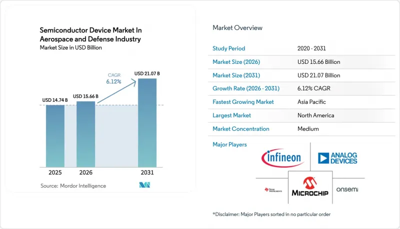
Mordor Intelligence에 의하면, 항공우주 및 방위용 반도체 소자 시장 규모는 2025년 147억 4,000만 달러에서 2026년에는 156억 6,000만 달러로 확대되어 2031년까지 210억 7,000만 달러에 이를 것으로 예상되고 있어 2026년부터 2031년까지 CAGR 6.12%로 성장할 전망입니다.
본 보고서는 소자 유형(디스크리트 반도체, 광전자 등), 소재(실리콘, 실리콘 카바이드, 갈륨 나이탈리아드 등), 용도(통신·데이터 처리, 레이더·ISR 등), 최종 용도 플랫폼(민간 항공, 군용 항공 등), 지역별로 분류되어 있습니다. 시장 전망은 금액(달러) 기준으로 제시되어 있습니다.
항공우주 및 방위용 반도체 소자 시장 동향과 전망
차세대 군사·우주용 전원 시스템에서 광대역 갭(SiC 및 GaN) 디바이스의 채택이 급증
SiC 및 GaN 소자는 실리콘에 비해 내전압이 높고, 스위칭 속도가 빠르며, 방열 효율도 뛰어나기 때문에 미사일이나 위성의 전원 장치를 경량화할 수 있게 합니다. Wolfspeed사는 미국 공군의 차세대 전투기용으로 1,700V SiC MOSFET 인증을 획득하여 컨버터의 질량을 30% 줄였습니다. 유럽우주국(ESA)은 1kW 태양전지 레귤레이터의 질량을 40% 줄인 GaN-on-silicon 파워 IC를 채택했습니다. 노스롭 그루먼사는 AESA 레이더용 SiC 공급을 확보하기 위해 장기 웨이퍼 구매 계약을 체결하며, 전략적인 선제 조달 자세를 강조했습니다. Qorvo사는 초음속 무기를 주요 견인 요인으로 꼽으며, 2023년부터 2025년까지 방위 분야 매출에서 GaN 증폭기가 차지하는 비중이 11%에서 18%로 상승할 것이라고 보고했습니다. 또한 SiC는 실리콘에 비해 열전도율이 3배 높기 때문에 중량이 중요한 항공기 탑재 페이로드에서 방열판의 크기를 축소하는 것도 가능합니다.
LEO 위성의 메가 콘스텔레이션이 내방사선성 RFIC 수요를 견인
메가 콘스텔레이션에서는 상용 가격대의 내방사선성이 요구되고 있습니다. 2025년에 발사될 Starlink Gen2 위성은 1기당 1,200개 이상의 GaN RFIC를 탑재하고 있어, 총 이온화 선량(TID) 내성을 갖춘 제품에 대한 수요를 비약적으로 증가시키고 있습니다. 아마존의 Project Kuiper에서는 300 krad의 방사선을 견디면서 소비 전력을 절반으로 줄이는 RTG4 기반 FPGA에 대해 Microchip Technology에 계약이 수주되었습니다. OneWeb의 사업 재개에 따라 Teledyne e2v의 웨이퍼 시작 건수가 35% 증가하면서, 90nm 이하 공정에서공급 부족이 두드러지게 나타났습니다. 미국 우주군의 트랜치 2(Tranche 2) 위성에는 Versal AI Core FPGA에 AI 라우팅 기능이 통합되어 있어, ‘실용적으로 충분한’ 내방사선성에 대한 수용이 더욱 강화되고 있습니다. 기존 공급업체들은 가격 경쟁력을 유지하기 위해 현재 상용 파운드리 업체에 제조 라이선스를 부여하고 있습니다.
90nm 이하 방사선 내성 파운드리 생산 능력은 제한적입니다.
90nm 이하의 양산용 내방사선 공정을 가동하고 있는 곳은 BAE 시스템즈의 뉴햄프셔 공장과 타워 세미컨덕터의 뉴포트비치 거점뿐이며, 두 공장 모두 가동률이 95%를 초과하고 있습니다. RTG4 FPGA의 리드타임은 2025년에는 52주에 달할 전망입니다. 새로운 내방사선 라인의 인증에는 최대 8,000만 달러와 3년이 소요되기 때문에 신규 진입을 가로막고 있습니다. 텔레다인 e2v는 65nm 공정의 생산 할당량이 ESA 임무로 이미 채워져 있었기 때문에 4,000만 유로 규모의 수주를 거절할 수밖에 없었습니다. 그 결과, 설계자들은 집적도와 전력 소비 간의 절충점을 수용하면서 180nm 공정으로 되돌아가고 있습니다.
부문 분석
집적 회로는 2025년 ‘항공우주 및 방위용 반도체 소자 시장’ 규모에서 44.61%를 차지하며, 항공 전자 장비 및 페이로드용 프로세서, FPGA, 그리고 혼합 신호 프런트엔드를 공급하고 있습니다. 광전자 분야는 규모는 작지만, LiDAR 탑재 무기나 위성 간 광 링크의 보급에 따라 연평균 성장률(CAGR) 8.13%로 다른 분야를 상회하는 성장이 예상됩니다. 레이시온(Raytheon)사의 ‘StormBreaker’는 레이저 조준용으로 인듐·갈륨·비소(IGAr) 광검출기를 채택하고 있습니다. 나머지 분야는 디스크리트 파워 디바이스와 센서가 차지하고 있으며, 차세대 드론에 탑재되는 하이퍼스펙트럼 이미저에 의해 그 수요가 가속화되고 있습니다.
광전자공학의 성장은 구조적인 것입니다. 광 링크는 초당 기가비트 단위의 데이터를 전송하여 RF 혼잡을 피합니다. L3Harris사는 궤도상에서 18개월간 계속 작동한 레이저를 사용하여 2025년에 10 Gbps의 광 다운링크를 실현했습니다. 트럭 탑재형 레이저의 1700V 스위칭에는 여전히 디스크리트 SiC MOSFET가 필수적입니다. 하이브리드 패키징 기술을 통해 현재는 III-V계 레이저를 실리콘 CMOS 위에 마이크로프린팅하고 있으며, 20-30%의 비용 증가를 수반하면서도 폼 팩터를 소형화하고 있습니다.
실리콘은 공급 체계의 확충과 오랜 인증 실적을 바탕으로, 2025년 항공우주 및 방위용 반도체 소자 시장에서 62.13%의 점유율을 차지했습니다. 초음속기, 재머, 위상 배열 관련 프로그램이 GaAs의 한계를 넘어감에 따라, GaN 시장 점유율은 연평균 7.36%로 확대될 것으로 예측됩니다. 공군의 차세대 재머는 GaN 모듈만을 사용하여 6-18GHz 대역에서 1 kW의 출력을 방출합니다. SiC는 전력 변환에 사용되며, 150°C에서 98%의 효율을 달성할 수 있기 때문에 비용이 3-5배 더 비싸다는 점도 정당화되고 있습니다.
60GHz 이상의 밀리파 대역에서는 인듐 인화물이 주류를 이루고 있지만, 다이아몬드 기판은 비용이 높음에도 불구하고 GaN의 전력 밀도를 200 W/mm까지 높일 수 있습니다. Qorvo사는 다이아몬드 기판 위의 GaN에서 44GHz에서 150 W를 실현했습니다. 이는 SiC 기판 위의 GaN보다 50% 높은 출력, 웨이퍼 1장당 가격은 1만 달러를 초과합니다. GaN 팹을 SiC 기판 대응으로 전환하려면 약 2억 5,000만 달러의 설비 투자가 필요하기 때문에 진입할 수 있는 기업은 최대 규모 기업으로 한정됩니다.
지역별 분석
북미는 2025년에도 36.91%의 점유율을 유지했습니다. 이는 8,420억 달러 규모의 미국 국방 예산과 DARPA가 3D 패키징을 위해 시행하는 15억 달러 규모의 ‘전자 산업 부흥 이니셔티브(Electronics Resurgence Initiative)’에 힘입은 결과입니다. 'CHIPS 법'에는 390억 달러의 보조금이 책정되어 있으며, BAE 시스템즈는 뉴햄프셔주의 팹을 확장하여 웨이퍼 생산 능력을 25% 증강했습니다. 이 팹은 미국 내 유일하게 90nm 미만의 내방사선성 반도체를 공급하는 곳입니다. 캐나다 NORAD(북미항공우주방위사령부)의 업그레이드 계획에서는 MDA 스페이스사의 프로세서를 채택한 북극권 감시 위성을 위해 36억 달러가 배정되었습니다.
아시아태평양은 2031년까지 연평균 성장률(CAGR) 8.47%로 가장 높은 성장세를 보일 것으로 전망됩니다. 인도의 100억 달러 규모 반도체 미션에 따라 타워 세미컨덕터는 65nm 신뢰성 검증 완료 팹을 제안했습니다. 일본은 국산 내방사선성 F-3 프로세서 조달을 위해 미쓰비시 전기에 8억 달러를 발주했습니다. 한국은 삼성 파운드리와 제휴하여 KF-21의 미션 컴퓨터용으로 28nm FD-SOI 인증을 추진하고 있습니다. 중국의 CETC는 2025년에 28nm 내방사선 FPGA를 국내에서 생산하여 수입 의존도를 낮추겠다고 밝혔습니다. AUKUS 체제 하에서 추진되고 있는 호주의 35억 호주 달러 규모의 미사일·드론 계획은 국내 조립 수요를 뒷받침하고 있습니다.
유럽은 2030년까지 지역 점유율을 두 배로 늘리는 것을 목표로 하는 430억 유로 규모의 ‘EU 칩 법’에 주력하고 있습니다. ESA의 ‘ARIEL’ 및 ‘PLATO’ 임무는 SiC 및 방사선 내성 디바이스에 대한 수요를 뒷받침하고 있습니다. 독일의 23억 유로 규모 ‘타이푼’ 레이더 개량 프로젝트에서는 United Monolithic Semiconductors사의 GaN 모듈이 채택되었습니다. '템페스트' 전투기에서는 텍사스 기기(Texas Instruments) 및 NXP사의 FACE 준수 COTS 프로세서 사용이 의무화되어 있으며, 독자 개발 하드웨어에서 COTS로의 전환을 통해 업데이트 주기를 단축하고 있습니다.
기타 혜택:
- 엑셀 형식 시장 예측(ME) 시트
- 3개월간의 애널리스트 지원
자주 묻는 질문
목차
제1장 서론
제2장 조사 방법
제3장 주요 요약
제4장 시장 구도
제5장 시장 규모와 성장 예측
제6장 경쟁 구도
제7장 시장 기회와 향후 전망
JHS 26.08.11According to Mordor Intelligence, the semiconductor device market in the Aerospace and Defense Industry market size is expected to increase from USD 14.74 billion in 2025 to USD 15.66 billion in 2026 and reach USD 21.07 billion by 2031, growing at a CAGR of 6.12% over 2026-2031.
This report is Segmented by Device Type (Discrete Semiconductors, Optoelectronics, and More), Material (Silicon, Silicon Carbide, Gallium Nitride, and More), Application (Communication and Data Handling, Radar and ISR, and More), End-Use Platform (Commercial Aviation, Military Aviation, and More), and Geography. The Market Forecasts are Provided in Terms of Value (USD).
Insights and Trends of Semiconductor Device Market in Aerospace and Defense Industry
Surge in Wide-Bandgap (SiC and GaN) Adoption for Next-Gen Military and Space Power Systems
SiC and GaN devices tolerate higher voltages, switch faster, and dissipate heat more efficiently than silicon, enabling lighter power supplies in missiles and satellites. Wolfspeed qualified 1,700 V SiC MOSFETs for the U.S. Air Force's next-generation fighter, cutting converter mass by 30%. The European Space Agency selected GaN-on-silicon power ICs that reduced a 1 kW solar regulator's mass by 40%. Northrop Grumman executed long-term wafer purchases to secure SiC supply for AESA radars, underscoring its strategic forward purchasing. Qorvo reported GaN amplifiers rising from 11% to 18% of defense revenue between 2023 and 2025, driven by hypersonic weapons. SiC's three times higher thermal conductivity than silicon also reduces the size of heat sinks on weight-critical airborne payloads.
LEO Satellite Mega-Constellations Driving Radiation-Tolerant RFIC Demand
Mega-constellations demand radiation resilience at commercial price points. Starlink Gen2 satellites launched in 2025 carry more than 1 200 GaN RFICs each, multiplying total-ionizing-dose-hardened demand. Amazon's Project Kuiper awarded Microchip Technology a contract for RTG4-based FPGAs that survive 300 krad while halving power use. OneWeb's restart stretched wafer starts at Teledyne e2v by 35%, exposing sub-90 nm scarcity. The U.S. Space Force's Tranche 2 satellites embed AI routing on Versal AI Core FPGAs, reinforcing acceptance of "good-enough" rad tolerance. Traditional vendors now license commercial foundries to stay price-competitive.
Limited Rad-Hard Foundry Capacity Below 90 nm
Only BAE Systems' New Hampshire fab and Tower Semiconductor's Newport Beach site run volume rad-hard processes under 90 nm, both above 95% utilization. Lead times for RTG4 FPGAs stretched to 52 weeks in 2025. Qualifying a new rad-hard line costs up to USD 80 million and three years, discouraging entrants. Teledyne e2v even declined EUR 40 million orders as 65 nm slots were consumed by ESA missions. Designers therefore revert to 180 nm processes, accepting density and power trade-offs.
Other drivers and restraints analyzed in the detailed report include:
- Embedded AI Mission Computers in Multi-Domain Operations
- Hypersonic and Directed-Energy Programs Requiring Ultra-High-Frequency GaN RF Power Amplifiers
- Export-Control Tightening on Advanced Nodes
For complete list of drivers and restraints, kindly check the Table Of Contents.
Segment Analysis
Integrated circuits captured 44.61% of Semiconductor Device Market In Aerospace And Defense Industry market size in 2025, supplying processors, FPGAs, and mixed-signal front-ends for avionics and payloads. Optoelectronics, though smaller, will outpace others at 8.13% CAGR as LiDAR munitions and optical inter-satellite links spread. Raytheon's StormBreaker employs indium-gallium-arsenide photodetectors for laser targeting. Discrete power devices and sensors cover the remainder, accelerated by hyperspectral imagers on next-gen drones.
Optoelectronics' rise is structural. Optical links transmit gigabits per second and evade RF congestion. L3Harris achieved a 10 Gbps optical downlink in 2025 using lasers that survived 18 months on orbit. Discrete SiC MOSFETs stay vital for 1700 V switching in truck-mounted lasers. Hybrid packaging now micro-prints III-V lasers onto silicon CMOS, shrinking form factors at a 20-30% cost premium.
Silicon held 62.13% of Semiconductor Device Market In Aerospace And Defense Industry market share in 2025 thanks to supply depth and qualification heritage. GaN is projected to climb 7.36% annually as hypersonic, jammer, and phased-array programs exceed GaAs limits. The Air Force's next-gen jammer emits 1 kW across 6-18 GHz exclusively via GaN modules. SiC serves power conversion where 98% efficiency at 150 °C justifies its 3-5X cost premium.
Indium phosphide dominates millimeter-wave above 60 GHz; diamond substrates, though costly, enable 200 W/mm GaN densities. Qorvo showed 150 W at 44 GHz on GaN-on-diamond, 50% higher than GaN-on-SiC, though wafers exceed USD 10 000 each. Converting a GaN fab to SiC substrates needs about USD 250 million in tools, limiting participation to the largest players.
Complete Report Scope:
- By Device Type
- Discrete Semiconductors
- Optoelectronics
- Sensors
- Integrated Circuits
- By Material
- Silicon
- Silicon Carbide (SiC)
- Gallium Nitride (GaN)
- Others (GaAs, SiGe, InP, Diamond)
- By Application
- Communication and Data Handling
- Radar and ISR Payloads
- Navigation and Guidance
- Power Management and Propulsion Control
- Flight Control and Avionics
- Electronic Warfare and Counter-Measures
- Sensors and Scientific Payloads
- By End-Use Platform
- Commercial Aviation
- Military Aviation
- Spacecraft and Satellites
- Unmanned Aerial Vehicles (UAVs)
- Ground and Naval Defense Systems
- Missiles and Precision Munitions
- By Geography
- North America
- United States
- Canada
- Mexico
- South America
- Brazil
- Argentina
- Rest of South America
- Europe
- Germany
- United Kingdom
- France
- Italy
- Spain
- Rest of Europe
- Asia-Pacific
- China
- India
- Japan
- South Korea
- Australia and New Zealand
- Rest of Asia-Pacific
- Middle East
- Saudi Arabia
- United Arab Emirates
- Turkey
- Rest of Middle East
- Africa
- South Africa
- Nigeria
- Egypt
- Rest of Africa
- North America
Geography Analysis
North America retained 36.91% share in 2025, anchored by the USD 842 billion U.S. defense budget and DARPA's USD 1.5 billion Electronics Resurgence Initiative for 3D packaging. The CHIPS Act directs USD 39 billion in subsidies; BAE Systems expanded its New Hampshire fab by 25% wafer capacity, the nation's lone sub-90 nm rad-hard source. Canada's NORAD upgrade earmarks USD 3.6 billion for Arctic surveillance satellites using MDA Space processors.
Asia-Pacific will post the highest CAGR at 8.47% through 2031. India's USD 10 billion semiconductor mission drew Tower Semiconductor to propose a 65 nm trusted fab. Japan placed an USD 800 million order with Mitsubishi Electric for indigenous radiation-tolerant F-3 processors. South Korea partners Samsung Foundry to qualify 28 nm FD-SOI for the KF-21 mission computer. China's CETC produced 28 nm rad-hard FPGAs domestically in 2025, signaling reduced import reliance. Australia's AUD 3.5 billion missile-and-drone plan under AUKUS fuels demand for domestic assembly.
Europe relies on the EUR 43 billion EU Chips Act aiming to double regional share by 2030. ESA's ARIEL and PLATO missions sustain SiC and rad-tolerant demand. Germany's EUR 2.3 billion Typhoon radar upgrade uses GaN modules from United Monolithic Semiconductors. The Tempest fighter mandates FACE-compliant COTS processors from Texas Instruments and NXP, trading proprietary hardware for faster refresh.
- Analog Devices Inc.
- Microchip Technology Inc.
- Infineon Technologies AG
- onsemi (ON Semiconductor)
- Texas Instruments Inc.
- NXP Semiconductors N.V.
- STMicroelectronics N.V.
- Renesas Electronics Corp.
- Qorvo Inc.
- Wolfspeed Inc.
- Lattice Semiconductor Corp.
- Teledyne e2v (Teledyne Technologies)
- GSI Technology Inc.
- Cobham Advanced Electronic Solutions (CAES)
- BAE Systems plc (Microelectronics)
- Honeywell Aerospace Microelectronics
- Mercury Systems Inc.
- Broadcom Inc. (Rugged and Rad-Tolerant ASICs)
- Vorago Technologies
- L3Harris Technologies (Space Microelectronics)
- Airbus Defence and Space (HiRel ASIC Center)
Additional Benefits:
- The market estimate (ME) sheet in Excel format
- 3 months of analyst support
TABLE OF CONTENTS
1 INTRODUCTION
- 1.1 Study Assumptions and Market Definition
- 1.2 Scope of the Study
2 RESEARCH METHODOLOGY
3 EXECUTIVE SUMMARY
4 MARKET LANDSCAPE
- 4.1 Market Overview
- 4.2 Market Drivers
- 4.2.1 Surge in Wide-Bandgap (SiC and GaN) Adoption for Next-Gen Military and Space Power Systems
- 4.2.2 LEO Satellite Mega-Constellations Driving Radiation-Tolerant RFIC Demand
- 4.2.3 Embedded AI Mission Computers in Multi-Domain Operations (US and NATO)
- 4.2.4 Hypersonic and Directed-Energy Programs Requiring Ultra-High-Frequency GaN RF Power Amplifiers
- 4.2.5 Open-Architecture Avionics Refresh Cycles (FACE, MOSA) Expanding COTS IC Spend
- 4.2.6 Indigenous Fighter and UAV Platforms in Indo-Pacific Boosting Local Sourcing
- 4.3 Market Restraints
- 4.3.1 Limited Rad-Hard Foundry Capacity Below 90 nm
- 4.3.2 Export-Control Tightening on Advanced Nodes (US-China)
- 4.3.3 High QML-V and JANS Qualification Cost Burden
- 4.3.4 Thermal Management Limits in 3D-Packaged Space-Grade Chips
- 4.4 Industry Value-Chain Analysis
- 4.5 Regulatory Landscape
- 4.6 Technological Outlook
- 4.7 Porter's Five Forces Analysis
- 4.7.1 Bargaining Power of Buyers
- 4.7.2 Bargaining Power of Suppliers
- 4.7.3 Threat of New Entrants
- 4.7.4 Threat of Substitutes
- 4.7.5 Competitive Rivalry
5 MARKET SIZE AND GROWTH FORECASTS (VALUE)
- 5.1 By Device Type
- 5.1.1 Discrete Semiconductors
- 5.1.2 Optoelectronics
- 5.1.3 Sensors
- 5.1.4 Integrated Circuits
- 5.2 By Material
- 5.2.1 Silicon
- 5.2.2 Silicon Carbide (SiC)
- 5.2.3 Gallium Nitride (GaN)
- 5.2.4 Others (GaAs, SiGe, InP, Diamond)
- 5.3 By Application
- 5.3.1 Communication and Data Handling
- 5.3.2 Radar and ISR Payloads
- 5.3.3 Navigation and Guidance
- 5.3.4 Power Management and Propulsion Control
- 5.3.5 Flight Control and Avionics
- 5.3.6 Electronic Warfare and Counter-Measures
- 5.3.7 Sensors and Scientific Payloads
- 5.4 By End-Use Platform
- 5.4.1 Commercial Aviation
- 5.4.2 Military Aviation
- 5.4.3 Spacecraft and Satellites
- 5.4.4 Unmanned Aerial Vehicles (UAVs)
- 5.4.5 Ground and Naval Defense Systems
- 5.4.6 Missiles and Precision Munitions
- 5.5 By Geography
- 5.5.1 North America
- 5.5.1.1 United States
- 5.5.1.2 Canada
- 5.5.1.3 Mexico
- 5.5.2 South America
- 5.5.2.1 Brazil
- 5.5.2.2 Argentina
- 5.5.2.3 Rest of South America
- 5.5.3 Europe
- 5.5.3.1 Germany
- 5.5.3.2 United Kingdom
- 5.5.3.3 France
- 5.5.3.4 Italy
- 5.5.3.5 Spain
- 5.5.3.6 Rest of Europe
- 5.5.4 Asia-Pacific
- 5.5.4.1 China
- 5.5.4.2 India
- 5.5.4.3 Japan
- 5.5.4.4 South Korea
- 5.5.4.5 Australia and New Zealand
- 5.5.4.6 Rest of Asia-Pacific
- 5.5.5 Middle East
- 5.5.5.1 Saudi Arabia
- 5.5.5.2 United Arab Emirates
- 5.5.5.3 Turkey
- 5.5.5.4 Rest of Middle East
- 5.5.6 Africa
- 5.5.6.1 South Africa
- 5.5.6.2 Nigeria
- 5.5.6.3 Egypt
- 5.5.6.4 Rest of Africa
- 5.5.1 North America
6 COMPETITIVE LANDSCAPE
- 6.1 Market Concentration
- 6.2 Strategic Moves
- 6.3 Market Share Analysis
- 6.4 Company Profiles (includes Global Level Overview, Market Level Overview, Core Segments, Financials as available, Strategic Information, Market Rank/Share, Products and Services, Recent Developments)
- 6.4.1 Analog Devices Inc.
- 6.4.2 Microchip Technology Inc.
- 6.4.3 Infineon Technologies AG
- 6.4.4 onsemi (ON Semiconductor)
- 6.4.5 Texas Instruments Inc.
- 6.4.6 NXP Semiconductors N.V.
- 6.4.7 STMicroelectronics N.V.
- 6.4.8 Renesas Electronics Corp.
- 6.4.9 Qorvo Inc.
- 6.4.10 Wolfspeed Inc.
- 6.4.11 Lattice Semiconductor Corp.
- 6.4.12 Teledyne e2v (Teledyne Technologies)
- 6.4.13 GSI Technology Inc.
- 6.4.14 Cobham Advanced Electronic Solutions (CAES)
- 6.4.15 BAE Systems plc (Microelectronics)
- 6.4.16 Honeywell Aerospace Microelectronics
- 6.4.17 Mercury Systems Inc.
- 6.4.18 Broadcom Inc. (Rugged and Rad-Tolerant ASICs)
- 6.4.19 Vorago Technologies
- 6.4.20 L3Harris Technologies (Space Microelectronics)
- 6.4.21 Airbus Defence and Space (HiRel ASIC Center)
7 MARKET OPPORTUNITIES AND FUTURE OUTLOOK
- 7.1 White-Space and Unmet-Need Assessment


