|
시장보고서
상품코드
2121920
유럽의 이미지 센서 : 시장 점유율 분석, 업계 동향과 통계, 성장 예측(2026-2031년)Europe Image Sensors - Market Share Analysis, Industry Trends & Statistics, Growth Forecasts (2026 - 2031) |
||||||
 Mordor Intelligence
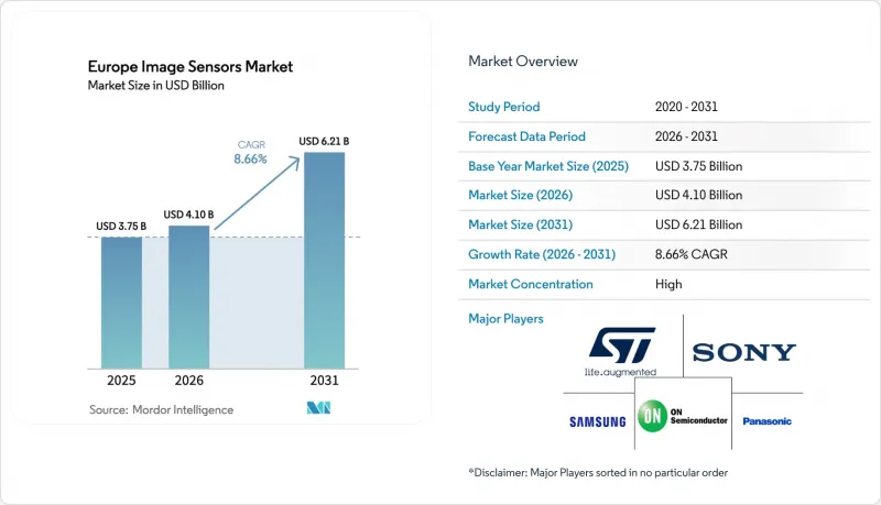
Mordor Intelligence에 따르면 유럽의 이미지 센서 시장 규모는 2025년에 37억 5,000만 달러, 2026년에 41억 달러에 달하며, 2031년까지 62억 1,000만 달러에 달할 것으로 예측되고 있으며, 2026-2031년에 CAGR 8.66%로 성장할 것으로 전망되고 있습니다.
이 보고서는 유형(CMOS, CCD), 해상도(8 MP 이하, 9-24 MP, 25-64 MP, 65-200 MP, 기타), 스펙트럼(가시광선(RGB), 근적외선(NIR), 단파장 적외선(SWIR), 기타),셔터 기술(롤링 셔터 CMOS, 글로벌 셔터 CMOS), 최종사용자 산업(소비자용 전자기기, 헬스케어, 산업, 기타) 및 지역별로 분류되어 있습니다. 시장 전망은 금액(달러) 기준으로 제시되어 있습니다.
유럽 이미지 센서 시장의 동향 및 인사이트
Euro NCAP의 전면 카메라 의무화(AEB)
Euro NCAP의 2025년 및 2026년 프로토콜에서는 운전자 모니터링 및 보행자 감지 성능에 대해 최대 25점이 부여되며, 5성급 평가를 목표로 하는 모든 자동차 제조사에 대해 근적외선 전방 및 차량 내부용 이미저의 채택이 사실상 의무화되었습니다. 각 시스템 통합사업자들은 2024년 7월 EU 일반 안전 규정(GSR) 시행 기한을 맞추기 위해 조달 일정을 18-24개월 앞당겼습니다. 이로 인해 유럽 이미지 센서 시장의 공급 수요가 더욱 높아졌습니다. onsemi는 2025년 3분기까지 자사의 자동차용 카메라 4억 5,000만 대가 이미 도로에서 가동 중이며, 그 설계 채택의 68%가 Euro 규격 준수 플랫폼과 관련되어 있다고 밝혔습니다. 또한 탑승자 분류에 관한 규제가 에어백 전개 기준을 엄격하게 하고 있으며, 규제에 따른 수요 증가가 비행시간법(ToF) 모듈의 조종석 도입을 촉진하고 있습니다. 독일의 Bosch, Continental, ZF는 의무화된 전면 카메라 영상과 측면 및 후면 영상을 융합하여, 기존 센서 공급업체를 보호하는 견고한 소프트웨어 인터페이스를 구축하고 있습니다. 따라서 이러한 의무화로 인해 차량당 탑재 대수가 증가함에 따라 기존 공급업체의 입지가 공고해졌으며, 이는 유럽 이미지 센서 시장의 성장 궤도에 크게 기여하고 있습니다.
2억 화소를 넘는 멀티 카메라 스마트폰 경쟁
2025년에는 소니와 옴니비전이 각각 2억 화소 센서를 발표했고, 플래그십 모델의 픽셀 피치가 0.6µm 아래로 떨어지면서 센서 1개당 평균 판매 가격은 30달러를 넘어섰습니다. 삼성은 프리미엄 시장에서의 입지를 되찾기 위해 화성에서 0.5µm 노드의 양산을 확대하고 있는 반면, 독일과 프랑스의 유럽 모듈 조립 제조사들은 서브미크론 픽셀이 더 엄격한 광학 공차를 필요로 하므로 생산량을 늘리고 있습니다. 웨이퍼 레벨 카메라 모듈은 렌즈를 다이 위에 직접 통합함으로써 Z 방향의 높이를 1.2 mm 줄여, 페리스코프식 망원 렌즈 설계를 가능하게 합니다. 아시아 칩 제조사들이 공급을 주도하고 있는 유럽의 이미지 센서 시장은 설비의 높은 자동화율과 유럽의 특수 유리 공급업체로부터 조달되는 포토닉 패키징 소재에 대한 수요 확대를 통해 간접적인 혜택을 보고 있습니다. 프리미엄 안드로이드 단말기의 출하 대수가 안정화되는 가운데, 매출 증가를 지원하는 것은 단순한 수량 확대가 아니라 부가가치의 향상입니다.
EU의 높은 에너지 비용과 클린룸의 공과금
유럽 대륙의 전기 요금은 동아시아의 2-3배에 달하는 높은 수준이며, 유럽의 이미지 센서 시장이 200mm에서 에너지 소비량이 많은 300mm 라인으로 전환되는 바로 그 시점에 제조 비용을 상승시키고 있습니다. 클린룸의 난방,환기, 공조 시스템은 팹 전체 에너지 소비량의 최대 40%를 차지하고 있으며, ST마이크로일렉트로닉스는 가격 변동에 대한 헤지 수단으로 부지내 태양광발전 및 열병합 발전에 1억 2,000만 유로(1억 2,800만 달러)를 투자할 수밖에 없는 상황입니다. KPMG의 2025년 반도체 조사에 따르면 이 지역 응답자의 66%가 에너지 전망의 불확실성을 이유로 설비 투자를 미루고 있으며, 이는 세계 평균인 51%를 크게 상회하는 수치입니다. ams-OSRAM의 5억 6,700만 유로(6억 200만 달러) 규모의 프레름슈테텐 프로젝트는 평균 판매 가격이 5달러를 초과하는 다품종 소량 생산 자동차 및 의료용 센서에 초점을 맞추고 있으며, 1달러 미만의 스마트폰 부품과의 경쟁을 피하고 있습니다. 하지만 비성수기 전기 요금을 활용하기 위해 야간 근무 교대제를 도입함에 따라 전체 가동률이 몇 퍼센트 포인트 하락하여, 유럽 이미지 센서 시장 전체의 성장세가 소폭 둔화되고 있습니다.
부문별 분석
CMOS 디바이스는 2025년 매출의 96.19%를 차지하며, 이는 화소 판독 대역폭을 3배로 늘리는 적층 아키텍처와 양자 효율을 최대 40% 향상시키는 후면 조사형 구조를 반영한 결과입니다. 소니의 24.55메가픽셀 IMX925 글로벌 셔터형 이미지 센서는 구리 대 구리 하이브리드 본딩을 채택하여 초당 394프레임의 동작을 실현하고 있습니다. 한편, ST마이크로일렉트로닉스의 5메가픽셀 BrightSense는 4,000전자 풀웰 용량을 갖추고 있으며, 120데시벨의 장면에 대응합니다. 시장 점유율 3.81%를 차지하는 CCD 이미저는 99.999%를 넘는 전하 전송 효율을 유지하고 있으며, 천문학 및 분광 분석 분야에서 여전히 사용되고 있지만, 전자 증배형 CMOS와 SPAD 어레이가 그 우위를 서서히 잠식하고 있습니다. 에너지 효율이 뛰어난 모바일 용도 및 Euro NCAP 규격을 준수하는 자동차용 카메라로의 점진적인 전환에 힘입어, 유럽 이미지 센서 시장에서 CMOS의 점유율은 확대되고 있습니다.
CMOS는 연평균 성장률(CAGR) 9.21%로 확대될 것으로 예측되며, 이는 시장 전체의 성장률인 8.66%를 충분히 상회하는 수치입니다. 반면, CCD는 한 자릿수 초반의 감소율로 축소될 것으로 전망됩니다. 유럽 이미지 센서 시장 규모 증가분의 상당 부분은 AI 가속기나 온칩 데이터 압축 기능을 통합한 적층 다이에서 비롯된 것으로, 이로 인해 센서 외부의 대역폭 요구 사항이 줄어들고 있습니다. 이러한 기능 세트는 서브시스템 수준의 성능을 향상시켜, 실리콘 관통 비아(TSV)로 인한 웨이퍼 비용 상승을 상쇄할 수 있는 프리미엄 가격 책정을 정당화합니다. 과학 계측 기기 분야에서 CCD에 대한 틈새 수요는 여전히 존재하지만, 총매출에서 차지하는 비중은 미미합니다.
25-64메가픽셀급은 2025년 출하 대수의 42.31%를 차지하며, 프레임 속도와 해상도의 균형이 중요한 자동차용 서라운드 뷰 융합 및 인쇄회로기판 검사 분야에서 선호되고 있습니다. 200메가픽셀을 초과하는 제품은 극히 적은 규모에서 출발하여 2025년에는 2억 대의 스마트폰에 탑재되는 규모로 성장했습니다. 이는 무손실 디지털 줌과 하이퍼스펙트럼 데이터를 활용한 멀티프레임 초해상도 알고리즘이 주도한 결과입니다. 이 부문은 연평균 성장률(CAGR) 9.06%로 확대되고 있으며, 다른 모든 부문을 능가하는 속도로 성장하여 유럽 이미지 센서 시장 규모 확대에 있으며, 타의 추종을 불허하는 비중을 차지하고 있습니다.
8메가픽셀 미만의 저해상도 대역은, 특히 기업용 노트북의 웹캠이 1080p로 업그레이드되는 가운데, 후면 카메라 및 화상 회의용 모듈에서 여전히 중요한 위치를 차지하고 있습니다. 9-24메가픽셀 대역은 출하 대수의 약 5분의 1을 차지하며 안정적인 모습을 보이고 있으며, 12메가픽셀 셀카 카메라부터 20메가픽셀 의료용 내시경까지를 아우르고 있습니다. 중간 대역의 성장세는 앞으로도 지속될 전망입니다. 이는 산업용 및 자동차용 시스템에서 프레임 레이트를 타협할 수 없는 반면, 고해상도 센서의 평균 판매 가격(ASP)으로 인해 매출 구성이 상위 대역에 치우쳐 유럽 이미지 센서 시장의 프리미엄 부문을 지탱하고 있기 때문입니다.
기타 혜택:
- 엑셀 형식의 시장 예측(ME) 시트
- 3개월간의 애널리스트 지원
자주 묻는 질문
목차
제1장 서론
제2장 조사 방법
제3장 개요
제4장 시장 구도
제5장 시장 규모와 성장 예측
제6장 경쟁 구도
제7장 시장 기회와 향후 전망
KSAAccording to Mordor Intelligence, the Europe image sensors market size is projected to be USD 3.75 billion in 2025, USD 4.1 billion in 2026, and reach USD 6.21 billion by 2031, growing at a CAGR of 8.66% from 2026 to 2031.
This report is Segmented by Type (CMOS, and CCD), Resolution (<= 8 MP, 9-24 MP, 25-64 MP, 65-200 MP, and More), Spectrum (Visible RGB, Near-Infrared NIR, Short-Wave Infrared SWIR, and More), Shutter Technology (Rolling-Shutter CMOS, and Global-Shutter CMOS), End-User Industry (Consumer Electronics, Healthcare, Industrial, and More), and Geography. The Market Forecasts are Provided in Terms of Value (USD).
Europe Image Sensors Market Trends and Insights
Euro NCAP Front-Camera Mandate (AEB)
Euro NCAP's 2025 and 2026 protocols award up to 25 points for driver-monitoring and pedestrian-detection performance, effectively forcing every automaker that seeks a five-star rating to adopt near-infrared forward and in-cabin imagers. Integrators compressed sourcing timetables by 18-24 months to meet July 2024 EU General Safety Regulation deadlines, which amplified demand for Europe image sensors market supply. onsemi disclosed that 450 million of its automotive cameras were already on the road by third-quarter 2025, with 68% of design wins linked to Euro-compliant platforms. The regulatory premium is also steering time-of-flight (ToF) modules into cockpits, as occupant-classification rules tighten air-bag deployment criteria. Germany's Bosch, Continental, and ZF are fusing side and rear views with the mandated front-camera feed, generating sticky software interfaces that protect incumbent sensor suppliers. The mandate therefore raises unit count per vehicle and entrenches established vendors, contributing materially to the growth trajectory of the Europe image sensors market.
Multi-Camera Smartphone Race Beyond 200 MP
Pixel pitch in flagship phones fell below 0.6 µm during 2025 as Sony and OmniVision each unveiled 200-megapixel parts, lifting average selling prices above USD 30 per sensor. Samsung is scaling 0.5 µm nodes in Hwaseong to regain premium-tier ground, while European module assemblers in Germany and France gain volume because sub-micron pixels demand tighter optical tolerances. Wafer-level camera modules integrate the lens directly on the die, shaving 1.2 mm from z-height and enabling periscope telephoto designs. Although Asian chipmakers dominate supply, the Europe image sensors market benefits indirectly through higher equipment-automation intensity and through a larger pull for photonics packaging materials sourced from European specialty-glass vendors. With premium Android shipments stabilizing, the value-uplift rather than raw volume expansion supports incremental revenue.
High EU Energy and Clean-Room Utility Costs
Electricity prices in continental Europe remain two to three times higher than those in East Asia, raising fabrication costs just as the Europe image sensors market migrates from 200 mm to energy-hungry 300 mm lines. Clean-room heating, ventilation, and air-conditioning systems consume up to 40 % of total fab energy, obliging STMicroelectronics to invest EUR 120 million (USD 128 million) in on-site solar and cogeneration to hedge price swings. KPMG's 2025 semiconductor survey found that 66 % of regional respondents deferred capital expenditure because of energy uncertainty, well above the 51 % global average. ams-OSRAM's EUR 567 million (USD 602 million) Premstaetten project focuses on high-mix, low-volume automotive and medical sensors with average selling prices above USD 5, avoiding cost competition with sub-USD 1 smartphone parts. Even so, nightshift scheduling to capture off-peak tariffs trims overall utilization by several percentage points, modestly dragging the aggregate growth of the Europe image sensors market.
Other drivers and restraints analyzed in the detailed report include:
- Wafer-Level Optics and Stacked-CIS Migration
- AI-Enabled Industrial Machine-Vision Grants
- Limited 300 mm CIS-Grade Capacity
For complete list of drivers and restraints, kindly check the Table Of Contents.
Segment Analysis
CMOS devices captured 96.19% of 2025 revenue, reflecting stacked architectures that triple pixel-readout bandwidth and backside illumination that lifts quantum efficiency by up to 40%. Sony's 24.55-megapixel IMX925 global-shutter part runs 394 frames per second using copper-to-copper hybrid bonding, while STMicroelectronics' 5-megapixel BrightSense reaches 4 000-electron full-well capacity for 120 decibel scenes. CCD imagers, with 3.81% share, linger in astronomy and spectroscopy because they maintain charge-transfer efficiency above 99.999%, although electron-multiplying CMOS and SPAD arrays are eroding that moat. A gradual shift toward energy-efficient mobile applications and Euro NCAP-compliant automotive cameras is expanding the CMOS slice of the Europe image sensors market.
CMOS is forecast to advance at a 9.21% CAGR, comfortably above the overall 8.66% trajectory, while CCD declines in low single digits. Much of the incremental Europe image sensors market size upside stems from stacked die that embed AI accelerators and on-chip data compression, shrinking off-sensor bandwidth needs. The feature set raises subsystem-level performance, justifying premium pricing that outweighs the higher wafer cost of through-silicon vias. Niche CCD opportunities in scientific instrumentation persist yet remain immaterial to aggregate revenue.
The 25-64-megapixel class held 42.31% of 2025 shipments, preferred for automotive surround-view fusion and printed-circuit inspection where balanced frame rate and resolution matter. Units exceeding 200 megapixels grew from a negligible base to 200 million smartphone sockets in 2025, driven by lossless digital zoom and multi-frame super-resolution algorithms that ride hyperspectral data. That cohort is scaling at a 9.06% CAGR, outpacing all other brackets and contributing a disproportionate chunk of incremental Europe image sensors market size.
Lower bands below 8 megapixels retain relevance in reverse-camera and video-conference modules, especially as enterprise laptops upgrade webcams to 1080p. The 9-24-megapixel slot is steady at roughly one-fifth of shipments, spanning 12-megapixel selfie cameras and 20-megapixel medical endoscopes. Mid-tier momentum will persist because industrial and automotive systems cannot compromise on frame rate, yet high-resolution sensor average selling prices ensure that revenue mix skews upward, supporting the premium layer of the Europe image sensors market.
Complete Report Scope:
- By Type
- CMOS
- CCD
- By Resolution
- Less Than Equal to 8 MP
- 9 - 24 MP
- 25 - 64 MP
- 65 - 200 MP
- More than 200 MP
- By Spectrum
- Visible (RGB)
- Near-Infrared (NIR)
- Short-Wave Infrared (SWIR)
- Ultraviolet (UV)
- Thermal / Long-Wave Infrared (LWIR)
- By Shutter Technology
- Rolling-Shutter CMOS
- Global-Shutter CMOS
- By End-User Industry
- Consumer Electronics
- Healthcare
- Industrial
- Security and Surveillance
- Automotive and Transportation
- Aerospace and Defense
- Other End-User Industries
- By Country
- United Kingdom
- Germany
- France
- Italy
- Rest of Europe
List of Companies Covered in this Report:
- STMicroelectronics N.V.
- Sony Group Corporation
- Samsung Electronics Co., Ltd.
- ON Semiconductor Corporation.
- OmniVision Technologies Inc.
- BAE Systems plc
- Toshiba Electronic Devices and Storage Corporation
- Nikon Corporation
- Panasonic Holdings Corporation
- SK hynix Inc.
- Canon Inc.
- ams-OSRAM AG
- Teledyne FLIR LLC
- Hamamatsu Photonics K.K.
- PixArt Imaging Inc.
- Tower Semiconductor Ltd.
- Gpixel NV
- Himax Technologies Inc.
- GalaxyCore Inc.
- Teledyne e2v Ltd.
Additional Benefits:
- The market estimate (ME) sheet in Excel format
- 3 months of analyst support
TABLE OF CONTENTS
1 INTRODUCTION
- 1.1 Study Assumptions and Market Definition
- 1.2 Scope of the Study
2 RESEARCH METHODOLOGY
3 EXECUTIVE SUMMARY
4 MARKET LANDSCAPE
- 4.1 Market Overview
- 4.2 Market Drivers
- 4.2.1 Multi-Camera Smartphone Race Beyond 200 MP
- 4.2.2 Euro NCAP Front-Camera Mandate (AEB)
- 4.2.3 Wafer-Level Optics and Stacked CIS Migration
- 4.2.4 AI-Enabled Industrial Machine-Vision Grants
- 4.2.5 Disposable Chip-On-Tip Medical Endoscopy
- 4.2.6 Photon-Counting SPAD Sensors for Automotive LiDAR Pilots
- 4.3 Market Restraints
- 4.3.1 High EU Energy and Clean-Room Utility Costs
- 4.3.2 Limited 300 mm CIS-Grade Capacity
- 4.3.3 Strict EU Data-Privacy Rules Limiting Facial-Recognition Roll-Out
- 4.3.4 Talent Shortage in Advanced Pixel-Design Engineering
- 4.4 Industry Value-Chain Analysis
- 4.5 Regulatory Landscape
- 4.6 Technological Outlook
- 4.7 Impact of Macroeconomic Factors on the Market
- 4.8 Porter's Five Forces Analysis
- 4.8.1 Bargaining Power of Suppliers
- 4.8.2 Bargaining Power of Buyers
- 4.8.3 Threat of New Entrants
- 4.8.4 Threat of Substitutes
- 4.8.5 Intensity of Competitive Rivalry
5 MARKET SIZE AND GROWTH FORECASTS (VALUE)
- 5.1 By Type
- 5.1.1 CMOS
- 5.1.2 CCD
- 5.2 By Resolution
- 5.2.1 Less Than Equal to 8 MP
- 5.2.2 9 - 24 MP
- 5.2.3 25 - 64 MP
- 5.2.4 65 - 200 MP
- 5.2.5 More than 200 MP
- 5.3 By Spectrum
- 5.3.1 Visible (RGB)
- 5.3.2 Near-Infrared (NIR)
- 5.3.3 Short-Wave Infrared (SWIR)
- 5.3.4 Ultraviolet (UV)
- 5.3.5 Thermal / Long-Wave Infrared (LWIR)
- 5.4 By Shutter Technology
- 5.4.1 Rolling-Shutter CMOS
- 5.4.2 Global-Shutter CMOS
- 5.5 By End-User Industry
- 5.5.1 Consumer Electronics
- 5.5.2 Healthcare
- 5.5.3 Industrial
- 5.5.4 Security and Surveillance
- 5.5.5 Automotive and Transportation
- 5.5.6 Aerospace and Defense
- 5.5.7 Other End-User Industries
- 5.6 By Country
- 5.6.1 United Kingdom
- 5.6.2 Germany
- 5.6.3 France
- 5.6.4 Italy
- 5.6.5 Rest of Europe
6 COMPETITIVE LANDSCAPE
- 6.1 Market Concentration
- 6.2 Strategic Moves
- 6.3 Market Share Analysis
- 6.4 Company Profiles (includes Global Level Overview, Market Level Overview, Core Segments, Financials as available, Strategic Information, Market Rank/Share, Products and Services, Recent Developments)
- 6.4.1 STMicroelectronics N.V.
- 6.4.2 Sony Group Corporation
- 6.4.3 Samsung Electronics Co., Ltd.
- 6.4.4 ON Semiconductor Corporation.
- 6.4.5 OmniVision Technologies Inc.
- 6.4.6 BAE Systems plc
- 6.4.7 Toshiba Electronic Devices and Storage Corporation
- 6.4.8 Nikon Corporation
- 6.4.9 Panasonic Holdings Corporation
- 6.4.10 SK hynix Inc.
- 6.4.11 Canon Inc.
- 6.4.12 ams-OSRAM AG
- 6.4.13 Teledyne FLIR LLC
- 6.4.14 Hamamatsu Photonics K.K.
- 6.4.15 PixArt Imaging Inc.
- 6.4.16 Tower Semiconductor Ltd.
- 6.4.17 Gpixel NV
- 6.4.18 Himax Technologies Inc.
- 6.4.19 GalaxyCore Inc.
- 6.4.20 Teledyne e2v Ltd.
7 MARKET OPPORTUNITIES AND FUTURE OUTLOOK
- 7.1 White-Space and Unmet-Need Assessment