|
시장보고서
상품코드
2122664
낸드플래시 메모리 : 시장 점유율 분석, 업계 동향 및 통계, 성장 예측(2026-2031년)NAND Flash Memory - Market Share Analysis, Industry Trends & Statistics, Growth Forecasts (2026 - 2031) |
||||||
 Mordor Intelligence
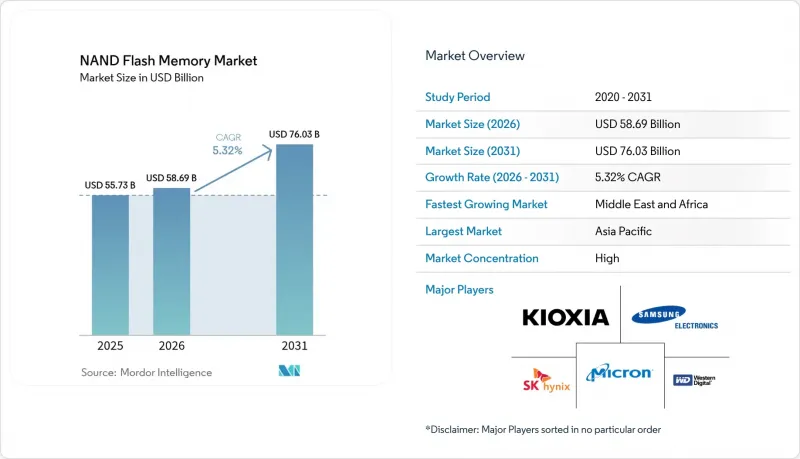
Mordor Intelligence에 의하면, 2026년 낸드플래시 메모리 시장 규모는 586억 9,000만 달러로 추정되고 2025년 557억 3,000만 달러에서 확대해, 2031년에는 760억 3,000만 달러에 이를 것으로 예측됩니다.
2026-2031년 동안 연평균 성장률(CAGR) 5.32%로 성장할 것으로 전망됩니다.

본 보고서는 유형(SLC(싱글 레벨 셀), MLC(멀티 레벨 셀), TLC(트리플 레벨 셀), QLC(쿼드 레벨 셀)), 구조(2D(평면형) NAND, 3D NAND),인터페이스(SATA, PCIe/NVMe, UFS/eMMC), 용도(스마트폰, SSD(PC·게임기), 엔터프라이즈/데이터센터용 SSD, 기타), 지역별로 분류되어 있습니다. 시장 예측은 금액(달러) 기준으로 제시되어 있습니다.
세계의 낸드플래시 메모리 시장 동향 및 인사이트
데이터센터 내 AI/ML 스토리지의 급증
하이퍼스케일 사업자들은 NVMe SSD 풀을 GPU 클러스터 근처에 배치할 수 있도록 스토리지 계층을 재설계하고 있으며, 검색 및 확장형 생성 워크로드에 대해 초당 수 기가바이트의 처리량을 유지하고 있습니다. 웨스턴디지털은 5G 지원 엔드포인트만으로도 2029년까지 NAND의 누적 수요가 1만 9,000 페타바이트에 달할 것으로 추정하며, 메모리와 콜드 스토리지 간의 성능 격차를 해소하는 데 플래시가 수행하는 역할의 중요성을 부각시키고 있습니다. 조달 로드맵에서는 30TB에서 100TB 용량의 엔터프라이즈용 드라이브가 점점 더 중요해지고 있으며, 이러한 변화는 2024년에 발표된 삼성의 128TB BM1743 SSD에서도 드러납니다. 그로 인한 파급 효과로 인해 낸드플래시 메모리 시장의 성장세를 유지하기 위한 레이어 수 혁신과 컨트롤러 수준의 압축 기술이 가속화되고 있습니다.
5G 및 대규모 IoT 기기의 보급
독립형 5G 도입으로 인해 엣지 분석 이용 사례, 스마트 팩토리, 커넥티드카, 스마트 그리드가 가능해졌으며, 이러한 기술들은 실시간 의사 결정 엔진을 위해 로컬 비휘발성 스토리지를 필수로 합니다. 웨스턴 디지털의 백서에 따르면, 용량이 8GB를 초과하면 산업용 모듈에서 NOR에서 NAND로의 전환이 일어날 것으로 예측됩니다. 현재 반도체 로드맵에서는 광범위한 온도 범위를 지원하는 QLC 다이와 자동차용 인증을 받은 NVMe 설계가 우선시되고 있으며, 이로 인해 낸드플래시 메모리 시장의 영역이 운송 및 인프라 부문으로 확대되고 있습니다.
고밀도 셀의 수명 한계
QLC의 1,000-3,000회 쓰기/지우기 사이클이라는 임계값은 로그 양이 많은 데이터베이스에는 여전히 불충분하여, 비용 이점을 저해하는 오버프로비저닝을 불가피하게 만들고 있습니다. Hackaday는 300층 스택에서 전자 트랩의 마모가 가속화됨에 따라 물리적 한계에 가까워지고 있다고 지적합니다. 고급 오류 정정 및 마모 균등화 알고리즘을 통해 성능 저하는 상쇄되지만, PLC나 크로스포인트와 같은 대체 메모리가 여전히 주목받고 있으며, 내구성이 입증될 때까지는 낸드플래시 메모리 시장의 일부 성장을 억제할 것으로 보입니다.
부문별 분석
TLC 디바이스의 낸드플래시 메모리 시장 규모는 내구성과 비용의 균형이 뛰어나기 때문에 63.58%의 시장 점유율을 차지하고 있습니다. 한편, QLC는 하이퍼스케일러 각사가 AI 데이터 레이크에서 8-16배의 밀도 우위를 입증함에 따라 연평균 성장률(CAGR) 6.35%로 급속히 성장하고 있으며, 이에 따라 2031년까지 QLC가 차지하는 낸드플래시 메모리 시장 전체 점유율은 확대될 전망입니다. Samsung Electronics가 개발한 280층 QLC 프로토타입은 16TB 단면 M.2 드라이브에 적용된 로드맵을 보여주고 있으며, 추론 클러스터의 처리량 요구 사항을 충족하면서도 랙의 설치 면적을 축소합니다. 컨트롤러 수준의 SLC 캐시 기술과 온다이 ECC 덕분에 TLC와의 지연 시간 차이가 줄어들고 있어, VOD 라이브러리나 백업 리포지토리 등 광범위한 워크로드의 전환이 촉진되고 있습니다. TLC는 1만 사이클 이상의 내구 수명으로 예측 가능한 서비스 품질이 보장되는 쓰기 집약적인 ERP 및 OLTP 환경에서 계속해서 우위를 유지할 것으로 보입니다.
소비자용 노트북에서는 TLC의 뛰어난 전력 소비 특성으로 인해 도입 기반이 유지되고 있지만, QLC의 비트당 단가 하락으로 인해 이미 미드레인지 SKU에는 압박이 가해지고 있습니다. 마이크론의 6세대 QLC는 1세대 샘플에 비해 읽기 지연 시간이 34% 감소하여, 기존에 인식되던 성능 격차를 좁히고 있습니다. 펌웨어를 통한 수명 연장 대책이 성숙해짐에 따라, 각 OEM 업체들은 대용량 SKU에는 QLC를 채택하고, 프리미엄 라인에는 계속해서 고성능 TLC 노드를 채택하는 계층화된 제품 라인업을 도입할 가능성이 높습니다. 이러한 상호작용으로 인해, 예측 기간 동안 두 기술은 낸드플래시 메모리 시장의 중심적인 위치를 계속 유지할 것으로 보입니다.
평면 구조에서 수직 적층으로의 전환은 사실상 완료되었으며, 2025년에는 3D NAND가 낸드플래시 메모리 시장 점유율의 86.85%를 차지했습니다. 적층 수의 비약적인 발전, 즉 SK하이닉스의 상용 321층 TLC와 삼성의 400층 이상 V-NAND는 이번 10년이 끝나기 전에 500층이라는 고비를 넘어 자신 있게 스케일링이 진행될 것임을 시사합니다. 그 경제적 타당성은 명백합니다. 수직 스케일링은 셀 크기를 축소하지 않고도 용량을 증가시켜 리소그래피의 제약을 회피합니다. 2D NAND는 용량보다는 초저지연 쓰기 성능이 중시되는 항공우주 및 방위 분야의 틈새 모듈에서 여전히 사용되고 있습니다.
층 수가 증가하면 상호 연결 저항과 셀 간 간섭에 부담이 가해집니다. 이를 극복하기 위해 키오크시아의 CMOS 본딩 어레이 전략은 주변 회로를 분리함으로써 I/O 효율을 높이고, 초고층 스택에서의 수율을 향상시키고 있습니다. Samsung Electronics가 크리미 인터페이스 게이트용 하프늄 강유전체를 연구하고 있는 것도, 스택 높이가 증가하더라도 임계 전압의 여유를 유지하는 것을 목표로 하는 것과 같은 목적에서입니다.
지역별 분석
2025년에는 아시아태평양이 매출의 55.40%를 차지했으며, 그 중심에는 한국의 수직 통합형 대기업과 중국의 거대한 디바이스 조립 거점이 있었습니다. 삼성의 9세대 V-NAND(286층) 양산과 SK 하이닉스의 321층 TLC 라인은 이 지역의 기술적 우위를 입증하고 있습니다. 베이징의 국내 대기업인 YMTC는 수출 규제 제약에도 불구하고 232층 QLC 노드 개발을 추진하고 있으며, 낸드플래시 메모리 시장에서 아시아태평양의 압도적인 영향력을 유지하기 위한 자국 주도적인 생산 능력 확대를 보여주고 있습니다.
북미는 클라우드 부문의 활발한 설비 투자에 힘입어 매출 순위에서 2위를 차지하고 있습니다. ‘CHIPS and Science Act’는 마이크론(Micron)사의 1,250억 달러 규모 미국 내 메가팹 건설 계획에 자금을 지원하여, 2035년까지 미국의 첨단 메모리 자급률 향상을 도모하고 있습니다. 캐나다는 컨트롤러 IP 설계 인력을 공급하고, 멕시코는 USMCA(미국·멕시코·캐나다 협정) 규정에 따라 모듈 수준의 조립 라인을 확대하고 있으며, 이들이 힘을 합쳐 지역공급 다각화를 강화하고 있습니다.
유럽은 메모리 웨이퍼 제조 능력의 한계로 인해 시장 점유율이 한 자릿수 중반에 머물러 있습니다. 독일과 프랑스의 자동차 및 산업용 OEM 기업들로부터 자동차용 NVMe 모듈에 대한 견조한 수요가 발생하고 있습니다. ‘유럽 그린 딜’ 등 지속가능성에 관한 지침에 따라, 구매자들의 관심은 랙의 에너지 밀도를 낮추는 저전력형 PCIe 5.0 SSD로 쏠리고 있습니다. 유럽의 팹(fab) 기업들은 읽기 시 에너지 소비량이 3 pJ/비트 이하인 차세대 3D NAND 노드를 통해 이 틈새 시장에서 점유율을 확보하는 것을 목표로 하고 있습니다.
중동 및 아프리카는 연평균 성장률(CAGR) 8.21%로 가장 높은 성장률을 보이고 있습니다. 사우디아라비아의 ‘비전 2030’은 리야드 주변에 웨이퍼부터 백엔드에 이르는 복합 시설 건설을 뒷받침하고 있는 반면, 아부다비의 정부계 투자자들은 지역 공급망 구축을 촉진하기 위해 컨트롤러 전문 기업과의 합작 투자를 모색하고 있습니다. 풍부한 재생에너지 개발 프로젝트와 매력적인 세제가 패키징 파트너들을 끌어들이고 있으며, GCC(걸프협력회의) 회원국 전역의 데이터 허브에서 낸드플래시 메모리 시장의 확산을 뒷받침할 현지 생산 기반이 마련되고 있습니다.
기타 혜택
- 엑셀 형식 시장 예측(ME) 시트
- 3개월간의 애널리스트 지원
자주 묻는 질문
목차
제1장 서론
제2장 조사 방법
제3장 주요 요약
제4장 시장 구도
제5장 시장 규모 및 성장 예측
제6장 경쟁 구도
제7장 시장 기회 및 향후 전망
KTH 26.09.08According to Mordor Intelligence, NAND flash memory market size in 2026 is estimated at USD 58.69 billion, growing from 2025 value of USD 55.73 billion with 2031 projections showing USD 76.03 billion, growing at 5.32% CAGR over 2026-2031.
This report is Segmented by Type (SLC (Single-Level Cell), MLC (Multi-Level Cell), TLC (Triple-Level Cell), and QLC (Quad-Level Cell)), Structure (2D (Planar) NAND, and 3D NAND), Interface (SATA, Pcie / NVMe, and UFS / EMMC), Application (Smartphones, Solid-State Drives (PC and Console), Enterprise / Data-Center SSD, and More), and Geography. The Market Forecasts are Provided in Terms of Value (USD).
Global NAND Flash Memory Market Trends and Insights
Data-center AI/ML storage surge
Hyperscale operators are redesigning storage hierarchies so that NVMe SSD pools sit closer to GPU clusters, sustaining multi-gigabyte-per-second throughput for retrieval-augmented generation workloads. Western Digital estimates cumulative demand of 19,000 petabytes of NAND by 2029 for 5G-enabled endpoints alone, underscoring flash's role in bridging memory and cold-storage performance gaps. Procurement roadmaps increasingly favor 30 TB to 100 TB enterprise drives, a shift visible in Samsung's 128 TB BM1743 SSD showcased in 2024. The resulting pull-through effect accelerates layer-count innovation and controller-level compression techniques that sustain the NAND flash memory market momentum.
5G and massive-IoT device proliferation
Standalone 5G deployments unlock edge analytics use cases, smart factories, connected cars, and smart grids that mandate local non-volatile storage for real-time decision engines. Western Digital's white paper anticipates a NOR-to-NAND crossover within industrial modules as capacities climb above 8 GB. Semiconductor roadmaps now prioritize extended-temperature QLC die and automotive-qualified NVMe designs, broadening the NAND flash memory market footprint across transportation and infrastructure domains.
Endurance limits of high-density cells
QLC's 1,000-3,000 program/erase thresholds remain insufficient for log-heavy databases, forcing over-provisioning that erodes cost benefits. Hackaday notes the physics ceiling approaching as electron-trap wear accelerates in 300-layer stacks. Although advanced error-correction and wear-leveling algorithms offset degradation, alternate memories such as PLC or cross-point remain on the horizon, tempering portions of the NAND flash memory market until longevity is proven.
Other drivers and restraints analyzed in the detailed report include:
- PC/Console transition from HDD to SSD
- Enterprise pivot to cost-efficient QLC SSDs
- Pricing cyclicality and cap-ex burden
For complete list of drivers and restraints, kindly check the Table Of Contents.
Segment Analysis
The NAND flash memory market size for TLC devices held a 63.58% market share with the strength of balanced endurance and cost. QLC, however, is accelerating at 6.35% CAGR as hyperscalers validate its 8-16X density advantage for AI data-lakes, which lifts the overall NAND flash memory market share allocated to QLC by 2031. Samsung's 280-layer QLC prototype signals a roadmap to 16 TB single-sided M.2 drives, shrinking rack footprints while meeting throughput rules for inference clusters. Controller-level SLC-cache techniques and on-die ECC are narrowing the latency gap with TLC, encouraging broader workloads such as VOD libraries and backup repositories to migrate. TLC will retain primacy in write-intensive ERP and OLTP environments where its 10,000-plus cycle rating secures predictable quality-of-service.
In consumer notebooks, TLC's favorable power profile sustains its install base, but falling QLC cost-per-bit is already pressuring mid-range SKUs. Micron's sixth-gen QLC exhibits 34% lower read latency than first-gen samples, eroding the perceived performance divide. As firmware-defined endurance mitigation matures, OEMs will likely introduce tiered offerings where high-capacity SKUs employ QLC, while premium lines continue on advanced TLC nodes. This interplay keeps both technologies central to the NAND flash memory market over the forecast horizon.
The shift from planar to vertical stacking is virtually complete: 3D NAND commanded 86.85% of the NAND flash memory market share in 2025. Layer-count breakthroughs, SK Hynix's commercial 321-layer TLC and Samsung's 400-plus-layer V-NAND, signal confident scaling beyond the 500-layer watermark before decade-end. The economic logic is clear; vertical scaling adds capacity without shrinking cell size, sidestepping lithography constraints. 2D NAND survives in niche aerospace and defense modules where ultra-low-latency writes outweigh capacity.
Layer additions do stress interconnect resistance and cell-to-cell interference. To overcome this, Kioxia's CMOS-bonded-array strategy decouples peripheral circuits, boosting I/O efficiency and improving yield in ultra-tall stacks. Samsung's exploration of hafnia ferroelectrics for creamy-interface gates pursues a similar aim: maintain threshold-voltage margins even as stack height extends.
Complete Report Scope:
- By Type
- SLC (Single-Level Cell)
- MLC (Multi-Level Cell)
- TLC (Triple-Level Cell)
- QLC (Quad-Level Cell)
- By Structure
- 2D (Planar) NAND
- 3D NAND
- By Interface
- SATA
- PCIe / NVMe
- UFS / eMMC
- By Application
- Smartphones
- Solid-State Drives (PC and Console)
- Enterprise / Data-center SSD
- Memory Cards and USB Drives
- Industrial and Automotive Electronics
- By Geography
- North America
- United States
- Canada
- Mexico
- South America
- Brazil
- Argentina
- Rest of South America
- Europe
- Germany
- United Kingdom
- France
- Italy
- Spain
- Russia
- Rest of Europe
- Asia-Pacific
- China
- Japan
- India
- South Korea
- South-East Asia
- Rest of Asia-Pacific
- Middle East and Africa
- Middle East
- Saudi Arabia
- United Arab Emirates
- Turkey
- Rest of Middle East
- Africa
- South Africa
- Nigeria
- Rest of Africa
- Middle East
- North America
Geography Analysis
Asia-Pacific contributed 55.40% of sales in 2025, anchored by South Korea's vertically-integrated champions and China's colossal device assembly base. Samsung's mass production of 9th-generation V-NAND (286 layers) and SK Hynix's 321-layer TLC line affirm the region's technology lead. Beijing's domestic champion YMTC pushes 232-layer QLC nodes despite export-control constraints, illustrating indigenous capacity expansion that preserves Asia-Pacific's outsized influence on the NAND flash memory market.
North America sits second on revenue league tables, propelled by cloud capital-expenditure intensity. The CHIPS and Science Act bankrolls Micron's USD 125 billion state-side megafab roadmap, lifting U.S. advanced-memory self-sufficiency by 2035. Canada contributes controller-IP design talent, while Mexico scales module-level assembly lines under USMCA provisions, together reinforcing regional supply diversification.
Europe registers mid-single-digit share, constrained by limited memory wafer fabrication. Nonetheless, automotive and industrial OEMs in Germany and France generate robust demand for auto-grade NVMe modules. Sustainability directives such as the European Green Deal pivot buyers toward power-efficient PCIe 5.0 SSDs that lower rack energy density, a niche European fabs aim to capture through next-generation 3D NAND nodes with under-3 pJ/bit read energy footprints.
The Middle East and Africa present the highest growth rate at 8.21% CAGR. Saudi Arabia's Vision 2030 underwrites wafer-to-back-end complexes around Riyadh, while Abu Dhabi's sovereign investors explore joint-ventures with controller specialists to bootstrap a regional supply chain. Ample renewable-energy pipelines and attractive tax regimes draw packaging partners, setting the stage for localized production that boosts the NAND flash memory market penetration across GCC data hubs.
- Samsung Electronics Co., Ltd.
- SK hynix Inc.
- KIOXIA Holdings Corporation
- Western Digital Corporation
- Micron Technology, Inc.
- Nanya Technology Corporation
- Powerchip Technology Corporation
- Winbond Electronics Corporation
- Macronix International Co., Ltd.
- Silicon Motion Technology Corp.
- Phison Electronics Corp.
- Kingston Technology Company, Inc.
- ADATA Technology Co., Ltd.
- Transcend Information, Inc.
- GigaDevice Semiconductor Inc.
- SK Group (Solid-State Storage division)
- PNY Technologies, Inc.
- Team Group Inc.
- Longsys Electronics Co., Ltd.
- Smart Modular Technologies, Inc.
Additional Benefits:
- The market estimate (ME) sheet in Excel format
- 3 months of analyst support
TABLE OF CONTENTS
1 INTRODUCTION
- 1.1 Study Assumptions and Market Definition
- 1.2 Scope of the Study
2 RESEARCH METHODOLOGY
3 EXECUTIVE SUMMARY
4 MARKET LANDSCAPE
- 4.1 Market Overview
- 4.2 Market Drivers
- 4.2.1 Data-center AI/ML storage surge
- 4.2.2 5G and massive-IoT device proliferation
- 4.2.3 PC/Console transition from HDD to SSD
- 4.2.4 Enterprise pivot to cost-efficient QLC SSDs
- 4.2.5 National on-shore NAND fab programs
- 4.2.6 CXL-enabled computational storage adoption
- 4.3 Market Restraints
- 4.3.1 Endurance limits of high-density cells
- 4.3.2 Pricing cyclicality and cap-ex burden
- 4.3.3 Export-control induced equipment bottlenecks
- 4.3.4 Sustainability scrutiny on high-layer fabs
- 4.4 Industry Supply Chain Analysis
- 4.5 Regulatory Landscape
- 4.6 Technological Outlook
- 4.7 Impact of Macroeconomic Factors
- 4.8 Porter's Five Forces Analysis
- 4.8.1 Bargaining Power of Suppliers
- 4.8.2 Bargaining Power of Buyers
- 4.8.3 Threat of New Entrants
- 4.8.4 Threat of Substitutes
- 4.8.5 Intensity of Competitive Rivalry
5 MARKET SIZE AND GROWTH FORECASTS (VALUE)
- 5.1 By Type
- 5.1.1 SLC (Single-Level Cell)
- 5.1.2 MLC (Multi-Level Cell)
- 5.1.3 TLC (Triple-Level Cell)
- 5.1.4 QLC (Quad-Level Cell)
- 5.2 By Structure
- 5.2.1 2D (Planar) NAND
- 5.2.2 3D NAND
- 5.3 By Interface
- 5.3.1 SATA
- 5.3.2 PCIe / NVMe
- 5.3.3 UFS / eMMC
- 5.4 By Application
- 5.4.1 Smartphones
- 5.4.2 Solid-State Drives (PC and Console)
- 5.4.3 Enterprise / Data-center SSD
- 5.4.4 Memory Cards and USB Drives
- 5.4.5 Industrial and Automotive Electronics
- 5.5 By Geography
- 5.5.1 North America
- 5.5.1.1 United States
- 5.5.1.2 Canada
- 5.5.1.3 Mexico
- 5.5.2 South America
- 5.5.2.1 Brazil
- 5.5.2.2 Argentina
- 5.5.2.3 Rest of South America
- 5.5.3 Europe
- 5.5.3.1 Germany
- 5.5.3.2 United Kingdom
- 5.5.3.3 France
- 5.5.3.4 Italy
- 5.5.3.5 Spain
- 5.5.3.6 Russia
- 5.5.3.7 Rest of Europe
- 5.5.4 Asia-Pacific
- 5.5.4.1 China
- 5.5.4.2 Japan
- 5.5.4.3 India
- 5.5.4.4 South Korea
- 5.5.4.5 South-East Asia
- 5.5.4.6 Rest of Asia-Pacific
- 5.5.5 Middle East and Africa
- 5.5.5.1 Middle East
- 5.5.5.1.1 Saudi Arabia
- 5.5.5.1.2 United Arab Emirates
- 5.5.5.1.3 Turkey
- 5.5.5.1.4 Rest of Middle East
- 5.5.5.2 Africa
- 5.5.5.2.1 South Africa
- 5.5.5.2.2 Nigeria
- 5.5.5.2.3 Rest of Africa
- 5.5.5.1 Middle East
- 5.5.1 North America
6 COMPETITIVE LANDSCAPE
- 6.1 Market Concentration
- 6.2 Strategic Moves
- 6.3 Market Share Analysis
- 6.4 Company Profiles (includes Global level Overview, Market level overview, Core Segments, Financials as available, Strategic Information, Market Rank/Share for key companies, Products and Services, and Recent Developments)
- 6.4.1 Samsung Electronics Co., Ltd.
- 6.4.2 SK hynix Inc.
- 6.4.3 KIOXIA Holdings Corporation
- 6.4.4 Western Digital Corporation
- 6.4.5 Micron Technology, Inc.
- 6.4.6 Nanya Technology Corporation
- 6.4.7 Powerchip Technology Corporation
- 6.4.8 Winbond Electronics Corporation
- 6.4.9 Macronix International Co., Ltd.
- 6.4.10 Silicon Motion Technology Corp.
- 6.4.11 Phison Electronics Corp.
- 6.4.12 Kingston Technology Company, Inc.
- 6.4.13 ADATA Technology Co., Ltd.
- 6.4.14 Transcend Information, Inc.
- 6.4.15 GigaDevice Semiconductor Inc.
- 6.4.16 SK Group (Solid-State Storage division)
- 6.4.17 PNY Technologies, Inc.
- 6.4.18 Team Group Inc.
- 6.4.19 Longsys Electronics Co., Ltd.
- 6.4.20 Smart Modular Technologies, Inc.
7 MARKET OPPORTUNITIES AND FUTURE OUTLOOK
- 7.1 White-space and Unmet-Need Assessment