

|
시장보고서
상품코드
2123025
갈륨비소(GaAs) 웨이퍼 시장 : 점유율 분석, 업계 동향과 통계, 성장 예측(2026-2031년)Gallium Arsenide GaAs Wafer - Market Share Analysis, Industry Trends & Statistics, Growth Forecasts (2026 - 2031) |
||||||
 Mordor Intelligence
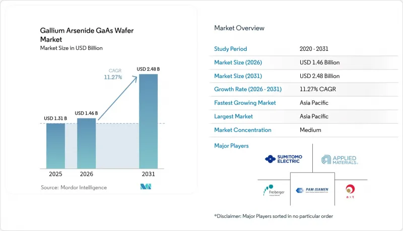
Mordor Intelligence에 의하면, 2026년 갈륨비소(GaAs) 웨이퍼 시장 규모는 14억 6,000만 달러로 추정되고 있어 2025년 13억 1,000만 달러에서 확대해, 2031년에는 24억 8,000만 달러에 이를 것으로 예측됩니다.
2026-2031년 동안 연평균 성장률(CAGR) 11.27%로 성장할 것으로 전망됩니다.
본 보고서는 용도별(무선 주파수(RF) 전자기기, 기타), 웨이퍼 직경별(2인치, 3인치, 4인치, 기타),성장 기술별(LEC, VGF, 기타), 최종 이용 산업별(통신·5G 인프라, 기타), 전도성 유형별(반절연성 GaAs, 반전도성 GaAs), 지역별(북미, 기타)로 분류되어 있습니다. 시장 예측은 금액(달러) 단위로 제시되어 있습니다.
전 세계 갈륨비소(GaAs) 웨이퍼 시장 동향 및 인사이트
5G 인프라 구축이 GaAs RF 수요를 견인
통신 사업자들은 고밀도 5G 매크로셀 및 스몰셀 기지국을 구축하고 있으며, 여기에는 28GHz를 훨씬 초과하는 주파수 대역에서 선형 출력을 유지할 수 있는 전력 증폭기가 필요하지만, 실리콘 LDMOS는 이 영역에서 성능이 저하됩니다. 갈륨비소 웨이퍼는 약 8,500cm2/V*s의 전자 이동도를 실현하여, 도시 지역의 커버리지를 확보하기 위한 매시브 MIMO 어레이에서 신호의 무결성을 유지하는 고효율 프런트엔드 모듈을 가능하게 합니다. 각 네트워크 벤더는 수직 통합형 GaAs 제조업체와 수년에 걸친 공급 계약을 체결하고 있으며, 이를 통해 4G 하드웨어의 업데이트 주기가 2027년까지 예측 가능한 수요로 전환되었습니다.
광전자 소자의 붐(VCSEL, 레이저)
하이퍼스케일 데이터센터는 저지연 및 저전력 소모를 실현하기 위해 GaAs 기반 VCSEL 어레이를 채택한 400G 및 800G 광통신 디바이스로 전환하고 있습니다. 스마트폰 제조업체들은 생체 인증 모듈에 3D 센싱용 VCSEL을 탑재하고 있으며, 자동차 OEM 각사는 LiDAR용으로 GaAs 레이저를 채택하고 있습니다. 에피택셜 재성장 기술의 발전으로 방열성이 향상되고, 소자의 수명이 연장되어 웨이퍼의 평균 판매 가격(ASP)이 높은 수준을 유지하고 있습니다.
Si·SiC에 비해 높은 제조 비용
GaAs 결정의 추출에는 가압된 비소 가스 환경과 유독 가스 취급이 필요하며, 이로 인해 설비 투자(CapEx)와 운영 비용(Opex)이 실리콘보다 높아집니다. 4인치나 6인치와 같은 소형 형태에서는 300mm 실리콘의 ‘웨이퍼당 다이 수’가 제공하는 경제성에 미치지 못하여, 가격에 민감한 소비자용 가제트에서 GaAs의 채택을 제한하고 있습니다.
부문 분석
2025년에는 파워 앰프와 스위치가 5G 인프라 업그레이드의 핵심을 여전히 차지하고 있기 때문에 무선 주파수(RF) 전자 제품이 매출의 43.65%를 차지했습니다. 갈륨비소(GaAs) 웨이퍼 시장 규모에서 이 비율은 스몰 셀의 고밀도화 계획에 따라 꾸준히 상승할 것으로 예측됩니다. VCSEL 상호 연결 및 AR/VR용 광학 소자에 힘입어 포토닉스 및 이미징 디바이스는 연평균 성장률(CAGR) 13.25%로 다른 모든 용도를 능가하는 성장을 보일 것으로 예상되며, 이에 따라 갈륨비소(GaAs) 웨이퍼 시장의 향후 출하량은 재편될 전망입니다.
스마트폰 제조업체들이 VCSEL 기반 얼굴 인식 모듈을 통합함에 따라, 부문 간 수요 파급 효과가 발생하고 있으며, 이는 공통된 6인치 에피택셜 라인에서 포토닉스와 RF의 생산량 모두를 끌어올리고 있습니다. GaAs를 사용한 태양전지는 여전히 우주선용 틈새 시장에 머물러 있지만, 새로운 헤테로 통합 개념을 통해 다중 접합 설계가 지상의 집광형 어레이에 도입될 가능성이 있습니다.
4인치 기판은 성숙한 제조 설비 덕분에 여전히 매출의 35.85%를 차지하고 있지만, 생산 능력 관련 발표에 따르면 6인치 라인이 연평균 성장률(CAGR) 12.85%로 증가분 수요 대부분을 흡수하게 될 것입니다. 이러한 전환으로 인해 1회 제조당 다이 수가 증가하고 고정비가 분산됨에 따라, 갈륨비소(GaAs) 웨이퍼 시장 전체의 평균 판매 가격(ASP)은 하락하는 추세를 보이고 있습니다.
각 장비 공급업체들은 6인치를 초과하는 규모로 확장하기 위해 온도 구배 제어 및 비소 증기 관리에 주력하고 있습니다. 초기 8인치 시범 생산은 유망한 결과를 보여주고 있지만, 상용화에는 결함률을 더욱 낮춰야 합니다.
지역별 분석
아시아태평양은 에피택셜 제조 라인의 집적, 탄탄한 하청 기반, 정부 주도의 5G 인프라 구축에 힘입어 2025년에는 갈륨비소(GaAs) 웨이퍼 시장의 60.10%를 차지했습니다. 정부의 우대 조치로 인해 중국 본토에서는 화합물 반도체 팹의 확장이 진행되고 있는 반면, 대만과 한국은 파운드리 및 장비 부문에서의 시너지 효과를 통해 공급의 다양성을 강화하고 있습니다.
북미는 안전한 국내 생산이 필요한 항공우주 및 방위 부문 수요에 힘입어 2위를 차지하고 있습니다. 최근 ‘CHIPS법’에 따른 인센티브로 레이더 및 위성 프로그램용 반절연 소재 전용의 새로운 결정 성장로와 클린룸에 자금이 공급되면서, 장기적인 국내 공급 체제가 확고해지고 있습니다.
유럽은 자동차 및 산업용 자동화 부문에서 여전히 강점을 보이고 있습니다. Tier 1 공급업체들은 ADAS 레이더 및 공장용 센싱을 지원하기 위해 GaAs 파워 디바이스를 조달하고 있는 반면, 엄격한 환경 지침은 웨이퍼 재생과 관련된 순환 경제에 대한 조사를 촉진하고 있습니다. EU의 협력적 자금 지원을 통해 150mm 화합물 반도체 웨이퍼 파일럿 라인이 지원되고 있으며, 아시아와의 생산 능력 격차를 줄이는 것을 목표로 하고 있습니다.
기타 혜택
- 엑셀 형식 시장 예측(ME) 시트
- 3개월간의 애널리스트 지원
자주 묻는 질문
목차
제1장 서론
제2장 조사 방법
제3장 주요 요약
제4장 시장 구도
제5장 시장 규모와 성장 예측
제6장 경쟁 구도
제7장 시장 기회와 향후 전망
JHS 26.09.09According to Mordor Intelligence, gallium arsenide wafer market size in 2026 is estimated at USD 1.46 billion, growing from 2025 value of USD 1.31 billion with 2031 projections showing USD 2.48 billion, growing at 11.27% CAGR over 2026-2031.
This report is Segmented by Application (Radio-Frequency Electronics, and More), Wafer Diameter (2 Inch, 3 Inch, 4 Inch, and More), Growth Technology (LEC, VGF, and More), End-Use Industry (Telecom and 5G Infrastructure, and More), Conductivity Type (Semi-Insulating GaAs, Semi-Conducting GaAs), and Geography (North America, and More). The Market Forecasts are Provided in Terms of Value (USD).
Global Gallium Arsenide GaAs Wafer Market Trends and Insights
5G Infrastructure Roll-out Fuels GaAs RF Demand
Telecom operators are deploying dense 5G macro- and small-cell sites that require power amplifiers sustaining linear output well above 28 GHz, where silicon LDMOS falters. Gallium arsenide wafers deliver electron mobility around 8,500 cm2/V*s, enabling efficient front-end modules that preserve signal integrity in massive-MIMO arrays for urban coverage. Network vendors lock multiyear supply contracts with vertically integrated GaAs houses, converting 4G hardware refresh cycles into predictable demand through 2027.
Optoelectronic Device Boom (VCSELs, Lasers)
Hyperscale data centers move to 400G and 800G optics that rely on GaAs-based VCSEL arrays for lower latency and power draw. Smartphone makers embed 3D-sensing VCSELs in biometric modules, while automotive OEMs adopt GaAs lasers for LiDAR. Epitaxial regrowth advances improve thermal dissipation, extending device lifetimes and sustaining premium wafer ASPs.
High Production Cost vs Si and SiC
GaAs crystal pulling needs pressurized arsenic atmospheres and toxic-gas handling that raise CapEx and Opex above silicon. Smaller 4-inch and 6-inch formats cannot match the die-per-wafer economics of 300 mm silicon, limiting GaAs uptake in price-sensitive consumer gadgets.
Other drivers and restraints analyzed in the detailed report include:
- Aerospace and Defense Uptake for High-Frequency Radar
- Asian Epitaxy Capacity Boosts Supply and Lowers ASP
- Gallium Supply Concentration and Export Controls
For complete list of drivers and restraints, kindly check the Table Of Contents.
Segment Analysis
RF electronics held 43.65% revenue in 2025 as power amplifiers and switches remain core to 5G infrastructure upgrades. This portion of the Gallium arsenide wafer market size is forecast to climb steadily alongside small-cell densification plans. Photonic and imaging devices, propelled by VCSEL interconnects and AR/VR optics, are set to outpace all other uses at 13.25% CAGR, thereby reshaping future volumes of the Gallium arsenide wafer market.
Cross-segment pull-through emerges as handset makers integrate VCSEL-based face ID modules, boosting both photonics and RF volume on common 6-inch epi lines. Solar cells on GaAs remain a niche for spacecraft, yet new heterointegration concepts could push multi-junction designs into terrestrial concentrator arrays.
Four-inch substrates still command 35.85% revenue thanks to mature tooling, but capacity announcements reveal that 6-inch lines will absorb most incremental demand at 12.85% CAGR. The shift improves die counts per run and spreads fixed costs, nudging the overall Gallium arsenide wafer market toward lower ASPs.
Equipment vendors tackle thermal-gradient control and arsenic vapor management to scale beyond 6 inches. Early 8-inch pilot runs show promise yet require further defect reduction before commercial deployment.
Complete Report Scope:
- By Application
- Radio-Frequency Electronics
- Optical and IR LEDs
- Photovoltaic / Solar Cells
- Photonic and Imaging Devices
- Other Applications
- By Wafer Diameter
- 2 inch (50 mm)
- 3 inch (76 mm)
- 4 inch (100 mm)
- 6 inch (150 mm)
- 8 inch (200 mm) and Above
- By Growth Technology
- Liquid-Encapsulated Czochralski (LEC)
- Vertical Gradient Freeze (VGF)
- Horizontal Bridgman (HB)
- Molecular Beam Epitaxy (MBE)
- Metal-Organic CVD (MOCVD)
- By End-Use Industry
- Telecom and 5G Infrastructure
- Consumer Electronics
- Aerospace and Defense
- Automotive (ADAS, EV)
- Industrial and Energy
- By Conductivity Type
- Semi-insulating GaAs
- Semi-conducting GaAs (n-/p-type)
- By Geography
- North America
- United States
- Canada
- Mexico
- South America
- Brazil
- Argentina
- Rest of South America
- Europe
- Germany
- United Kingdom
- France
- Italy
- Rest of Europe
- Asia-Pacific
- China
- Japan
- South Korea
- India
- Rest of Asia-Pacific
- Middle East
- Saudi Arabia
- United Arab Emirates
- Rest of Middle East
- Africa
- South Africa
- Rest of Africa
- North America
Geography Analysis
Asia-Pacific held 60.10% of the Gallium arsenide wafer market in 2025 thanks to clustered epitaxial lines, a deep subcontract base, and state-backed 5G build-outs. Government incentives help mainland China expand compound-semiconductor fabs, while Taiwan and South Korea provide foundry and equipment synergies that reinforce supply diversity.
North America ranks second, anchored by aerospace and defense demand requiring secure on-shore production. Recent CHIPS Act incentives finance new crystal-growth reactors and cleanrooms dedicated to semi-insulating material for radar and satellite programs, cementing long-term domestic supply.
Europe retains strength in automotive and industrial automation. Tier-1 suppliers source GaAs power devices to support ADAS radar and factory sensing, while stringent environmental directives spur circular-economy research on wafer reclamation. Coordinated EU funding backs pilot lines for 150 mm compound-semiconductor substrates, seeking to narrow the capacity gap with Asia.
- AXT Inc.
- China Crystal Technologies Co. Ltd.
- Freiberger Compound Materials GmbH
- Semiconductor Wafer Inc.
- Sumitomo Electric Industries, Ltd.
- Xiamen Powerway Advanced Material Co., Ltd.
- Wafer Technology Ltd.
- Vital Materials Co., Ltd.
- DOWA Electronics Materials Co., Ltd.
- American Elements, Inc.
- IQE plc
- WIN Semiconductors Corp.
- Advanced Wireless Semiconductor Co.
- Visual Photonics Epitaxy Co., Ltd. (VPEC)
- IntelliEPI, Inc.
- Global Communication Semiconductors, LLC
- Roditi Ltd.
- Veeco Instruments Inc.
- Applied Materials, Inc.
- AIXTRON SE
Additional Benefits:
- The market estimate (ME) sheet in Excel format
- 3 months of analyst support
TABLE OF CONTENTS
1 INTRODUCTION
- 1.1 Study Assumptions and Market Definition
- 1.2 Scope of the Study
2 RESEARCH METHODOLOGY
3 EXECUTIVE SUMMARY
4 MARKET LANDSCAPE
- 4.1 Market Overview
- 4.2 Market Drivers
- 4.2.1 5G infrastructure roll-out fuels GaAs RF demand
- 4.2.2 Optoelectronic device boom (VCSELs, lasers)
- 4.2.3 Aerospace and defense uptake for high-freq radar
- 4.2.4 Asian epitaxy capacity boosts supply and lowers ASP
- 4.2.5 Micro-LED adoption in AR/VR wearables
- 4.2.6 Remote-epitaxy substrate reuse cuts wafer cost
- 4.3 Market Restraints
- 4.3.1 High production cost vs Si and SiC
- 4.3.2 Gallium supply concentration and export controls
- 4.3.3 GaN and SiC competition in RF / power
- 4.3.4 Environmental and safety compliance
- 4.4 Industry Value Chain Analysis
- 4.5 Regulatory Landscape
- 4.6 Technological Outlook
- 4.7 Porter's Five Forces Analysis
- 4.7.1 Bargaining Power of Suppliers
- 4.7.2 Bargaining Power of Buyers
- 4.7.3 Threat of New Entrants
- 4.7.4 Threat of Substitute Products
- 4.7.5 Intensity of Competitive Rivalry
5 MARKET SIZE AND GROWTH FORECASTS (VALUE)
- 5.1 By Application
- 5.1.1 Radio-Frequency Electronics
- 5.1.2 Optical and IR LEDs
- 5.1.3 Photovoltaic / Solar Cells
- 5.1.4 Photonic and Imaging Devices
- 5.1.5 Other Applications
- 5.2 By Wafer Diameter
- 5.2.1 2 inch (50 mm)
- 5.2.2 3 inch (76 mm)
- 5.2.3 4 inch (100 mm)
- 5.2.4 6 inch (150 mm)
- 5.2.5 8 inch (200 mm) and Above
- 5.3 By Growth Technology
- 5.3.1 Liquid-Encapsulated Czochralski (LEC)
- 5.3.2 Vertical Gradient Freeze (VGF)
- 5.3.3 Horizontal Bridgman (HB)
- 5.3.4 Molecular Beam Epitaxy (MBE)
- 5.3.5 Metal-Organic CVD (MOCVD)
- 5.4 By End-Use Industry
- 5.4.1 Telecom and 5G Infrastructure
- 5.4.2 Consumer Electronics
- 5.4.3 Aerospace and Defense
- 5.4.4 Automotive (ADAS, EV)
- 5.4.5 Industrial and Energy
- 5.5 By Conductivity Type
- 5.5.1 Semi-insulating GaAs
- 5.5.2 Semi-conducting GaAs (n-/p-type)
- 5.6 By Geography
- 5.6.1 North America
- 5.6.1.1 United States
- 5.6.1.2 Canada
- 5.6.1.3 Mexico
- 5.6.2 South America
- 5.6.2.1 Brazil
- 5.6.2.2 Argentina
- 5.6.2.3 Rest of South America
- 5.6.3 Europe
- 5.6.3.1 Germany
- 5.6.3.2 United Kingdom
- 5.6.3.3 France
- 5.6.3.4 Italy
- 5.6.3.5 Rest of Europe
- 5.6.4 Asia-Pacific
- 5.6.4.1 China
- 5.6.4.2 Japan
- 5.6.4.3 South Korea
- 5.6.4.4 India
- 5.6.4.5 Rest of Asia-Pacific
- 5.6.5 Middle East
- 5.6.5.1 Saudi Arabia
- 5.6.5.2 United Arab Emirates
- 5.6.5.3 Rest of Middle East
- 5.6.6 Africa
- 5.6.6.1 South Africa
- 5.6.6.2 Rest of Africa
- 5.6.1 North America
6 COMPETITIVE LANDSCAPE
- 6.1 Market Concentration
- 6.2 Strategic Moves
- 6.3 Market Share Analysis
- 6.4 Company Profiles (includes Global level Overview, Market level overview, Core Segments, Financials as available, Strategic Information, Market Rank/Share, Products and Services, Recent Developments)
- 6.4.1 AXT Inc.
- 6.4.2 China Crystal Technologies Co. Ltd.
- 6.4.3 Freiberger Compound Materials GmbH
- 6.4.4 Semiconductor Wafer Inc.
- 6.4.5 Sumitomo Electric Industries, Ltd.
- 6.4.6 Xiamen Powerway Advanced Material Co., Ltd.
- 6.4.7 Wafer Technology Ltd.
- 6.4.8 Vital Materials Co., Ltd.
- 6.4.9 DOWA Electronics Materials Co., Ltd.
- 6.4.10 American Elements, Inc.
- 6.4.11 IQE plc
- 6.4.12 WIN Semiconductors Corp.
- 6.4.13 Advanced Wireless Semiconductor Co.
- 6.4.14 Visual Photonics Epitaxy Co., Ltd. (VPEC)
- 6.4.15 IntelliEPI, Inc.
- 6.4.16 Global Communication Semiconductors, LLC
- 6.4.17 Roditi Ltd.
- 6.4.18 Veeco Instruments Inc.
- 6.4.19 Applied Materials, Inc.
- 6.4.20 AIXTRON SE
7 MARKET OPPORTUNITIES AND FUTURE OUTLOOK
- 7.1 White-space and Unmet-need Assessment


