

|
시장보고서
상품코드
2123026
인화인듐 웨이퍼 시장 : 점유율 분석, 업계 동향과 통계, 성장 예측(2026-2031년)Indium Phosphide Wafer - Market Share Analysis, Industry Trends & Statistics, Growth Forecasts (2026 - 2031) |
||||||
 Mordor Intelligence
Mordor Intelligence에 의하면, 인화인듐 웨이퍼 시장 규모는 2025년 1억 9,817만 달러에서 2026년에는 2억 2,142만 달러로 확대되어 2026-2031년까지 CAGR 11.73%로 성장을 지속하여, 2031년에는 3억 8,565만 달러에 이를 것으로 예측됩니다.
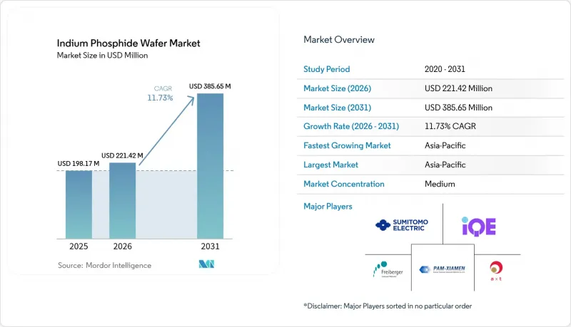
본 보고서는 직경(50.8mm, 76.2mm, 기타), 웨이퍼 도핑 유형별(비도핑 전도성, 기타),용도별(포토닉스·광트랜시버, 기타), 최종 사용자 산업별(전기통신·데이터 통신, 기타), 제조 기술별(VGF 공법으로 제조된 벌크 웨이퍼, 기타), 지역별(북미, 남미, 기타)로 분류되어 있습니다. 시장 예측은 금액(달러) 기준으로 제시되어 있습니다.
전 세계 인화인듐 웨이퍼 시장 동향 및 인사이트
고속 광트랜시버 수요 증가가 InP 채택을 가속화
800G 및 1.6T 링크로의 전환을 추진하는 클라우드 사업자들은 필요한 속도로 작동하는 에지 방출 레이저와 포토다이오드를 필요로 하지만, 이를 제공할 수 있는 것은 인화인듐(InP)뿐입니다. Coherent는 2024년 4분기에 InP 디바이스 생산량을 3배로 확대했으며, 현재 3.2T 트랜시버 샘플을 제공합니다. Source Photonics는 InP 기반 부품을 사용한 1.6T 코히런트 모듈을 시연함으로써, 코패키지드 옵틱스에서 이 소재가 필수적임을 입증했습니다. 스위치 ASIC이 51T 대역폭으로 진화함에 따라, 플러그형 광학 부품은 온보드 레이저 엔진으로 대체되고 있으며, 인화인듐 웨이퍼 시장에서 기판 수요가 감소하고 있습니다.
5G 인프라 구축이 mm파 수요를 견인
상용 5G 백홀은 28GHz 이상에서 작동하지만, 이 주파수 대역에서 InP HBT는 450GHz를 넘는 컷오프 주파수와 4.5V를 넘는 항복 전압을 실현합니다. 노키아가 인피네라를 23억 달러에 인수한 것은 전송 노드용 InP 코히런트 기술에 대한 전문 지식을 확보하기 위함입니다. 테라헤르츠 대역 주파수를 검토하고 있는 초기 6G 테스트베드에서는 610GHz까지 검증된 InP HEMT가 채택되고 있습니다. 그 결과, 인화인듐 웨이퍼 시장에서 광 프런트엔드뿐만 아니라 RF 체인용 기판 수요도 증가하고 있습니다.
공급망 취약성에 따른 안정성 위협
2024년 중국이 인듐 함유 화합물에 대한 수출 규제를 확대함에 따라 가격 변동성이 커지고 리드타임의 불확실성이 증가했습니다. 유럽과 미국의 웨이퍼 제조업체들은 현재 갈륨 및 인의 대체 공급업체 인증을 진행 중이지만, 원자재 자급자족을 실현하기까지는 시간이 걸립니다. Coherent의 CHIPS 법 프로젝트가 위험을 어느 정도 완화하고는 있지만, 단기적인 조달 압박이 인화인듐 웨이퍼 시장 전체의 이익률을 압박하고 있습니다.
부문 분석
2025년, 100mm급은 인화인듐 웨이퍼 시장에서 43.72%의 점유율을 유지하며, 비용과 수율의 균형을 중시하는 주류 트랜시버 제품 라인에 대응하고 있습니다. AIXTRON의 G10-AsP 리액터를 채택한 노키아(Nokia)사의 6인치 파일럿 라인을 원동력으로, 150mm 기판으로의 전환이 진행되고 있습니다. 150mm 형태의 인화인듐 웨이퍼 시장 규모는 연평균 성장률(CAGR) 13.15%로 확대될 것으로 예측되며, GaAs와의 비용 격차는 축소될 전망입니다. 그러나 6인치를 초과하면 기계적 취약성이 높아지기 때문에 추가적인 대형화에는 제약이 있으며, 두께 균일성이 엄격하게 요구되는 특수 포토닉스 부문에서는 76.2mm 웨이퍼가 여전히 중요한 역할을 하고 있습니다.
대구경 웨이퍼 생산 확대는 낮은 탄성 계수를 가진 결정용으로 설계된 캐리어 및 에지 그립 장비에 대한 투자에 달려 있습니다. Coherent의 텍사스주 확장 계획에서는 파손을 줄이기 위한 자동 핸들링을 도입하여 프라임 웨이퍼 수율 85% 이상을 목표로 하고 있습니다. 한편, 50.8mm 웨이퍼는 장비 업그레이드에 막대한 비용이 드는 대학의 연구 개발 분야에서 계속해서 사용되고 있습니다. 따라서 2031년까지 인화인듐 웨이퍼 시장에서는 다양한 직경 구성이 공존하게 될 것입니다.
2025년에는 비도핑 전도성 기판이 36.18%의 점유율로 1위를 차지하며, 포토닉 집적 회로의 에피택시를 뒷받침했습니다. 반절연성 철(Fe) 도핑 웨이퍼는 저잡음을 위해 기판의 절연이 필요한 5G RF 전력 증폭기 수요 증가에 따라 연평균 성장률(CAGR) 12.93%를 나타낼 것으로 예측됩니다. N형 주석(Sn) 도핑 및 P형 아연(Zn) 도핑 슬라이스는 HEMT 및 HBT 소자를 대상으로 하지만, RF 프런트엔드용 인화인듐 웨이퍼 시장 규모에서 철(Fe) 도핑의 성장과 비교할 때, 그 생산량은 여전히 틈새 수준에 머물러 있습니다.
테라헤르츠 IC 연구에서는 300GHz에서 이득에 대한 배경 도판트 농도의 영향이 주목받고 있습니다. Ferdinand-Braun-Institut의 HBT는 최적화된 Zn 보상을 활용하여 450GHz를 초과하는 동작 주파수(fT)를 달성했으며, 이는 기판의 도핑 프로파일이 시스템 수준의 발전을 어떻게 뒷받침하고 있는지를 여실히 보여줍니다. 양자 포토닉스 연구실에서는 초고순도 비도핑 웨이퍼에 대한 수요가 증가하고 있지만, 이러한 웨이퍼는 표준 전도성 등급의 3배에 달하는 가격을 형성하기도 하므로 가격 탄력성은 제한적입니다.
지역별 분석
아시아태평양은 2025년에 매출의 41.55%를 차지하며, 연평균 성장률(CAGR) 12.41%를 나타낼 것으로 예측됩니다. 일본의 JX 니코 니세키 금속은 정제 인듐 및 인 원료에 대한 수직 통합형 공급 체계를 갖추고 있는 반면, 대만의 Visual Photonics Epitaxy는 데이터 통신용 레이저용 100mm 웨이퍼 생산을 확대되고 있습니다. 한국의 첨단 소재 생태계는 MOCVD용 소모품을 공급하며 지역 내 유동성을 강화하고 있습니다. 그러나 중국의 원료 규제에 따른 수출 허가 절차의 복잡성으로 인해 일본과 한국의 생산자들에게 헤지 수요가 발생하고 있으며, 이들 생산자는 인화인듐 웨이퍼 시장에서 가격 프리미엄을 요구할 수 있습니다.
북미 시장 점유율은 연방 정부의 인센티브 혜택을 받고 있습니다. Coherent가 받은 3,300만 달러 규모의 CHIPS 보조금을 통해 텍사스주의 150mm 생산 라인의 생산 능력이 확대되어, 양자 컴퓨팅 및 방위 부문공급망이 보호되고 있습니다. MIT 링컨 연구소 등 대학에서는 극저온 양자비트 제어를 위한 InP-on-Si 이미터의 시제품 개발이 진행되고 있으며, 이는 향후 상업적 수요 창출로 이어지고 있습니다. 그러나 국내 원자재가 해외에 의존하고 있다는 점은 여전히 비용 구조상의 과제로 남아 있습니다.
유럽은 독일과 네덜란드에 걸쳐 있는 포토닉스 분야의 심도 있는 전문 지식을 활용하고 있습니다. Ferdinand-Braun-Institut은 Fraunhofer IZM과 협력하여 테라헤르츠 레이더용 InP HBT를 공동 설계하고 있는 한편, SMART Photonics는 InP 기반 PIC용 파운드리 서비스를 추진하고 있습니다. Freiberger Compound Materials는 전위 밀도가 1e4cm-2 이하인 VGF 웨이퍼를 공급하고 있으며, 양자 통신 시범 프로젝트에서 설계 채택을 실현하고 있습니다. EU의 연구 보조금이 설비 투자를 보전하고 있지만, 에너지 가격 변동으로 인해 아시아 경쟁사들에 비해 이익률이 압박받고 있으며, 이것이 인화인듐 웨이퍼 시장의 경쟁 구도를 형성하고 있습니다.
기타 혜택
- 엑셀 형식 시장 예측(ME) 시트
- 3개월간의 애널리스트 지원
자주 묻는 질문
목차
제1장 서론
제2장 조사 방법
제3장 주요 요약
제4장 시장 구도
제5장 시장 규모와 성장 예측
제6장 경쟁 구도
제7장 시장 기회와 향후 전망
JHS 26.09.09According to Mordor Intelligence, the indium phosphide wafer market size is expected to grow from USD 198.17 million in 2025 to USD 221.42 million in 2026 and is forecast to reach USD 385.65 million by 2031 at 11.73% CAGR over 2026-2031.
This report is Segmented by Diameter (50. 8mm, 76. 2mm, and More), Wafer Doping Type (Undoped Conductive, and More), Application (Photonics and Optical Transceivers, and More), End-User Industry (Telecommunications and Datacom, and More), Manufacturing Technology (VGF-Grown Bulk, and More), and Geography (North America, South America, and More). The Market Forecasts are Provided in Terms of Value (USD).
Global Indium Phosphide Wafer Market Trends and Insights
High-speed optical-transceiver demand accelerates InP adoption
Cloud operators moving to 800 G and 1.6 T links require edge-emitting lasers and photodiodes that only indium phosphide can provide at the required speeds. Coherent tripled its InP-device output in Q4 2024 and is now sampling 3.2 T transceivers. Source Photonics demonstrated a 1.6 T coherent module using InP-based components, validating the material's indispensability for co-packaged optics. As switch ASICs advance toward 51T bandwidth, pluggable optics give way to on-board laser engines, reducing substrate volumes for the indium phosphide wafer market.
5G infrastructure rollout drives millimeter-wave demand
Commercial 5G backhaul operates above 28 GHz, where InP HBTs offer a cutoff frequency of more than 450 GHz and a breakdown voltage of more than 4.5 V. Nokia's USD 2.3 billion purchase of Infinera secures InP coherent expertise for transport nodes. Early 6G testbeds exploring terahertz frequencies rely on InP HEMTs, which have been validated up to 610 GHz. Consequently, substrate demand rises not only for optical front-ends but also for RF chains within the indium phosphide wafer market.
Supply-chain vulnerabilities threaten stability
China's 2024 expansion of export controls to indium-bearing compounds elevated price volatility and lead-time uncertainty. Western wafer makers now qualify alternative gallium and phosphorus suppliers, yet achieving raw-material self-sufficiency cannot be done quickly. Coherent's CHIPS Act project mitigates some risk, but near-term procurement pressure trims margins across the indium phosphide wafer market.
Other drivers and restraints analyzed in the detailed report include:
- Rising consumer SWIR sensing broadens addressable base
- Quantum-photonics R&D spurs specialty substrate demand
- Cost competitiveness limits penetration
For complete list of drivers and restraints, kindly check the Table Of Contents.
Segment Analysis
The 100 mm class retained a 43.72% indium phosphide wafer market share in 2025, catering to mainstream transceiver lines that strike a balance between cost and yield. A shift toward 150 mm substrates is underway, driven by Nokia's 6-inch pilot line utilizing AIXTRON G10-AsP reactors. The indium phosphide wafer market size for 150 mm formats is forecasted to grow at a 13.15% CAGR, narrowing the cost gap with GaAs. Yet, mechanical fragility above 6 inches restrains further scale, so 76.2 mm wafers remain relevant for specialty photonics that demand tight thickness uniformity.
Growth in large-diameter output hinges on investment in carriers and edge-grip tools designed for low-modulus crystals. Coherent's Texas expansion adopts automated handling to reduce breakage, targeting yields of over 85% for prime wafers. Meanwhile, 50.8 mm wafers persist in university R&D, where tooling upgrades are prohibitively expensive. A diverse diameter mix therefore co-exists within the indium phosphide wafer market through 2031.
Undoped conductive substrates led with a 36.18% share in 2025, underpinning photonic-integrated-circuit epitaxy. Semi-insulating Fe-doped wafers are projected to post a 12.93% CAGR, accelerating alongside 5G RF-power amplifiers that require substrate isolation for low noise. N-type Sn-doped and P-type Zn-doped slices target HEMT and HBT devices, but their volumes remain niche compared to Fe-doped growth in the indium phosphide wafer market size for RF front-ends.
Terahertz IC research highlights the impact of background dopant levels on gain at 300 GHz. The Ferdinand-Braun-Institut's HBTs utilized tailored Zn compensation to achieve a frequency of operation (fT) exceeding 450 GHz, underscoring how substrate doping profiles underpin system-level advances. Demand for ultra-pure, undoped wafers rises in quantum-photonics labs, but price elasticity is limited because such wafers can cost three times as much as standard conductive grades.
Complete Report Scope:
- By Diameter
- 50.8 mm
- 76.2 mm
- 100 mm
- 150 mm and Above
- By Wafer Doping Type
- Undoped Conductive
- N-Type (S / Sn-doped)
- P-Type (Zn-doped)
- Semi-insulating (Fe-doped)
- By Application
- Photonics and Optical Transceivers
- RF and mm-Wave Devices (HEMT, HBT)
- Photovoltaics and Power Conversion
- Quantum and Specialty Sensing
- By End-user Industry
- Telecommunications and Datacom
- Consumer Electronics and Wearables
- Aerospace and Defense
- Automotive and Transportation
- Medical and Life-sciences
- By Manufacturing Technology
- VGF-grown Bulk Wafers
- LEC/tCZ-grown Bulk Wafers
- Epitaxial InP-on-Si (Hybrid)
- MBE/MOCVD Epi-ready Substrates
- By Geography
- North America
- United States
- Canada
- Mexico
- South America
- Brazil
- Argentina
- Rest of South America
- Europe
- Germany
- United Kingdom
- France
- Italy
- Rest of Europe
- Asia-Pacific
- China
- Japan
- South Korea
- India
- Rest of Asia-Pacific
- Middle East
- Saudi Arabia
- United Arab Emirates
- Rest of Middle East
- Africa
- South Africa
- Rest of Africa
- North America
Geography Analysis
Asia-Pacific retained 41.55% of revenue in 2025 and is projected to grow at a 12.41% CAGR. Japan's JX Nippon Mining and Metals provides a vertically integrated supply of purified indium and phosphorous feedstock, while Taiwan's Visual Photonics Epitaxy ramps 100 mm output for datacom lasers. Korea's advanced-materials ecosystem supplies MOCVD consumables, reinforcing regional liquidity. However, export-license complexities from China's raw-material controls create hedging demand for Japanese and Korean producers, who can command price premiums within the indium phosphide wafer market.
North America's share benefits from federal incentives. Coherent's USD 33 million CHIPS grant expands 150 mm line capacity in Texas to safeguard quantum-computing and defense supply chains. Universities such as MIT Lincoln Laboratory prototype InP-on-Si emitters for cryogenic qubit control, seeding future commercial pull. Yet domestic raw material dependence on overseas sources still challenges the cost structure.
Europe leverages deep photonics expertise across Germany and the Netherlands. Ferdinand-Braun-Institut collaborates with Fraunhofer IZM to co-design InP HBTs for terahertz radar, while SMART Photonics pushes foundry services for InP-based PICs. Freiberger Compound Materials supplies VGF wafers with <1e4 cm-2 dislocation density, securing design wins in quantum-communication pilots. EU research grants offset capex, but energy-price volatility narrows margins versus Asian peers, shaping competitive dynamics of the indium phosphide wafer market.
- Sumitomo Electric Semiconductor Materials, Inc.
- AXT, Inc.
- Freiberger Compound Materials GmbH
- Xiamen Powerway Advanced Material Co., Ltd.
- IQE plc
- II-VI Incorporated (Coherent Corp.)
- JX Nippon Mining & Metals Corporation
- Semiconductor Wafer, Inc.
- Visual Photonics Epitaxy Co., Ltd. (VPEC)
- IntellEPI
- VIGO Photonics S.A.
- Western Minmetals (SC) Corporation
- PAM-XIAMEN (Powerway Wafer)
- SHANGHAI FAMOUS TRADE CO., LTD (ZMKJ)
- Atecom Technology Co., Ltd.
- Ding Ten Industrial Inc.
- Logitech Ltd.
- LandMark Optoelectronics Corporation
- Epihouse Optoelectronics Co., Ltd.
- Century Goldray Semiconductor Co., Ltd.
Additional Benefits:
- The market estimate (ME) sheet in Excel format
- 3 months of analyst support
TABLE OF CONTENTS
1 INTRODUCTION
- 1.1 Study Assumptions and Market Definition
- 1.2 Scope of the Study
2 RESEARCH METHODOLOGY
3 EXECUTIVE SUMMARY
4 MARKET LANDSCAPE
- 4.1 Market Overview
- 4.2 Market Drivers
- 4.2.1 High-speed optical transceiver demand (400G/800G/1.6T)
- 4.2.2 5G and emerging 6G backhaul infrastructure rollout
- 4.2.3 Rising consumer SWIR sensing in smartphones and wearables
- 4.2.4 Quantum photonics R&D programs accelerating InP PIC funding
- 4.2.5 Defense IR-imaging re-shoring mandates boosting domestic InP substrates
- 4.2.6 Migration to 6-inch InP substrates to leverage idle GaAs 6-inch lines
- 4.3 Market Restraints
- 4.3.1 High wafer cost versus Si/GaAs alternatives
- 4.3.2 Supply-chain exposure to Ga-/P-export controls and price volatility
- 4.3.3 Mechanical fragility limiting yields beyond 6-inch wafers
- 4.3.4 Si-photonics hybrid laser platforms reducing pure InP wafer volumes
- 4.4 Industry Value Chain Analysis
- 4.5 Regulatory Landscape
- 4.6 Technological Outlook
- 4.7 Porter's Five Forces Analysis
- 4.7.1 Bargaining Power of Suppliers
- 4.7.2 Bargaining Power of Buyers
- 4.7.3 Threat of New Entrants
- 4.7.4 Threat of Substitute Products
- 4.7.5 Intensity of Competitive Rivalry
5 MARKET SIZE AND GROWTH FORECASTS (VALUE)
- 5.1 By Diameter
- 5.1.1 50.8 mm
- 5.1.2 76.2 mm
- 5.1.3 100 mm
- 5.1.4 150 mm and Above
- 5.2 By Wafer Doping Type
- 5.2.1 Undoped Conductive
- 5.2.2 N-Type (S / Sn-doped)
- 5.2.3 P-Type (Zn-doped)
- 5.2.4 Semi-insulating (Fe-doped)
- 5.3 By Application
- 5.3.1 Photonics and Optical Transceivers
- 5.3.2 RF and mm-Wave Devices (HEMT, HBT)
- 5.3.3 Photovoltaics and Power Conversion
- 5.3.4 Quantum and Specialty Sensing
- 5.4 By End-user Industry
- 5.4.1 Telecommunications and Datacom
- 5.4.2 Consumer Electronics and Wearables
- 5.4.3 Aerospace and Defense
- 5.4.4 Automotive and Transportation
- 5.4.5 Medical and Life-sciences
- 5.5 By Manufacturing Technology
- 5.5.1 VGF-grown Bulk Wafers
- 5.5.2 LEC/tCZ-grown Bulk Wafers
- 5.5.3 Epitaxial InP-on-Si (Hybrid)
- 5.5.4 MBE/MOCVD Epi-ready Substrates
- 5.6 By Geography
- 5.6.1 North America
- 5.6.1.1 United States
- 5.6.1.2 Canada
- 5.6.1.3 Mexico
- 5.6.2 South America
- 5.6.2.1 Brazil
- 5.6.2.2 Argentina
- 5.6.2.3 Rest of South America
- 5.6.3 Europe
- 5.6.3.1 Germany
- 5.6.3.2 United Kingdom
- 5.6.3.3 France
- 5.6.3.4 Italy
- 5.6.3.5 Rest of Europe
- 5.6.4 Asia-Pacific
- 5.6.4.1 China
- 5.6.4.2 Japan
- 5.6.4.3 South Korea
- 5.6.4.4 India
- 5.6.4.5 Rest of Asia-Pacific
- 5.6.5 Middle East
- 5.6.5.1 Saudi Arabia
- 5.6.5.2 United Arab Emirates
- 5.6.5.3 Rest of Middle East
- 5.6.6 Africa
- 5.6.6.1 South Africa
- 5.6.6.2 Rest of Africa
- 5.6.1 North America
6 COMPETITIVE LANDSCAPE
- 6.1 Market Concentration
- 6.2 Strategic Moves
- 6.3 Market Share Analysis
- 6.4 Company Profiles {(includes Global level Overview, Market level overview, Core Segments, Financials as available, Strategic Information, Market Rank/Share for key companies, Products and Services, and Recent Developments)}
- 6.4.1 Sumitomo Electric Semiconductor Materials, Inc.
- 6.4.2 AXT, Inc.
- 6.4.3 Freiberger Compound Materials GmbH
- 6.4.4 Xiamen Powerway Advanced Material Co., Ltd.
- 6.4.5 IQE plc
- 6.4.6 II-VI Incorporated (Coherent Corp.)
- 6.4.7 JX Nippon Mining & Metals Corporation
- 6.4.8 Semiconductor Wafer, Inc.
- 6.4.9 Visual Photonics Epitaxy Co., Ltd. (VPEC)
- 6.4.10 IntellEPI
- 6.4.11 VIGO Photonics S.A.
- 6.4.12 Western Minmetals (SC) Corporation
- 6.4.13 PAM-XIAMEN (Powerway Wafer)
- 6.4.14 SHANGHAI FAMOUS TRADE CO., LTD (ZMKJ)
- 6.4.15 Atecom Technology Co., Ltd.
- 6.4.16 Ding Ten Industrial Inc.
- 6.4.17 Logitech Ltd.
- 6.4.18 LandMark Optoelectronics Corporation
- 6.4.19 Epihouse Optoelectronics Co., Ltd.
- 6.4.20 Century Goldray Semiconductor Co., Ltd.
7 MARKET OPPORTUNITIES AND FUTURE OUTLOOK
- 7.1 White-space and Unmet-need Assessment


