|
시장보고서
상품코드
2123267
첨단 IC 기판 : 시장 점유율 분석, 업계 동향 및 통계, 성장 예측(2026-2031년)Advanced IC Substrates - Market Share Analysis, Industry Trends & Statistics, Growth Forecasts (2026 - 2031) |
||||||
 Mordor Intelligence
첨단 IC 기판 시장 규모는 2025년 106억 6,000만 달러로 평가되었습니다. 2026년에는 113억 7,000만 달러로 확대되어 2026년부터 2031년에 걸쳐 CAGR 6.63%로 성장을 지속하여, 2031년에는 156억 7,000만 달러에 이를 것으로 예측됩니다.

본 보고서는 기판 유형(플립칩·볼 그리드 어레이, 플립칩·칩 스케일 패키지 등), 코어 소재(유리, 세라믹 등), 패키징 기술(2D 플립칩, SiP/모듈 등), 디바이스 노드(28nm 이상, 7-5nm 등),최종 이용 산업(모바일·소비자용, 데이터센터/AI·HPC, 기타), 지역별로 분류되어 있습니다. 시장 예측은 금액(달러) 기준으로 제시되어 있습니다.
세계의 첨단 IC 기판 시장 동향 및 인사이트
AI 및 HPC 가속기용 ABF 기판 수요 급증
하이퍼스케일 사업자들은 2025년에 120만 대 이상의 AI 가속기 유닛을 도입했습니다. 각 유닛에는 4-6장의 플립칩 BGA 기판이 내장되어 있으며, 이들은 700와트를 초과하는 소비 전력을 견뎌내야 합니다. 코팅 라인 증설이 수요를 따라가지 못했기 때문에 평균 판매 가격은 2024년 65달러에서 2025년 82달러로 상승했으며, 공급업체들은 아지노모토 필름으로부터 할당량을 확보함으로써 이익률을 확대했습니다. 팹리스 반도체 제조업체들은 현재 기판 공장에 대한 공동 투자를 추진하고 있으며, 그 예로 AMD가 Siliconware Precision Industries와 4억 달러 규모의 합작 투자를 통해 대만 신규 공장의 생산량 30%를 확보한 것을 들 수 있습니다. 이러한 선물 구매 계약은 공급 할당량이 보장되지 않은 중견 벤더들을 압박하고, 생산 능력 면에서 과점 체제를 강화하고 있습니다. 액셀러레이터 출하 대수가 2년마다 두 배로 계속 증가하는 한, 첨단 IC 기판 시장은 프리미엄 가격의 ABF 패널에 대한 추가 수요를 계속해서 흡수할 것입니다.
미세화 및 이종 통합 동향
칩렛 아키텍처에서는 모놀리식 다이를 연산, I/O, 메모리 각 타일로 분할함으로써 다이 면적을 최대 40%까지 줄이고, 노드 혼합 전략을 가능하게 합니다. 이러한 레이아웃에는 50마이크로미터 미만의 마이크로비아와 2마이크로미터 피치를 가진 재배선층이 필요하며, 이는 ABF와 신흥 유리 코어 모두를 물리적 한계까지 몰아붙이고 있습니다. 디자인 수주 경쟁력을 유지하기 위해, 이비덴(Ibiden)과 AT&S의 임베디드 엔지니어들은 테이프아웃 18개월 전부터 TSMC의 패키징 센터에 투입되어, 2025년까지 2.5D 인터포저 기판 시장의 40%를 선점했습니다. 이러한 협업 모델을 통해 기판 제조는 범용 생산에서 준설계 서비스로 전환되고, 학습 곡선이 가속화됨과 동시에 벤더 종속성이 더욱 심화될 것입니다. 향후 10년 동안 파운드리와의 로드맵을 조율하지 못하는 공급업체는 레거시 노드로 밀려날 위험이 있으며, 첨단 IC 기판 시장에서 확보할 수 있는 수익이 축소될 우려가 있습니다.
ABF 기판의 생산 능력 부족과 리드타임 급증
2025년 초, AI 수요가 공급을 18퍼센트 포인트 상회함에 따라 14층 ABF 기판의 리드타임은 28주까지 늘어났습니다. 중견 팹리스 설계 기업들은 15-20%의 스팟 프리미엄을 지불하거나, 테이프아웃을 최대 3분기 연기할 수밖에 없었습니다. 장비 공급 병목 현상은 여전히 지속되고 있으며, LPKF Laser와 미쓰비시 전기가 레이저 드릴 생산 능력의 약 70%를 차지하고 있지만, 18개월 분량의 납품 백로그를 안고 있습니다. 그 결과, 대형 공급업체들은 아지노모토의 필름을 과도하게 발주하고 있어 중소 경쟁사들공급 부족을 더욱 심화시키고 있습니다. 2027년까지 새로운 코팅 라인이 가동되지 않는 한, 첨단 IC 기판 시장은 계속해서 생산 능력 제약에 직면할 것이며, 잠재적 연평균 성장률(CAGR)은 약 1.2% 하락할 것으로 예측됩니다.
부문별 분석
2025년, 플립 칩 BGA는 첨단 IC 기판 시장 점유율의 43.89%를 차지하며, 모바일 애플리케이션 프로세서 및 서버용 CPU에서 확고한 입지를 반영했습니다. 리지드-플렉스 및 플렉서블 CSP 형식은 구부릴 수 있는 폴리이미드 코어를 활용하는 스마트 워치, 증강현실(AR) 헤드셋, 의료용 패치의 성장에 힘입어 2031년까지 연평균 성장률(CAGR) 7.71%로 성장할 전망입니다. 2025년 초슬림 스마트폰 출하량에서 플립 칩 CSP는 22%를 차지한 반면, 비용 효율성을 중시하는 자동차용 컨트롤러 시장에서는 유기 BGA 및 LGA가 안정적으로 18%의 출하량을 차지했습니다. 나머지 16%는 임베디드 다이 및 코어리스 기판을 포함한 기타 형식이 차지하고 있으며, 이는 열전도 경로의 개선이 요구되는 5G mm파 프런트엔드 모듈에 의해 주도되고 있습니다.
칩렛을 지원하는 플립칩 BGA 변형은 멀티 캐비티 레이아웃과 미세한 재배선 층으로 인해 제조 복잡성이 증가하기 때문에 평균 판매 가격(ASP)이 25-35% 더 높습니다. 레이저 직접 노광(LDI) 및 개선된 세미-애디티브 공정을 채택한 공급업체들이 이 고수익 분야의 약 70%를 확보하며 경쟁 구도를 새롭게 바꿨습니다. 대조적으로, 패널 수준의 가공은 리지드-플렉스 수율 향상에 기여했지만, 그 결과 2025년에 평균 판매 가격이 5% 하락하면서 전문 제조업체들은 사업 재편을 강요받게 되었습니다. 따라서 기술 구성 측면에서는 플렉서블 기판의 수량 성장이 두드러지는 반면, 수익성은 첨단 플립칩 형식에 편중되어 있어 첨단 IC 기판 시장 전체에서 제품 전략은 여전히 미묘한 균형을 유지하고 있습니다.
아지노모토의 빌드업 필름은 2025년 매출의 52.78%를 차지하며, 스마트폰, PC, 서버용 기존 주력 제품으로서의 입지를 공고히 했습니다. 4나노미터 이하의 로직 및 코패키지드 옵틱스의 경우, 초저뒤틀림 및 광학 배선이 요구되므로 유리 기판은 2031년까지 연평균 성장률(CAGR) 7.47%로 성장할 전망입니다. 비스마레이미드·트리아진은 고온 자동차용 모듈 출하량의 15%를 차지하고 있는 반면, RF 파워 및 LED 패키지용 세라믹은 9% 수준을 유지하고 있습니다. 개발 중인 하이브리드 유리·유기 적층 소재는 비용 효율성과 유리에 필적하는 평탄성을 동시에 갖추고 있어, 2027년 이후에는 순수 ABF에 도전장을 내밀 가능성이 있습니다.
하이퍼스케일러들이 코닝(Corning) 및 AGC의 파일럿 라인에 자금을 지원함에 따라, 2031년까지 프리미엄 서버 소켓 시장에서 유리의 점유율이 15-20%로 상승하여 첨단 IC 기판 시장 규모에 새로운 수익을 창출할 가능성이 있습니다. 자동차 분야의 연간 2-3% 가격 인하 압력으로 인해, BT 및 세라믹 공급업체들은 이익 마진을 지키기 위해 검사 및 테스트 자동화를 피할 수 없게 되었습니다. 그 결과, 장기적인 소재 전략은 다양한 최종 용도에 걸쳐 ABF 생산량, 유리의 성능, 그리고 BT의 비용 관리 간의 균형을 맞추는 데 달려 있습니다.
지역별 분석
2025년, 아시아태평양은 첨단 IC 기판 시장 규모의 78.36%를 차지했습니다. 이는 대만의 4억 2,000만 개 플립 칩 BGA 출하와 일본의 14층 및 16층 서버 기판 전문화가 주도한 결과입니다. 한국공급업체들은 패널 가공으로 전환함으로써 리지드-플렉스 기판 생산량을 8,500만 개로 확대하고, 스트립 형식과 비용 평형을 달성했습니다. 중국공급업체들은 레거시 노드의 생산 능력을 확대하고, 대만 평균 가격보다 10-15% 저렴한 가격을 책정함으로써 자동차 및 산업용 수요에서 점유율을 18%로 끌어올렸습니다. 인도는 여전히 신흥 기업로 남아 있으며, 타타 일렉트로닉스와 케인즈 테크놀로지의 파일럿 라인에서는 수율 문제로 인해 500만 장 미만의 기판만 출하되었습니다.
북미 시장은 국내 기판 및 패키징 공장을 대상으로 한 ‘CHIPS 법’에 따른 28억 달러 규모의 인센티브에 힘입어 2031년까지 연평균 성장률(CAGR) 7.69%로 확대될 것으로 전망됩니다. 이비덴의 12억 달러 규모 애리조나 공장과 AT&S의 8억 달러 규모 텍사스 공장은 2027년 이후월5만 장의 패널을 합산하여 생산할 전망이며, 이를 통해 미국 팹리스 기업들에게 제2의 조달 거점이 제공될 것입니다. 멕시코에서의 니어쇼어링은 Tripod Technology사와 Zhen Ding Technology사가 자동차 및 산업용 고객을 대상으로 과달라하라에서 사업을 확장함에 따라 2025년에 2,200만 유닛의 생산 능력 증대를 가져왔습니다. 미국 계약의 이중 조달 조항으로 인해 수주량은 이미 분산되고 있으며, 아시아의 기존 기업들은 시장 점유율을 지키기 위해 북미 자회사를 설립할 수밖에 없는 상황에 몰리고 있습니다.
유럽은 2025년 매출의 6%를 차지하며, 그 대부분은 오스트리아와 독일에 집중되었으며, AT&S사와 슈바이처 일렉트로닉사가 자동차 및 산업 분야 고객을 담당했습니다. EU의 ‘칩스 기금’으로부터 5억 유로의 지원을 받은 AT&S사의 레오벤 공장 확장으로 인해, 2027년부터는월2만 장의 FC-BGA 패널이 추가로 생산될 전망입니다. 남미, 중동 및 아프리카를 합친 비중은 2% 미만에 그치고 있는데, 이는 반도체 조립 능력이 제한적이며 그린필드 공장 투자 회수 기간이 길다는 점을 반영한 것입니다. 높은 자본 비용을 상쇄할 수 있는 보조금 제도가 마련되지 않는 한, 이들 지역은 첨단 IC 기판 시장에서 주변적인 존재에 머물게 될 것입니다.
기타 혜택 :
- 엑셀 형식 시장 예측(ME) 시트
- 3개월간의 애널리스트 지원
자주 묻는 질문
목차
제1장 서론
제2장 조사 방법
제3장 주요 요약
제4장 시장 구도
제5장 시장 규모 및 성장 예측
제6장 경쟁 구도
제7장 시장 기회 및 향후 전망
KTH 26.09.16According to Mordor Intelligence, the advanced IC substrates market size is expected to grow from USD 10.66 billion in 2025 to USD 11.37 billion in 2026 and is forecast to reach USD 15.67 billion by 2031 at a 6.63% CAGR over 2026-2031.
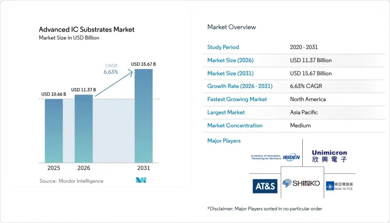
This report is Segmented by Substrate Type (Flip-Chip Ball Grid Array, Flip-Chip Chip Scale Package, and More), Core Material (Glass, Ceramic, and More), Packaging Technology (2D Flip-Chip, SiP/Module, and More), Device Node (Above 28nm, 7-5nm, and More), End-Use Industry (Mobile and Consumer, Data-Centre/AI and HPC, and More), and Geography. The Market Forecasts are Provided in Terms of Value (USD).
Global Advanced IC Substrates Market Trends and Insights
Surge in ABF-Substrate Demand for AI and HPC Accelerators
Hyperscale operators installed more than 1.2 million AI accelerator units in 2025, each integrating four to six flip-chip BGA substrates that must withstand power draw above 700 watts. Average selling prices climbed from USD 65 in 2024 to USD 82 in 2025 as coating-line additions lagged demand, widening suppliers' margins as they locked in Ajinomoto film allocations. Fabless chipmakers are now co-investing in substrate plants, illustrated by AMD's USD 400 million venture with Siliconware Precision Industries that secures 30% of a new Taiwanese facility's output. These forward-buy agreements squeeze mid-tier vendors that lack guaranteed slots, reinforcing a capacity oligopoly. As long as accelerator shipments double every 2 years, the advanced IC substrates market will continue to absorb incremental ABF panels at premium pricing.
Miniaturisation and Heterogeneous Integration Trend
Chiplet architectures slice monolithic dies into smaller compute, I/O, and memory tiles, cutting die area by up to 40% and enabling node-mixing strategies. Such layouts demand microvias below 50 micrometers and redistribution layers at 2 micrometer pitch, pushing both ABF and emerging glass cores to their physical limits. To stay design-win-relevant, Ibiden and AT&S embedded engineers at TSMC's packaging center 18 months ahead of tape-out, capturing 40% of the 2.5D interposer substrate pool by 2025. The collaboration model shifts substrate manufacturing from commodity production toward quasi-design services, accelerating learning curves and deepening vendor lock-in. Over the next decade, suppliers unable to align roadmaps with foundries risk relegation to legacy nodes, curtailing addressable revenue in the advanced IC substrates market.
ABF-Substrate Capacity Shortage and Lead-Time Spikes
Lead times for 14-layer ABF substrates stretched to 28 weeks in early 2025 as AI demand outran supply by 18 percentage points. Mid-tier fabless designers either paid spot premiums of 15-20% or postponed tape-outs by up to three quarters. Equipment chokepoints persist: LPKF Laser and Mitsubishi Electric hold roughly 70% of laser-drill capacity and face an 18-month delivery backlog. Large suppliers, therefore, over-book Ajinomoto film, amplifying scarcity for smaller rivals. Unless new coating lines come online before 2027, the advanced IC substrates market will remain capacity-constrained, trimming potential CAGR by an estimated 1.2 percentage points.
Other drivers and restraints analyzed in the detailed report include:
- 5G Roll-Out Boosting High-Frequency RF Packaging
- Co-Packaged Optics Adoption Requiring Ultra-Low-Loss Substrates
- High Capital Intensity and Process Complexity
For complete list of drivers and restraints, kindly check the Table Of Contents.
Segment Analysis
Flip-chip BGA commanded 43.89% of the advanced IC substrates market share in 2025, reflecting its entrenched position in mobile application processors and server CPUs. Rigid-flex and flexible CSP formats are advancing at a 7.71% CAGR through 2031, driven by smartwatches, augmented-reality headsets, and medical patches that benefit from bendable polyimide cores. Flip-chip CSP held 22% of 2025 shipment volume for ultra-thin smartphones, while organic BGA and LGA accounted for a steady 18% of volume in cost-focused automotive controllers. Other formats, including embedded-die and coreless substrates, accounted for the remaining 16%, driven by 5G millimeter-wave front-end modules that require improved thermal paths.
Chiplet-ready flip-chip BGA variants command 25-35% ASP premiums because multi-cavity layouts and fine redistribution layers raise manufacturing complexity. Suppliers with laser-direct-imaging and modified semi-additive processes secured roughly 70% of this high-margin pool, reshaping competitive balance. By contrast, panel-level processing helped rigid-flex yields, but the resulting 5% ASP erosion in 2025 pressured specialists to consolidate. The technology mix, therefore, tilts profitability toward advanced flip-chip formats even as unit growth skews toward flexible substrates, keeping product strategy nuanced across the advanced IC substrates market.
Ajinomoto build-up film captured 52.78% of 2025 revenue, reinforcing its status as the incumbent core for smartphones, PCs, and servers. Glass substrates are set for a 7.47% CAGR through 2031 as sub-4-nanometer logic and co-packaged optics demand ultra-low warpage and optical routing. Bismaleimide-triazine accounted for 15% of the volume in high-temperature automotive modules, while ceramic remained at 9% for RF power and LED packages. Hybrid glass-organic laminates under development could combine cost efficiency with glass-level flatness, challenging pure ABF beyond 2027.
Hyperscaler funding for Corning and AGC pilot lines may lift glass to 15-20% of premium server sockets by 2031, injecting fresh revenue into the advanced IC substrates market size. Automotive price-down pressure of 2-3% a year forces BT and ceramic vendors to automate inspection and test to protect margins. As a result, the long-term material strategy hinges on balancing ABF volume, glass performance, and BT cost discipline across diversified end uses.
Complete Report Scope:
- By Substrate Type
- Flip-Chip Ball Grid Array
- Flip-Chip Chip Scale Package
- Organic Ball Grid Array / Land Grid Array
- Rigid-Flex and Flexible Chip Scale Package
- Other Substrate Types
- By Core Material
- Ajinomoto Build-up Film
- Bismaleimide-Triazine Resin
- Glass
- Ceramic
- By Packaging Technology
- 2D Flip-Chip
- 2.5D Interposer
- 3D-IC / SoIC
- Fan-Out WLP
- SiP / Module
- By Device Node
- Above 28 nm
- 16/14-10 nm
- 7-5 nm
- 4 nm and below
- By End-Use Industry
- Mobile and Consumer
- Automotive and Transportation
- IT and Telecom Infrastructure
- Data-Centre / AI and HPC
- Other End-Use Industries
- By Geography
- North America
- United States
- Canada
- Mexico
- South America
- Brazil
- Argentina
- Rest of South America
- Europe
- United Kingdom
- Germany
- France
- Italy
- Rest of Europe
- Asia Pacific
- China
- Japan
- India
- South Korea
- Rest of Asia Pacific
- Middle East and Africa
- Middle East
- United Arab Emirates
- Saudi Arabia
- Rest of Middle East
- Africa
- South Africa
- Egypt
- Rest of Africa
- Middle East
- North America
Geography Analysis
Asia-Pacific accounted for 78.36% of the advanced IC substrates market size in 2025, anchored by Taiwan's 420 million flip-chip BGA shipments and Japan's specialization in 14-layer and 16-layer server substrates. South Korean vendors raised rigid-flex output to 85 million units and achieved cost parity with strip formats by switching to panel processing. Chinese suppliers increased legacy-node capacity and priced 10-15% below Taiwanese averages, boosting their share of automotive and industrial demand to 18%. India remained a nascent player, as pilot lines at Tata Electronics and Kaynes Technology shipped fewer than 5 million substrates due to yield challenges.
North America is projected to expand at a 7.69% CAGR through 2031, propelled by USD 2.8 billion in CHIPS Act incentives tied to domestic substrate and packaging plants. Ibiden's USD 1.2 billion Arizona fab and AT&S's USD 800 million Texas facility will together add 50,000 panels per month after 2027, giving U.S. fabless firms a second sourcing hub. Mexican near-shoring added 22 million units in 2025 as Tripod Technology and Zhen Ding Technology enlarged Guadalajara operations to serve automotive and industrial customers. Dual-sourcing clauses in U.S. contracts are already fragmenting order volumes, pressuring Asian incumbents to establish North American subsidiaries to defend their share.
Europe accounted for 6% of 2025 revenue, concentrated in Austria and Germany, where AT&S and Schweizer Electronic cater to automotive and industrial clients. AT&S's Leoben expansion, backed by EUR 500 million in EU Chips funds, will bring 20,000 additional FC-BGA panels per month starting in 2027. South America, the Middle East, and Africa together accounted for less than 2%, reflecting limited semiconductor assembly capacity and long payback periods for greenfield fabs. Unless subsidy frameworks emerge to offset high capital costs, these regions will remain fringe participants in the advanced IC substrates market.
- Unimicron Technology Corp.
- Ibiden Co., Ltd.
- Nan Ya Printed Circuit Board Corp.
- Shinko Electric Industries Co., Ltd.
- AT&S Austria Technologie & Systemtechnik AG
- Kinsus Interconnect Technology Corp.
- Samsung Electro-Mechanics Co., Ltd.
- Kyocera Corporation
- ASE Technology Holding Co., Ltd.
- LG Innotek Co., Ltd.
- Simmtech Co., Ltd.
- TTM Technologies, Inc.
- Fujitsu Interconnect Technologies Ltd.
- JCET Group Co., Ltd.
- Panasonic Holdings Corporation
- Zhen Ding Technology Holding Ltd.
- Shennan Circuits Co., Ltd.
- Daeduck Electronics Co., Ltd.
- WUS Printed Circuit Co., Ltd.
- Zhejiang Kingdom Sci-Tech Co., Ltd.
- SKC Absolics Inc.
- Tripod Technology Corp.
- Toppan Inc.
Additional Benefits:
- The market estimate (ME) sheet in Excel format
- 3 months of analyst support
TABLE OF CONTENTS
1 INTRODUCTION
- 1.1 Study Assumptions and Market Definition
- 1.2 Scope of the Study
2 RESEARCH METHODOLOGY
3 EXECUTIVE SUMMARY
4 MARKET LANDSCAPE
- 4.1 Market Overview
- 4.2 Market Drivers
- 4.2.1 Surge in ABF-Substrate Demand for AI and HPC Accelerators
- 4.2.2 Miniaturisation and Heterogeneous Integration Trend
- 4.2.3 5G Roll-Out Boosting High-Frequency RF Packaging
- 4.2.4 Co-Packaged Optics Adoption Requiring Ultra-Low-Loss Substrates
- 4.2.5 CHIPS-Style Localisation Subsidies Tied to Substrate Fabs
- 4.2.6 Large-Panel Organic Substrate Lines Lowering Cost Per Die
- 4.3 Market Restraints
- 4.3.1 ABF-Substrate Capacity Shortage and Lead-Time Spikes
- 4.3.2 High Capital Intensity and Process Complexity
- 4.3.3 Single-Source Dependency on ABF Build-Up Films
- 4.3.4 Stricter Fluorinated-Solvent Emission Regulations
- 4.4 Industry Value Chain Analysis
- 4.5 Regulatory Landscape
- 4.6 Technological Outlook
- 4.7 Porter's Five Forces Analysis
- 4.7.1 Bargaining Power of Suppliers
- 4.7.1.1 Bargaining Power of Consumers
- 4.7.1.2 Threat of New Entrants
- 4.7.1.3 Threat of Substitutes
- 4.7.1.4 Intensity of Competitive Rivalry
- 4.7.1 Bargaining Power of Suppliers
- 4.8 Pricing Analysis
- 4.9 Impact of Macroeconomic Factors
5 MARKET SIZE AND GROWTH FORECASTS (VALUE)
- 5.1 By Substrate Type
- 5.1.1 Flip-Chip Ball Grid Array
- 5.1.2 Flip-Chip Chip Scale Package
- 5.1.3 Organic Ball Grid Array / Land Grid Array
- 5.1.4 Rigid-Flex and Flexible Chip Scale Package
- 5.1.5 Other Substrate Types
- 5.2 By Core Material
- 5.2.1 Ajinomoto Build-up Film
- 5.2.2 Bismaleimide-Triazine Resin
- 5.2.3 Glass
- 5.2.4 Ceramic
- 5.3 By Packaging Technology
- 5.3.1 2D Flip-Chip
- 5.3.2 2.5D Interposer
- 5.3.3 3D-IC / SoIC
- 5.3.4 Fan-Out WLP
- 5.3.5 SiP / Module
- 5.4 By Device Node
- 5.4.1 Above 28 nm
- 5.4.2 16/14-10 nm
- 5.4.3 7-5 nm
- 5.4.4 4 nm and below
- 5.5 By End-Use Industry
- 5.5.1 Mobile and Consumer
- 5.5.2 Automotive and Transportation
- 5.5.3 IT and Telecom Infrastructure
- 5.5.4 Data-Centre / AI and HPC
- 5.5.5 Other End-Use Industries
- 5.6 By Geography
- 5.6.1 North America
- 5.6.1.1 United States
- 5.6.1.2 Canada
- 5.6.1.3 Mexico
- 5.6.2 South America
- 5.6.2.1 Brazil
- 5.6.2.2 Argentina
- 5.6.2.3 Rest of South America
- 5.6.3 Europe
- 5.6.3.1 United Kingdom
- 5.6.3.2 Germany
- 5.6.3.3 France
- 5.6.3.4 Italy
- 5.6.3.5 Rest of Europe
- 5.6.4 Asia Pacific
- 5.6.4.1 China
- 5.6.4.2 Japan
- 5.6.4.3 India
- 5.6.4.4 South Korea
- 5.6.4.5 Rest of Asia Pacific
- 5.6.5 Middle East and Africa
- 5.6.5.1 Middle East
- 5.6.5.1.1 United Arab Emirates
- 5.6.5.1.2 Saudi Arabia
- 5.6.5.1.3 Rest of Middle East
- 5.6.5.2 Africa
- 5.6.5.2.1 South Africa
- 5.6.5.2.2 Egypt
- 5.6.5.2.3 Rest of Africa
- 5.6.5.1 Middle East
- 5.6.1 North America
6 COMPETITIVE LANDSCAPE
- 6.1 Market Concentration
- 6.2 Strategic Moves
- 6.3 Market Share Analysis
- 6.4 Company Profiles (includes Global Level Overview, Market Level Overview, Core Segments, Financials as available, Strategic Information, Market Rank/Share, Products and Services, Recent Developments)
- 6.4.1 Unimicron Technology Corp.
- 6.4.2 Ibiden Co., Ltd.
- 6.4.3 Nan Ya Printed Circuit Board Corp.
- 6.4.4 Shinko Electric Industries Co., Ltd.
- 6.4.5 AT&S Austria Technologie & Systemtechnik AG
- 6.4.6 Kinsus Interconnect Technology Corp.
- 6.4.7 Samsung Electro-Mechanics Co., Ltd.
- 6.4.8 Kyocera Corporation
- 6.4.9 ASE Technology Holding Co., Ltd.
- 6.4.10 LG Innotek Co., Ltd.
- 6.4.11 Simmtech Co., Ltd.
- 6.4.12 TTM Technologies, Inc.
- 6.4.13 Fujitsu Interconnect Technologies Ltd.
- 6.4.14 JCET Group Co., Ltd.
- 6.4.15 Panasonic Holdings Corporation
- 6.4.16 Zhen Ding Technology Holding Ltd.
- 6.4.17 Shennan Circuits Co., Ltd.
- 6.4.18 Daeduck Electronics Co., Ltd.
- 6.4.19 WUS Printed Circuit Co., Ltd.
- 6.4.20 Zhejiang Kingdom Sci-Tech Co., Ltd.
- 6.4.21 SKC Absolics Inc.
- 6.4.22 Tripod Technology Corp.
- 6.4.23 Toppan Inc.
7 MARKET OPPORTUNITIES AND FUTURE OUTLOOK
- 7.1 White-Space and Unmet-Need Assessment