
|
시장보고서
상품코드
2125753
자동 광학 검사 장비 시장 : 시장 점유율 분석, 업계 동향 및 통계, 성장 예측(2026-2031년)Automated Optical Inspection Equipment - Market Share Analysis, Industry Trends & Statistics, Growth Forecasts (2026 - 2031) |
||||||
 Mordor Intelligence
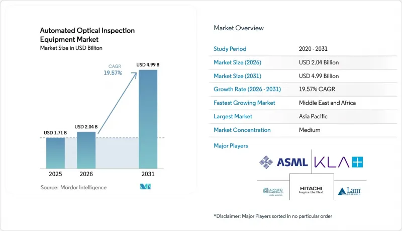
Mordor Intelligence에 의하면, 자동 광학 검사 장비 시장 규모는 2025년에 17억 1,000만 달러로 평가되었고, 2026년 20억 4,000만 달러에서 2031년까지 49억 9,000만 달러에 이를 것으로 예측되며, 예측 기간(2026-2031년) CAGR은 19.57%를 나타낼 전망입니다.
본 보고서는 제품 유형별(2D AOI 시스템, 3D AOI 시스템), 기술별(인라인 시스템, 오프라인/데스크톱 시스템), 구성 요소별(하드웨어, 소프트웨어/AI 알고리즘), 최종 이용 산업별(반도체 제조, PCB 및 EMS 공급업체, 가전제품 조립, 기타), 지역별로 분류되어 있습니다. 시장 예측은 금액(달러) 기준으로 제시되어 있습니다.
세계의 자동 광학 검사 장비 시장 동향 및 인사이트
고밀도·소형화된 PCB에 대한 수요 증가
부품의 실적는 0402 패키지에서 0201 패키지로 축소되었으며, 현재는 01005 패키지로 전환되고 있는 가운데, 생산 타크트 타임은 변함없이 유지되면서 검사 해상도는 10 마이크로미터 미만이 요구되고 있습니다. TRI의 TR7700Q SII 플랫폼은 파워트레인용 PCB의 제로 에스케이프 검사를 위해 동기화된 멀티 카메라 3D 이미징을 도입하여 1마이크로미터의 해상도를 실현했습니다. 테슬라(Tesla)가 안전상 중요한 제어 기판에 대해 차세대 AOI 인증을 획득한 것에서도 알 수 있듯이, 자동차 제조업체들은 배터리 관리 어셈블리를 보호하기 위해 이러한 기능을 채택하고 있습니다. 마찬가지로, 의료용 임플란트 제조업체들도 제품 승인을 확보하기 위해 10마이크로미터 이하의 검사 범위를 의무화하고 있으며, 5G 무선 기판의 경우 mm파 신호의 무결성을 보장하기 위해 공극이 없는 솔더 충진이 요구되고 있습니다. 이러한 요구 사항이 수렴됨에 따라, Tier 1 및 Tier 2 EMS 거점에서는 기존 2D 검사 장비에서 고정밀 3D 플랫폼으로의 전환이 가속화되고 있습니다.
2D에서 진정한 3D 검사 기능으로의 전환
기존 2D 시스템에서는 BGA나 칩 스케일 패키지 아래의 공면성이나 솔더 볼의 부피를 정량화할 수 없기 때문에 현장 서비스 시 잠재적인 결함이 발생할 수 있습니다. Omron의 VT-S1080은 다방향·다색 조명을 채택함으로써 셋업 시간을 70% 단축하는 동시에 체적 측정 정밀도를 반도체 등급 수준으로 향상시켰습니다. KLA는 이 개념을 첨단 패키징 부문으로 확대하여, 2025 회계연도 2분기 매출 30억 8,000만 달러의 일부를 칩렛 브리지 및 실리콘 관통 비아(TSV)의 보이드 문제를 해결하는 3D 측정 기술의 연구 개발에 투입하고 있습니다. 인라인 3D 피드백을 통해 스텐실의 자동 세척 및 솔더 페이스트 도포 보정이 자동으로 이루어지게 되어, 이로 인해 첫 번째 통과율이 향상되고 다운스트림 공정에서의 X선 검증을 최소화할 수 있습니다. 따라서 기판의 고밀도화가 진행됨에 따라 시장은 계속해서 3D AOI로 전환되고 있습니다.
인라인 3D AOI의 고액 설비 투자와 통합의 복잡성
인라인 3D 스테이션의 비용은 레인당 50만-200만 달러이며, 고정밀 컨베이어, 환경 격리, MES와의 연동이 필요합니다. IPC의 조사에 따르면, 반도체 부족이 장기화되는 가운데 기판 제조업체의 90%가 평균 14.5%의 투입 비용 상승에 직면하고 있어, 설비 투자 여지는 제한적입니다. 그 결과, 소규모 EMS 제조업체들은 설비 교체를 미루고 다품종 대량 생산 라인에 대응할 수 없는 오프라인 데스크사이드형 장비에 의존하고 있어, 도입 현황에 양극화가 지속되고 있습니다. 또한, 시스템 통합에는 숙련된 기술자와 예비 부품이 필요하며, 그 결과 총 소유 비용이 당초 견적을 초과하게 됩니다. 이로 인해 소량 생산 제조업체의 경우 투자 회수 기간이 3년 이상 지연될 가능성이 있습니다.
부문 분석
3D 플랫폼은 2025년 매출의 56.72%를 차지했으며, 자동 광학 검사 장비 시장이 라인 속도 기반의 체적 측정으로 전환되고 있음을 반영합니다. 이 점유율은 반도체 및 자동차 산업 고객들이 2D 장비로는 이용할 수 없는 공평면성 검증 및 페이스트 높이 분석을 요구함에 따라 상승했습니다. 3D 시스템에 기인한 자동 광학 검사 장비 시장 규모는 칩렛 조립에서 패드 피치의 축소에 힘입어 2031년까지 연평균 성장률(CAGR) 13.86%로 확대될 것으로 예측됩니다. 2D 시스템은 표면 수준의 흠집이나 극성 확인으로 충분한 가전제품 부문, 특히 극한의 처리량을 추구하는 수탁 제조 공장에서 여전히 중요한 역할을 하고 있습니다.
센서 가격 하락과 알고리즘 라이브러리의 성숙에 따라 2D와 3D의 비용 격차는 점차 줄어들고 있습니다. 프라운호퍼 연구소의 SURFinpro 프로토타입은 AI를 활용하여 더 적은 수의 카메라로도 솔더의 형상을 재구성할 수 있음을 입증함으로써, 부품 원가를 절감하면서도 3D에 버금가는 정밀도에 근접할 수 있게 되었습니다. 그 결과, 도입이 늦어졌던 EMS 기업에서도 ROI가 향상되었으며, 이에 따라 기존 2D 라인의 폐지가 가속화되고 있습니다. 또한, 공정 분석을 통해 페이스트 양의 측정값과 스텐실 세척 주기가 연동되게 됨에 따라, 사업자는 불량품 및 보증 반품을 줄이기 위한 실용적인 데이터를 확보할 수 있게 되었습니다.
인라인 장비는 하류 조립 공정 전에 결함을 격리하는 폐쇄 루프 피드백을 제공함으로써 2025년에는 62.75%의 점유율을 확보했습니다. 인더스트리 4.0 파일럿 프로젝트가 공장 전체로 확대됨에 따라, 자동 광학 검사 장비 시장에서 인라인 장비의 출하 대수는 연평균 성장률(CAGR) 11.74%로 확대될 것으로 예측됩니다. 검사 프레임 내에 장착된 엣지 서버를 통해 모델을 로컬에서 실행할 수 있으므로, 페이스트 인쇄의 오프셋이 운영자의 개입 없이 프린터 조정을 촉발합니다.
오프라인/데스크톱형 장비는 고배율 광학 시스템 하에서 장시간 노출이 필요한 소량 생산 의료용 및 항공우주용 기판에 계속해서 활용되고 있습니다. 이러한 시스템은 인라인 도입에 따른 설비 투자(CAPEX)를 주저하던 중소기업들 사이에서 다시 주목받고 있습니다. 그러나 기업의 MES 제품군이 AOI 이미지를 가져와 스텐실 마모를 예측하거나 감사 담당자가 승인하는 Cpk 지표를 도출할 수 있게 됨에 따라 인라인의 우위는 더욱 높아지고 있습니다. 그 결과, 북미, 유럽 및 선진 아시아태평양의 공장에서는 라인 설계자들이 새로운 표면 실장 라인의 표준 사양으로 인라인 AOI를 지정하고 있습니다.
지역별 분석
아시아태평양은 중국의 490억 달러에 달하는 반도체 제조 장비 투자와 TSMC가 주도하는 대만의 패널 레벨 패키징(PLP) 프로젝트를 배경으로, 2025년 매출의 56.65%를 계속 차지했습니다. 아시아태평양의 자동 광학 검사 장비 시장 규모는 여전히 방대하지만, 정책 리스크와 임금 상승으로 인해 일부 OEM 업체들은 베트남, 인도, 말레이시아로 사업을 다각화함에 따라 새로운 AOI 수주가 지역 전체에 분산되는 결과를 낳았습니다. 일본의 성숙한 자동차용 전자기기 산업은 SiC 인버터 보드의 방열판 평면도를 검증하는 3D 계측 라인에 대한 투자를 지속했습니다.
북미 시장 점유율은 확대되었습니다. 이는 ‘CHIPS법’에 따른 보조금 및 현지 조달 정책으로 인해 각 팹 업체들이 인라인 검사 장비를 국내에서 조달하게 되었기 때문입니다. 미국의 장비에 대한 설비 투자액은 2027년에 247억 달러에 달할 것으로 예측되며, AOI의 수주 잔고는 견조한 추세를 보일 것으로 예상되지만, 약 8만 명에 달하는 기술자 부족이 노동력 부족을 초래하여 생산 능력을 제약할 가능성이 있습니다. 멕시코는 USMCA에 따른 파급 효과로 EMS 계약을 수주했으며, 이에 따라 AOI 벤더 각사는 니어쇼어링 생산 라인을 지원하기 위해 누에보 레온 주에 서비스 센터를 개설했습니다.
유럽은 기술적 자립을 추구하며, 기후 정책 자금을 전력 소비를 20% 절감하는 에너지 효율이 높은 AOI 모듈에 배정했습니다. 독일의 1차 자동차 부품 공급업체는 실리콘 카바이드 파워 모듈용 라인 스캔 방식의 3D 장비를 발주한 반면, 북유럽의 스타트업 기업은 기가팩토리에서 배터리 셀 탭 검사에 AI 기반 AOI를 도입했습니다. 브렉시트로 인한 공급망의 복잡화로 통관 절차가 증가했으나, 네덜란드에 설치된 현지 재고 거점을 통해 EU 고객에 대한 리드 타임이 단축되었습니다.
중동 및 아프리카는 규모는 아직 작지만, 산업 다각화 정책을 추진하는 각국 정부가 세제 우대 조치를 통해 PCB 조립 업체와 LED 조명 제조업체를 유치한 결과, 13.92%라는 가장 높은 연평균 성장률(CAGR)이 예상됩니다. 리야드 근교에 위치한 사우디아라비아의 전자기기 제조 회랑에서는 0201 사이즈 검사가 가능한 엔트리 레벨 인라인 AOI가 첫 주문되었으며, 기술력 향상에 따라 향후 3D로 업그레이드될 것으로 예측됩니다.
기타 혜택
- 엑셀 형식 시장 예측(ME) 시트
- 3개월간의 애널리스트 지원
자주 묻는 질문
목차
제1장 서론
제2장 조사 방법
제3장 주요 요약
제4장 시장 구도
제5장 시장 규모 및 성장 예측
제6장 경쟁 구도
제7장 시장 기회 및 향후 전망
AJY 26.09.15According to Mordor Intelligence, the automated optical inspection equipment market size was valued at USD 1.71 billion in 2025 and estimated to grow from USD 2.04 billion in 2026 to reach USD 4.99 billion by 2031, at a CAGR of 19.57% during the forecast period (2026-2031).
This report is Segmented by Product Type (2D AOI Systems, 3D AOI Systems), Technology (Inline Systems, Offline/Desktop Systems), Component (Hardware, Software/AI Algorithms), End-Use Industry (Semiconductor Manufacturing, PCB and EMS Providers, Consumer Electronics Assembly, and More), and Geography. The Market Forecasts are Provided in Terms of Value (USD).
Global Automated Optical Inspection Equipment Market Trends and Insights
Increasing Demand for High-Density, Miniaturized PCBs
Component footprints shrank from 0402 to 0201 packages and are now moving toward 01005, forcing inspection resolutions below 10 µm while production takt times remain unchanged. TRI's TR7700Q SII platform demonstrated 1 µm resolution by deploying synchronized multi-camera 3D imaging for zero-escape inspection of power-train PCBs. Automakers adopted such capability to protect battery-management assemblies, as evidenced by Tesla's qualification of next-generation AOI on its safety-critical control boards. Medical-implant makers likewise mandated sub-10 µm coverage to secure product approvals, and 5G radio boards now require void-free solder volumes to assure mmWave signal integrity. These converging needs are accelerating replacement of legacy 2D stations with high-precision 3D platforms across both tier-one and tier-two EMS sites.
Transition from 2D to True-3D Inspection Capability
Legacy 2D systems cannot quantify coplanarity or solder-ball volume under BGAs and chip-scale packages, which leads to latent defects in field service. Omron's VT-S1080 adopted Multi-Direction Multi-Color illumination to reduce setup time by 70% while raising volumetric accuracy to semiconductor-grade thresholds. KLA extended the concept to advanced packaging, channeling a portion of its USD 3.08 billion Q2 FY 2025 revenue into 3D metrology R&D that addresses chiplet bridges and through-silicon via voids. Inline 3D feedback now triggers automatic stencil cleaning or solder-paste deposition correction, which increases first-pass yield and minimizes downstream X-ray verification. The market therefore continues to migrate toward 3D AOI as board densities climb.
High CAPEX and Integration Complexity of Inline 3D AOI
An inline 3D station costs USD 500,000-2 million per lane and demands precision conveyors, environmental isolation and MES interfacing. IPC surveys showed 90% of board houses contended with input-cost spikes averaging 14.5% as semiconductor shortages lingered, leaving limited headroom for capital purchases. Small EMS shops therefore postpone upgrades and rely on offline deskside units that cannot keep pace with high-mix high-volume lines, perpetuating a two-tier adoption pattern. Integration also requires trained technicians and spare parts, bringing total cost of ownership above initial quotations, which can delay ROI beyond three years for low-volume manufacturers.
Other drivers and restraints analyzed in the detailed report include:
- Rapid Adoption of AI-Enabled Adaptive Learning Algorithms
- Electronics Manufacturing Reshoring in North America and Europe
- Trade-Compliance Barriers on Imaging Sensors and Lasers
For complete list of drivers and restraints, kindly check the Table Of Contents.
Segment Analysis
3D platforms generated 56.72% of 2025 revenue, reflecting the automated optical inspection equipment market's pivot to volumetric measurement at line speeds. That share rose as semiconductor and automotive clients demanded co-planarity verification and paste-height analytics unavailable on 2D gear. The automated optical inspection equipment market size attributed to 3D systems is projected to climb at 13.86% CAGR through 2031, propelled by shrinking pad pitches in chiplet assemblies. 2D variants remain relevant for consumer electronics where surface-level scratch and polarity checks suffice, especially in contract factories pursuing extreme throughput.
The cost gap between 2D and 3D is narrowing as sensor prices fall and algorithm libraries mature. Fraunhofer's SURFinpro prototype proved that AI can reconstruct solder geometries with fewer cameras, trimming bill-of-material cost while approaching 3D accuracy. As a result, late-adopter EMS firms see improved ROI, which accelerates the retirement of legacy 2D lines. Because process analytics now tie paste-volume readings to stencil-cleaning cycles, operators gain actionable data that curtails scrap and warranty returns.
Inline machines secured 62.75% share in 2025 by providing closed-loop feedback that quarantines defects before downstream assembly. Inline shipments within the automated optical inspection equipment market are forecast to advance at 11.74% CAGR as Industry 4.0 pilots transition to plant-wide rollouts. Edge servers housed inside the inspection frame let models run locally so that paste-print offsets trigger printer adjustments without operator intervention.
Offline/desktop units continue to serve low-volume medical or aerospace boards requiring extended dwell time under high-magnification optics. These systems saw renewed interest among small businesses deterred by inline CAPEX. Yet the inline advantage has grown as enterprise MES suites now ingest AOI images to predict stencil wear and derive Cpk indicators that auditors accept. Consequently, line designers specify inline AOI as standard for new surface-mount tracks across North America, Europe and progressive APAC factories.
Complete Report Scope:
- By Product Type
- 2D AOI Systems
- 3D AOI Systems
- By Technology
- Inline Systems
- Offline / Desktop Systems
- By Component
- Hardware (Cameras, Illumination, Controllers)
- Software / AI Algorithms
- By End-use Industry
- Semiconductor Manufacturing
- PCB and EMS Providers
- Consumer Electronics Assembly
- Automotive Electronics
- Solar and Battery Manufacturing
- Medical Devices
- Aerospace and Defense Electronics
- By Geography
- North America
- United States
- Canada
- Mexico
- South America
- Brazil
- Argentina
- Rest of South America
- Europe
- Germany
- United Kingdom
- France
- Italy
- Russia
- Rest of Europe
- Asia-Pacific
- China
- Japan
- South Korea
- India
- ASEAN
- Rest of Asia-Pacific
- Middle East and Africa
- Middle East
- Saudi Arabia
- United Arab Emirates
- Turkey
- Rest of Middle East
- Africa
- South Africa
- Nigeria
- Rest of Africa
- Middle East
- North America
Geography Analysis
Asia-Pacific retained 56.65% of 2025 revenue on the strength of China's USD 49 billion semiconductor-equipment outlays and Taiwan's panel-level packaging projects led by TSMC. The automated optical inspection equipment market size attributed to Asia-Pacific remains substantial, yet policy risk and rising wages spurred some OEMs to diversify into Vietnam, India and Malaysia, dispersing new AOI orders across the region. Japan's mature automotive electronics base continued investing in 3D metrology lines that validate heat-sink coplanarity for SiC inverter boards.
North America's share expanded as CHIPS Act grants and local procurement policies drove fabs to source inline inspection domestically. Capital spending on US equipment is projected to reach USD 24.7 billion in 2027, ensuring steady AOI backlog, although an estimated 80,000 unfilled technician posts could constrain throughput if workforce.. Mexico captured spill-over EMS contracts under USMCA, prompting AOI vendors to open service centers in Nuevo Leon to support near-shoring lines.
Europe pursued technological self-reliance, channeling climate-policy funds toward energy-efficient AOI modules that cut power draw by 20%. Germany's Tier-1 auto suppliers ordered line-scan 3D units for silicon-carbide power modules, while Nordic start-ups adopted AI-based AOI for battery-cell tabs in gigafactories. Supply-chain complexity following Brexit added customs paperwork, but localized inventory pools in the Netherlands trimmed lead-times for EU customers.
Middle East and Africa, though still small, recorded the fastest 13.92% CAGR outlook as governments under industrial-diversification agendas lured PCB assemblers and LED lighting producers with tax incentives. Saudi Arabia's electronic-manufacturing corridor near Riyadh placed initial orders for entry-level inline AOI capable of 0201 inspection, signaling future upgrades to 3D as skill levels rise.
- KLA Corporation
- Koh Young Technology Inc.
- Omron Corporation
- Saki Corporation
- Nordson Corporation (CyberOptics)
- Test Research, Inc. (TRI)
- Mirtec Co., Ltd.
- Viscom AG
- Camtek Ltd.
- Hitachi High-Tech Corporation
- Applied Materials, Inc.
- ASML Holding N.V.
- Lam Research Corporation
- JUTZE Intelligence Technology Co., Ltd.
- Goepel Electronic GmbH
- Mek (Marantz Electronics)
- Chroma ATE Inc.
- ViTrox Corp. Berhad
- PARMI Co., Ltd.
- Pemtron Corporation
- Orbotech (KLA)
- VI-Technology (Mycronic)
- Machine Vision Products, Inc. (MVP)
- ALeader Tech Co., Ltd.
- TechValley Co., Ltd.
Additional Benefits:
- The market estimate (ME) sheet in Excel format
- 3 months of analyst support
TABLE OF CONTENTS
1 INTRODUCTION
- 1.1 Study Assumptions and Market Definition
- 1.2 Scope of the Study
2 RESEARCH METHODOLOGY
3 EXECUTIVE SUMMARY
4 MARKET LANDSCAPE
- 4.1 Market Overview
- 4.2 Market Drivers
- 4.2.1 Increasing demand for high-density, miniaturized PCBs
- 4.2.2 Transition from 2D to true-3D inspection capability
- 4.2.3 Rapid adoption of AI-enabled adaptive learning algorithms
- 4.2.4 Post-COVID reshoring of electronics manufacturing in North America and Europe
- 4.2.5 Edge-computing AOI for real-time process correction (under-the-radar)
- 4.2.6 Growth of chiplet and advanced-packaging lines needing sub-10 m inspection (under-the-radar)
- 4.3 Market Restraints
- 4.3.1 High CAPEX and integration complexity of inline 3D AOI
- 4.3.2 Short product lifecycles demanding frequent re-programming
- 4.3.3 Limited availability of AOI-talent for AI data-labelling (under-the-radar)
- 4.3.4 Trade-compliance barriers on imaging sensors and lasers (under-the-radar)
- 4.4 Impact of Macroeconomic Factors
- 4.5 Value Chain Analysis
- 4.6 Regulatory Landscape
- 4.7 Technological Outlook
- 4.8 Ecosystem Analysis
- 4.9 Porters Five Forces Analysis
- 4.9.1 Bargaining Power of Suppliers
- 4.9.2 Bargaining Power of Buyers
- 4.9.3 Threat of New Entrants
- 4.9.4 Threat of Substitutes
- 4.9.5 Intensity of Competitive Rivalry
5 MARKET SIZE AND GROWTH FORECASTS (VALUE)
- 5.1 By Product Type
- 5.1.1 2D AOI Systems
- 5.1.2 3D AOI Systems
- 5.2 By Technology
- 5.2.1 Inline Systems
- 5.2.2 Offline / Desktop Systems
- 5.3 By Component
- 5.3.1 Hardware (Cameras, Illumination, Controllers)
- 5.3.2 Software / AI Algorithms
- 5.4 By End-use Industry
- 5.4.1 Semiconductor Manufacturing
- 5.4.2 PCB and EMS Providers
- 5.4.3 Consumer Electronics Assembly
- 5.4.4 Automotive Electronics
- 5.4.5 Solar and Battery Manufacturing
- 5.4.6 Medical Devices
- 5.4.7 Aerospace and Defense Electronics
- 5.5 By Geography
- 5.5.1 North America
- 5.5.1.1 United States
- 5.5.1.2 Canada
- 5.5.1.3 Mexico
- 5.5.2 South America
- 5.5.2.1 Brazil
- 5.5.2.2 Argentina
- 5.5.2.3 Rest of South America
- 5.5.3 Europe
- 5.5.3.1 Germany
- 5.5.3.2 United Kingdom
- 5.5.3.3 France
- 5.5.3.4 Italy
- 5.5.3.5 Russia
- 5.5.3.6 Rest of Europe
- 5.5.4 Asia-Pacific
- 5.5.4.1 China
- 5.5.4.2 Japan
- 5.5.4.3 South Korea
- 5.5.4.4 India
- 5.5.4.5 ASEAN
- 5.5.4.6 Rest of Asia-Pacific
- 5.5.5 Middle East and Africa
- 5.5.5.1 Middle East
- 5.5.5.1.1 Saudi Arabia
- 5.5.5.1.2 United Arab Emirates
- 5.5.5.1.3 Turkey
- 5.5.5.1.4 Rest of Middle East
- 5.5.5.2 Africa
- 5.5.5.2.1 South Africa
- 5.5.5.2.2 Nigeria
- 5.5.5.2.3 Rest of Africa
- 5.5.5.1 Middle East
- 5.5.1 North America
6 COMPETITIVE LANDSCAPE
- 6.1 Market Concentration
- 6.2 Strategic Moves
- 6.3 Market Share Analysis
- 6.4 Company Profiles (includes Global level Overview, Market level overview, Core Segments, Financials as available, Strategic Information, Market Rank/Share, Products and Services, Recent Developments)
- 6.4.1 KLA Corporation
- 6.4.2 Koh Young Technology Inc.
- 6.4.3 Omron Corporation
- 6.4.4 Saki Corporation
- 6.4.5 Nordson Corporation (CyberOptics)
- 6.4.6 Test Research, Inc. (TRI)
- 6.4.7 Mirtec Co., Ltd.
- 6.4.8 Viscom AG
- 6.4.9 Camtek Ltd.
- 6.4.10 Hitachi High-Tech Corporation
- 6.4.11 Applied Materials, Inc.
- 6.4.12 ASML Holding N.V.
- 6.4.13 Lam Research Corporation
- 6.4.14 JUTZE Intelligence Technology Co., Ltd.
- 6.4.15 Goepel Electronic GmbH
- 6.4.16 Mek (Marantz Electronics)
- 6.4.17 Chroma ATE Inc.
- 6.4.18 ViTrox Corp. Berhad
- 6.4.19 PARMI Co., Ltd.
- 6.4.20 Pemtron Corporation
- 6.4.21 Orbotech (KLA)
- 6.4.22 VI-Technology (Mycronic)
- 6.4.23 Machine Vision Products, Inc. (MVP)
- 6.4.24 ALeader Tech Co., Ltd.
- 6.4.25 TechValley Co., Ltd.
7 MARKET OPPORTUNITIES AND FUTURE OUTLOOK
- 7.1 White-space and Unmet-need Assessment