|
시장보고서
상품코드
1479763
서브 100nm 리소그래피 : 세계 시장 분석과 전략적 과제Sub-100nm Lithography: Market Analysis and Strategic Issues |
||||||
촉진요인
반도체 기술의 노드가 축소되고 더 작고 복잡한 반도체 디바이스에 대한 수요가 증가함에 따라 여러 가지 촉진요인이 이러한 과제를 해결하기 위한 리소그래피 기술의 발전을 촉진하고 있습니다.
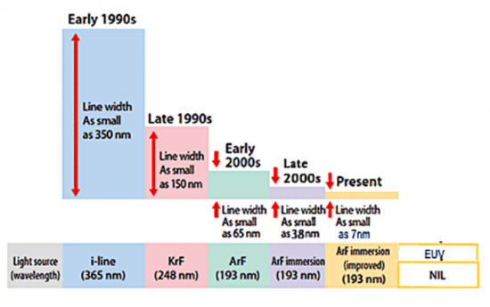
기술의 미세화: 새로운 기술 노드가 등장할 때마다 반도체 제조업체들은 성능, 전력 효율, 밀도를 향상시키기 위해 트랜지스터와 배선 크기를 줄이는 것을 목표로 하고 있습니다. 이러한 미세화를 높은 정밀도와 고해상도로 구현하기 위해서는 첨단 리소그래피 기술이 필수적이며, 이를 위해 차세대 리소그래피 툴의 개발이 추진되고 있습니다.
EUV 리소그래피 채택: EUV 리소그래피는 기존의 광학 리소그래피보다 파장이 짧아 더 미세하고 복잡한 패턴을 형성할 수 있습니다. 노드의 미세화에 따라 필요한 패터닝 해상도를 달성하기 위해 EUV 리소그래피의 채택이 점점 더 필요하게 되었습니다.

멀티패터닝 기술: 피처 크기가 광학 리소그래피의 한계에 가까워짐에 따라 SADP, SAQP, MBML과 같은 멀티패터닝 기술은 원하는 피처 밀도와 피치를 달성하는 데 필수적입니다. 이러한 기술들은 복잡한 패턴을 형성하기 위해 여러 번의 노광 및 에칭 공정이 필요하기 때문에 첨단 리소그래피 솔루션의 필요성이 증가하고 있습니다.
해상도 향상 기술(RET) : 패턴 전사의 해상도와 충실도를 향상시키기 위해 리소그래피 툴은 광학 근접 효과 보정(OPC), 위상 시프트 마스크(PSM), 소스 마스크 최적화(SMO)와 같은 해상도 향상 기술을 내장하고 있습니다. 이러한 RET는 회절 및 기타 광학 제한의 영향을 완화하여 첨단 노드에서 더 미세한 피처를 제작할 수 있도록 돕습니다.
공정 제어 및 수율 개선: 피처 크기가 작아짐에 따라 엄격한 공정 제어를 유지하는 것이 점점 더 어려워지고 있습니다. 고급 리소그래피 툴에는 균일성, 오버레이 정확도 및 결함 감소를 보장하기 위한 고급 측정 및 공정 제어 기능이 내장되어 있습니다. 이러한 기능은 첨단 노드에서 높은 수율과 제조 일관성을 달성하는 데 필수적입니다.
신흥 용도 및 시장 수요: AI, 5G 커넥티비티, 자율주행차, IoT 장비와 같은 신기술은 특정 성능 요건을 갖춘 특수 반도체 장비에 대한 수요를 촉진하고 있습니다. 첨단 리소그래피 솔루션은 이러한 용도에 필요한 복잡한 구조와 재료를 패터닝하는 데 필수적이며, 리소그래피 기술의 혁신을 촉진하고 있습니다.
이 보고서의 필요성
반도체 리소그래피는 반도체 제조의 초석이며, 현대의 전자제품을 지원하는 복잡한 반도체 소자 제조에 있으며, 매우 중요한 공정입니다. 반도체 기술의 발전과 함께 리소그래피 기술도 진화하고 있으며, 해상도, 정확도, 처리량의 한계에 도전하여 그 어느 때보다 미세하고 복잡한 반도체 구조의 제조를 가능하게 하고 있습니다.
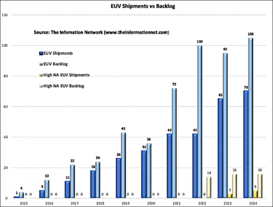
반도체 산업은 고성능, 에너지 효율이 높은 전자기기에 대한 수요로 인해 미세화를 끊임없이 추구하고 있습니다. 극자외선(EUV) 리소그래피, 멀티패터닝, 침지 리소그래피와 같은 첨단 리소그래피 기술은 10나노미터 이하의 미세화를 실현하는 데 매우 중요한 역할을 하며 반도체 제조 능력의 한계를 넓혀가고 있습니다.
세계의 반도체 리소그래피 시장을 종합적으로 분석하고, 시장 규모, 성장 촉진요인, 경쟁 구도, 새로운 시장 기회에 관한 인사이트를 제공하고 있습니다.
목차
제1장 서론
제2장 주요 요약
- 주요 과제 요약
- 시장 기회 요약
제3장 리소그래피의 과제와 동향
- 광학 시스템
- 서론
- 스텝 앤드 리피트 얼라이너
- 심자외선(DUV)
- EUV
- 나노임프린트 리소그래피
- X선 리소그래피
- 전자빔 리소그래피
- 이온 빔 리소그래피
제4장 사용자와 공급업체의 전략
- 리소그래피 요구 결정
- 벤더 벤치마킹
- 가격
- 벤더 커미트먼트와 자세
- 벤더 능력
- 시스템 능력
- 기기 평가중 벤더로부터의 피드백
- 기기 생산중 벤더로부터의 피드백
- 경쟁 환경
- 클래스 1 클린룸용 기기
- 미래의 공장용 기기
- 기회
제5장 시장 예측
- 촉진요인
- 기술 동향
- 경제 동향
- 광학적 한계
- 시장 예측의 전제조건
- 시장 예측
Driving Forces
As semiconductor technology nodes shrink and demand for smaller and more complex semiconductor devices increases, several driving forces push the advancement of lithography technology to meet these challenges:
Technological Scaling: With each new technology node, semiconductor manufacturers aim to reduce the size of transistors and interconnects to improve performance, power efficiency, and density. Advanced lithography techniques are essential for patterning these smaller features with high precision and resolution, driving the development of next-generation lithography tools.
EUV Lithography Adoption: Extreme ultraviolet (EUV) lithography has emerged as a leading candidate for patterning critical layers in advanced semiconductor manufacturing processes. EUV offers shorter wavelengths than traditional optical lithography, enabling the fabrication of smaller feature sizes and more complex patterns. As nodes get smaller, the adoption of EUV lithography becomes increasingly necessary to achieve the required patterning resolution.
Multi-Patterning Techniques: As feature sizes approach the limits of optical lithography, multipatterning techniques such as self-aligned double patterning (SADP), self-aligned quadruple patterning (SAQP), and multi-beam maskless lithography (MBML) become indispensable for achieving the desired feature density and pitch. These techniques involve multiple exposure and etching steps to create intricate patterns, driving the need for advanced lithography solutions.
Resolution Enhancement Technologies (RET): To improve the resolution and fidelity of pattern transfer, lithography tools incorporate resolution enhancement techniques such as optical proximity correction (OPC), phase-shift masks (PSM), and source mask optimization (SMO). These RETs help mitigate the effects of diffraction and other optical limitations, enabling the fabrication of finer features at advanced nodes.
Process Control and Yield Improvement: As feature sizes shrink, maintaining tight process control becomes increasingly challenging. Advanced lithography tools incorporate sophisticated metrology and process control capabilities to ensure uniformity, overlay accuracy, and defect reduction. These capabilities are essential for achieving high yields and manufacturing consistency at advanced nodes.
Emerging Applications and Market Demand: Emerging technologies such as artificial intelligence (AI), 5G connectivity, autonomous vehicles, and IoT devices drive the demand for specialized semiconductor devices with specific performance requirements. Advanced lithography solutions are essential for patterning the complex structures and materials required for these applications, driving innovation in lithography technology.
The Need for This Report
Semiconductor lithography stands as a cornerstone in the realm of semiconductor manufacturing, serving as a pivotal process in the creation of intricate semiconductor devices that power modern electronics. As semiconductor technology advances, lithography techniques evolve in tandem, pushing the boundaries of resolution, precision, and throughput to enable the fabrication of ever-smaller and more complex semiconductor structures. This comprehensive report delves into the multifaceted landscape of semiconductor lithography, exploring key technologies, market trends, industry challenges, and future prospects shaping the semiconductor lithography ecosystem.

The semiconductor industry is witnessing a relentless pursuit of miniaturization, driven by the demand for higher-performance and more energy-efficient electronic devices. As feature sizes shrink to nanoscale dimensions, lithography emerges as a critical enabler, allowing semiconductor manufacturers to pattern intricate circuit designs with unparalleled precision. Advanced lithography techniques such as extreme ultraviolet (EUV) lithography, multiple patterning, and immersion lithography play pivotal roles in achieving sub-10 nanometer feature sizes, pushing the limits of semiconductor manufacturing capabilities.
In addition to technological advancements, the semiconductor lithography market is influenced by a myriad of factors, including market dynamics, regulatory policies, and industry collaborations. This report provides a comprehensive analysis of the global semiconductor lithography market, offering insights into market size, growth drivers, competitive landscape, and emerging opportunities. Through a detailed examination of lithography equipment, materials, and processes, stakeholders gain a deeper understanding of the evolving semiconductor lithography landscape and its impact on the semiconductor industry.
Furthermore, the report explores key challenges and bottlenecks facing semiconductor lithography, ranging from mask complexity and defect reduction to cost constraints and yield optimization. By identifying critical issues and potential solutions, stakeholders can devise strategies to mitigate risks and capitalize on growth opportunities in the semiconductor lithography market.
As semiconductor lithography continues to evolve in response to technological advancements and market demands, stakeholders across the semiconductor ecosystem must stay abreast of the latest developments and trends shaping the industry. This report serves as a valuable resource for semiconductor manufacturers, equipment suppliers, investors, and other industry participants seeking actionable insights into the dynamic landscape of semiconductor lithography. Through comprehensive analysis and strategic recommendations, this report empowers stakeholders to navigate the complex terrain of semiconductor lithography and drive innovation in semiconductor manufacturing.
Report Coverage
This report provides a detailed analysis of the global semiconductor lithography market, including historical data, current market size, and projected growth trends. It may also include market segmentation based on technology, end-user industry, and geographical regions.
It explores the various lithography technologies utilized in semiconductor manufacturing, such as optical lithography, extreme ultraviolet (EUV) lithography, multiple patterning, nanoimprint lithography, and others. This section delves into the principles, advancements, and applications of each technology.
Market Segmentation: Unit and Revenue segments the semiconductor lithography market based on technology types are forecast by:
|
|
The report provides insights into market share of lithography vendors by equipment type including revenue and unit shipments. Market shares by vendor are provided since 1992. The report identifies and analyzes current and emerging trends driving the semiconductor lithography market, such as node migration, China sanctions, and new semiconductor materials, particularly silicon carbide.
Table of Contents
Chapter 1. Introduction
- 1.1. The Need For This Report
Chapter 2. Executive Summary
- 2.1. Summary of Major Issues
- 2.2. Summary of Market Opportunities
Chapter 3. Lithography Issues And Trends
- 3.1. Optical Systems
- 3.1.1. Introduction
- 3.1.2. Step-and-Repeat Aligners
- 3.1.3. Deep Ultraviolet (DUV)
- 3.2. EUV
- 3.5. Nano-Imprint Lithography
- 3.4. X-Ray Lithography
- 3.3. Electron Beam Lithography
- 3.4. Ion Beam Lithography
Chapter 4. User - Supplier Strategies
- 4.1. Determining Lithography Needs
- 4.2. Benchmarking a Vendor
- 4.2.1. Pricing
- 4.2.2. Vendor Commitment and Attitudes
- 4.2.3. Vendor Capabilities
- 4.2.4. System Capabilities
- 4.2.5. Vendor Feedback During Equipment Evaluation
- 4.2.6. Vendor Feedback During Device Production
- 4.3. Competitive Environment
- 4.4. Equipment For Class 1 Cleanrooms
- 4.5. Equipment For the Factory of the Future
- 4.6. Opportunities
Chapter 5. Market Forecast
- 5.1. Driving Forces
- 5.1.1. Technical Trends
- 5.1.2. Economic Trends
- 5.1.3. Optical Limitations
- 5.2. Market Forecast Assumptions
- 5.3. Market Forecast
