|
시장보고서
상품코드
1687765
반도체 에칭 장비 : 시장 점유율 분석, 산업 동향 및 통계, 성장 예측(2025-2030년)Semiconductor Etch Equipment - Market Share Analysis, Industry Trends & Statistics, Growth Forecasts (2025 - 2030) |
||||||
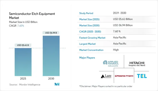
반도체 에칭 장비 시장 규모는 2025년 256억 1,000만 달러, 2030년에는 369억 4,000만 달러에 이를 것으로 예상되며, 예측 기간 중(2025-2030년) CAGR은 7.6%를 나타낼 것으로 전망됩니다.

주요 하이라이트
- 설비투자는 반도체 에칭 장비의 성장을 견인 : 반도체 에칭 장비 시장은 반도체 공정에 대한 설비투자 증가로 강력한 성장을 이루고 있습니다. 미국 기업은 시장을 독점하고 있으며, 주요 제조 공정 범주의 50% 이상을 지배하고 있으며, 일본은 포토레지스트 가공 시장의 90%를 차지하고 있습니다.
- 중국의 투자 : 중국은 2020-2025년 사이에 1조 4,000억 달러를 투자할 계획을 발표하고, 반도체를 포함한 첨단 기술에 주력하고 있습니다.
- 일본의 공동투자 : TSMC와 Sony Corp.은 공동으로 일본의 새로운 칩 공장에 70억 달러를 투자했습니다.
- EU의 디지털 인프라 중점화 : 유럽 연합(EU)은 9,170억 달러의 Covid 부흥 기금의 최대 20%를 마이크로 일렉트로닉스를 중심으로 한 디지털 인프라에 할당했습니다.
- 인텔의 대규모 투자 : 인텔은 독일의 새로운 메가팹을 포함한 유럽 전역에서 880억 달러의 투자 계획을 발표했습니다.
- 기술진보에 의한 시장정세의 재구축 : 급속한 기술진보에 의해 반도체 에칭 장비 시장은 재구축되고 있어 화학약품의 소비량이 적고, 웨이퍼 제조의 자동화에 적합한 플라즈마 에칭 시스템으로의 시프트가 선명해지고 있습니다.
- 선택 에칭 : Lam Research는 2022년 2월, 게이트 올 어라운드(GAA) 트랜지스터 아키텍처용의 혁신적인 웨이퍼 제조 기술을 채용한 선택 에칭 디바이스를 발표했습니다.
- 표면 처리 기술 : ClassOne Technology는 2022년 7월에 표면 처리(SP) 기술을 탑재한 Solstice 자동 매엽식 플랫폼을 확장했습니다.
- 열처리 혁신 : Plasma-Therm은 Heatpulse Rapid Thermal Processing(RTP) 플랫폼을 쇄신하여 세계의 칩 제조업체로부터 복수의 구입을 획득했습니다.
- FPD 장치 개발 : TV, 스마트폰 등의 고해상도화, 초저소비전력화에 대응한 FPD 제조 장치의 개발을 진행하고 있습니다.
- 다용도를 반영한 시장 세분화 : 반도체 에칭 장비 시장은 제품 유형, 에칭막 유형, 용도별로 구분됩니다. 도체 에칭 부문은 2022년부터 2027년까지 연평균 4.55%를 나타내 예측 기간이 끝날 때까지 미화 12,554.46백만 달러에 이를 것으로 예상됩니다.
- 주요 촉진요인 : 주조, MEMS, 센서, 파워 디바이스가 시장 성장을 견인하는 주요 용도 분야입니다.
- 스마트 디바이스와 IoT : IoT의 채용이나 스마트 디바이스 수요 증가에 의해 반도체의 미세화 요구가 높아지고 있어 에칭 장비 시장의 활성화에 연결되고 있습니다.
- 태양전지용 습식 에칭 : 습식 에칭은 그 높은 선택성과 재료 보존 특성에 의해 태양전지 제조에 계속 응용되고 있습니다.
- 투자분석이 밝히는 시장의 가능성 : 반도체 에칭 장비 시장에는 그 성장의 가능성을 반영하여 다액의 투자가 이루어지고 있습니다.
- Lam Research의 확대 : Lam Research는 2021년 8월 말레이시아에 최대 규모의 시설을 개설하여 세계적인 제조 거점을 강화했습니다.
- 미국의 반도체 투자 : 미국 정부는 생산, 연구, 설계에 중점을 둔 반도체 산업에 대한 500억 달러의 투자를 승인했습니다.
- 인도의 반도체 추진 : 인도는 반도체 제조에 100억 달러의 투자를 결정해, 다양한 제조 공장의 설립을 목표로 합니다.
- MIT.nano의 연구개발 확대 : MIT.nano는 2021년 7월, SAMCO의 유도 결합 플라즈마(ICP) 반응성 이온 에칭(RIE) 장치를 새롭게 도입하여 신규 재료의 연구를 강화했습니다.
반도체 에칭 장비 시장 동향
고밀도 에칭 장비 부문이 큰 시장 점유율을 차지
- 압도적인 시장 점유율과 강력한 성장 : 고밀도 에칭 장비 부문이 최대 시장 점유율을 차지하고 2021년 반도체 에칭 장비 시장의 63.59%를 차지했으며, 125억 4,410만 달러에 달했습니다.
- 수요를 견인하는 기술의 진보 : 산업계가 스마트 에브리싱을 추진함에 따라, 보다 소형으로 효율적인 디바이스에 수요가 급증하고 있습니다.
- 첨단 에칭 기술로의 시프트 : 업계는 기존의 습식 에칭에서 보다 효율적이고 매엽 제조의 자동화에 적합한 플라즈마 에칭 시스템으로 크게 이행하고 있습니다.
- 연구개발에 대한 투자 : 반도체 분야에서는 다액의 연구개발투자가 필수적입니다.
업계의 혁신
- ClassOne의 Solstice 확장 : ClassOne Technology는 2022년 7월 새로운 표면 처리 기술을 Solstice 플랫폼에 통합했습니다.
- Plasma-Therm의 RTP 플랫폼 : Plasma-Therm의 주력 제품인 Heatpulse RTP 플랫폼은 최근의 오버홀 후 세계의 주요 칩 제조업체로부터 복수 구입되었습니다.
아시아태평양이 현저한 성장을 이루
- 시장의 리더십과 급성장 : 아시아태평양은 2021년 반도체 에칭 장비 시장에서 84.72%의 점유율을 차지하며, 167억 1,000만 달러의 규모를 기록했습니다.
- 중국의 자립에의 추진 : 중국은 7nm 칩 생산의 자립을 향해 크게 전진해, 몇개의 반도체 제조 분야의 툴이나 노하우를 개발하고 있습니다.
- 전략적 투자와 제휴 : 이 지역은 국내외 선수들로부터 많은 돈을 모으고 있습니다.
- 제조 현지화 : 세계 기업은 아시아태평양에서의 생산을 점점 현지화하고 있습니다.
- 수요를 견인하는 자동차산업 : 완전자율주행차의 개발은 특히 아시아태평양의 반도체산업에 큰 영향을 미칠 것으로 예상됩니다.
반도체 에칭 장비 산업 개요
세계 리더가 연결 시장을 독점 : 반도체 에칭 장비 시장은 세계 기업와 전문 기업에 의해 고도로 통합되고 있습니다.
혁신과 기술력이 시장 리더를 결정 : 시장을 선도하는 주요 기업은 Applied Materials Inc., Lam Research, Tokyo Electron Limited, Hitachi High-Technologies America Inc. 등 기업은 플라즈마 에칭 시스템과 고밀도 유도 결합 플라즈마(ICP) 에칭 기술의 개발에 주력하고 있으며, 지속적인 연구개발에 의해 그 지위를 유지하고 있습니다.
향후 시장 성공을 위한 전략 : 보다 큰 시장 점유율을 획득하기 위해서는 특히 작은 노드 사이즈에 대한 정밀도와 효율의 혁신에 주력할 필요가 있습니다.
기타 혜택
- 엑셀 형식 시장 예측(ME) 시트
- 3개월간의 애널리스트 서포트
목차
제1장 서론
- 조사의 전제조건과 시장 정의
- 조사 범위
제2장 조사 방법
제3장 주요 요약
제4장 시장 인사이트
- 시장 개요
- 업계의 매력도 - Porter's Five Forces 분석
- 공급기업의 협상력
- 구매자의 협상력
- 신규 참가업체의 위협
- 대체품의 위협
- 경쟁 기업간 경쟁 관계의 강도
- 시장에 대한 COVID-19의 영향 평가
제5장 시장 역학
- 시장 성장 촉진요인
- 반도체 공정에 대한 설비 투자 증가
- 급속한 기술의 진보와 이행
- 시장 성장 억제요인
- 무역 불안과 반도체 메모리 시장
제6장 시장 세분화
- 제품 유형별
- 고밀도 에칭 장비
- 저밀도 에칭 장비
- 에칭 필름 유형별
- 도체 에칭
- 유전체 에칭
- 폴리 실리콘 에칭
- 용도별
- 파운드리
- MEMS
- 센서
- 전력 장치
- 지역별
- 북미
- 유럽
- 아시아
- 호주 및 뉴질랜드
- 라틴아메리카
- 중동 및 아프리카
제7장 경쟁 구도
- 기업 프로파일
- Applied Materials Inc.
- Hitachi High Technologies America, Inc.
- Lam Research Corporation
- Tokyo Electron Limited
- Plasma-Therm LLC
- Panasonic Corporation
- SPTS Technologies Limited(Orbotech)
- Suzhou Delphi Laser Co., Ltd
- ULVAC Inc.
제8장 투자 분석
제9장 시장 기회와 앞으로의 동향
KTH 25.05.09The Semiconductor Etch Equipment Market size is estimated at USD 25.61 billion in 2025, and is expected to reach USD 36.94 billion by 2030, at a CAGR of 7.6% during the forecast period (2025-2030).
Key Highlights
- Capital Spending Drives Semiconductor Etch Equipment Growth: The Semiconductor Etch Equipment Market is experiencing robust growth, fueled by increased capital spending on semiconductor processing. Global investments in the semiconductor industry have surged, with countries like France allocating USD 1.9 billion and Germany investing USD 12 billion into microelectronics projects. US firms dominate the market, controlling over 50% of major manufacturing process equipment categories, while Japan commands 90% of the photoresist processing market. This investment surge is propelling demand for advanced etching technologies, critical for producing smaller, thinner, and faster devices.
- China's Investment: China announced plans to invest USD 1.4 trillion between 2020 and 2025, focusing on advanced technologies, including semiconductors.
- Joint Investment in Japan: TSMC and Sony Corp. jointly invested USD 7 billion in a new chip factory in Japan.
- EU's Digital Infrastructure Focus: The European Union allocated up to 20% of its USD 917 billion Covid recovery fund toward digital infrastructure, focusing on microelectronics.
- Intel's Mega Investment: Intel unveiled plans for a USD 88 billion investment across Europe, including a new "megafab" in Germany.
- Technological Advancements Reshape Market Landscape: Rapid technological advancements are reshaping the Semiconductor Etch Equipment Market, with a clear shift towards plasma etch systems, which consume fewer chemicals and are more suited for automating single wafer manufacturing. This evolution is driven by the growing demand for energy-efficient electronic devices with improved performance, spurring the development of miniature semiconductor integrated circuits (ICs).
- Selective Etching: Lam Research introduced selective etch devices in February 2022, employing innovative wafer fabrication techniques for gate-all-around (GAA) transistor architectures.
- Surface Preparation Tech: ClassOne Technology expanded its Solstice automated single-wafer platform with surface preparation (SP) technologies in July 2022.
- Thermal Processing Innovation: Plasma-Therm revamped its Heatpulse Rapid Thermal Processing (RTP) platform, securing multiple purchases from global chipmakers.
- FPD Equipment Development: Tokyo Electron continues to evolve its FPD production equipment, optimizing it for higher resolutions and ultra-low power consumption for TVs, smartphones, and other devices.
- Market Segmentation Reflects Diverse Applications: The Semiconductor Etch Equipment Market is segmented by product type, etching film type, and application. High-density etch equipment leads the market, with revenue expected to reach USD 19,289.61 million by 2027. The conductor etching segment is forecasted to grow at a CAGR of 4.55% from 2022 to 2027, reaching USD 12,554.46 million by the end of the forecast period.
- Key Growth Drivers: Foundries, MEMS, sensors, and power devices are key application areas driving market growth.
- Smart Devices and IoT: The adoption of IoT and growing demand for smart devices are increasing the need for miniature semiconductors, fueling the etch equipment market.
- Wet Etching for Solar Cells: Wet etching continues to find applications in solar cell manufacturing due to its high selectivity and material preservation properties.
- Investment Analysis Reveals Market Potential: Significant investments are pouring into the Semiconductor Etch Equipment Market, reflecting its potential for growth. Companies are scaling up manufacturing capacities and boosting R&D efforts to meet the rising demand for advanced semiconductor technologies.
- Lam Research's Expansion: Lam Research Corporation opened its largest facility in Malaysia in August 2021, enhancing its global manufacturing footprint.
- US Semiconductor Investment: The US government approved a USD 50 billion investment in the semiconductor industry, focusing on production, research, and design.
- India's Semiconductor Push: India greenlit a USD 10 billion investment in semiconductor manufacturing, aiming to establish a variety of fabrication plants.
- MIT.nano's R&D Expansion: MIT.nano acquired a new SAMCO inductively coupled plasma (ICP) reactive-ion etching (RIE) system in July 2021, boosting research into novel materials.
Semiconductor Etch Equipment Market Trends
High-Density Etch Equipment Segment Holds Significant Market Share
- Dominant Market Share and Robust Growth: The high-density etch equipment segment holds the largest market share, comprising 63.59% of the semiconductor etch equipment market in 2021, valued at USD 12,544.1 million. Projections indicate that this segment will grow to USD 19,289.6 million by 2027, at a compound annual growth rate (CAGR) of 5.66%.
- Technological Advancements Driving Demand: As industries push for "smart everything," demand for smaller, more efficient devices is soaring. This trend is propelling semiconductor manufacturing technologies to deliver precision in high-temperature chemical processes, where cleanliness and precise chemical dosing are key.
- Shift to Advanced Etching Technologies: The industry has largely transitioned from traditional wet etching to plasma etch systems, which are more efficient and better suited for automating single wafer manufacturing. This shift is essential for the development of miniature semiconductor ICs, which power energy-efficient devices.
- Investment in Research and Development: Heavy R&D investment is critical in the semiconductor sector. The United States, for instance, has committed to doubling research investments in semiconductor-related fields, aiming to spur innovation in artificial intelligence, quantum computing, and advanced wireless technologies.
Industry Innovations:
- ClassOne's Solstice Expansion: ClassOne Technology incorporated new surface preparation technologies into its Solstice platform in July 2022.
- Plasma-Therm's RTP Platform: Plasma-Therm's flagship Heatpulse RTP platform saw multiple purchases from major global chipmakers after its recent overhaul.
Asia-Pacific to Witness Significant Growth
- Market Leadership and Rapid Growth: Asia Pacific dominates the semiconductor etch equipment market with an 84.72% market share in 2021, valued at USD 16.71 billion. This region is projected to grow at a CAGR of 4.52%, reaching USD 23.80 billion by 2029.
- China's Push for Self-Reliance: China has made substantial progress towards self-reliance in 7nm chip production, developing tools and know-how for several semiconductor manufacturing segments. This drive for self-sufficiency is a major factor propelling investments and innovations in semiconductor etch equipment in the region.
- Strategic Investments and Collaborations: The region has attracted significant investment from both domestic and international players. For example, TSMC announced a USD 2.8 billion investment in China to ramp up automotive chip production. Similarly, India is making strides with ISMC's planned USD 3 billion semiconductor manufacturing facility.
- Localization of Manufacturing: Global companies are increasingly localizing production in Asia Pacific. In February 2022, Lam Research started manufacturing next-generation core equipment in South Korea, strengthening its ties with Samsung Electronics' memory and system semiconductor production.
- Automotive Industry Driving Demand: The development of fully-autonomous vehicles is expected to significantly impact the semiconductor industry, particularly in Asia Pacific. As the automotive and semiconductor industries work to enhance technologies for autonomous driving, demand for semiconductor and etch equipment is expected to rise sharply.
Semiconductor Etch Equipment Industry Overview
Global Leaders Dominate Consolidated Market: The Semiconductor Etch Equipment Market is highly consolidated, dominated by global players and specialized companies. The largest players hold significant market shares, owing to the high barriers to entry in terms of capital and technological expertise. Large, multinational corporations with extensive research capabilities primarily drive the market.
Innovation and Technological Prowess Define Market Leaders: Key market leaders include Applied Materials Inc., Lam Research Corporation, Tokyo Electron Limited, and Hitachi High-Technologies America Inc. These companies maintain their positions through continuous R&D, focusing on advancing plasma etch systems and high-density inductively coupled plasma (ICP) etching technologies. Their global reach and strategic partnerships with key semiconductor manufacturers further solidify their market dominance.
Strategies for Future Success in the Market: To gain a larger market share, players must focus on innovation in precision and efficiency, particularly for smaller node sizes. Expanding manufacturing capacity and forming strategic partnerships with research institutions and semiconductor manufacturers will also be key. Moreover, adapting to the growing demand for semiconductors driven by trends like IoT and AI will be essential for success in this competitive market.
Additional Benefits:
- The market estimate (ME) sheet in Excel format
- 3 months of analyst support
TABLE OF CONTENTS
1 INTRODUCTION
- 1.1 Study Assumptions and Market Definition
- 1.2 Scope of the Study
2 RESEARCH METHODOLOGY
3 EXECUTIVE SUMMARY
4 MARKET INSIGHTS
- 4.1 Market Overview
- 4.2 Industry Attractiveness - Porter's Five Forces Analysis
- 4.2.1 Bargaining Power of Suppliers
- 4.2.2 Bargaining Power of Buyers
- 4.2.3 Threat of New Entrants
- 4.2.4 Threat of Substitute Products
- 4.2.5 Intensity of Competitive Rivalry
- 4.3 Assessment of the Impact of COVID-19 on the Market
5 MARKET DYNAMICS
- 5.1 Market Drivers
- 5.1.1 Increase in Capital Spending on Semiconductor Processing
- 5.1.2 Rapid Technological Advances and Transition
- 5.2 Market Restraints
- 5.2.1 Trade Uncertainties and Semiconductor Memory Markets
6 MARKET SEGMENTATION
- 6.1 By Product Type
- 6.1.1 High-density Etch Equipment
- 6.1.2 Low-density Etch Equipment
- 6.2 By Etching Film Type
- 6.2.1 Conductor Etching
- 6.2.2 Dielectric Etching
- 6.2.3 Polysilicon Etching
- 6.3 By Application
- 6.3.1 Foundries
- 6.3.2 MEMS
- 6.3.3 Sensors
- 6.3.4 Power Devices
- 6.4 By Geography
- 6.4.1 North America
- 6.4.2 Europe
- 6.4.3 Asia
- 6.4.4 Australia and New Zealand
- 6.4.5 Latin America
- 6.4.6 Middle East and Africa
7 COMPETITIVE LANDSCAPE
- 7.1 Company Profiles
- 7.1.1 Applied Materials Inc.
- 7.1.2 Hitachi High Technologies America, Inc.
- 7.1.3 Lam Research Corporation
- 7.1.4 Tokyo Electron Limited
- 7.1.5 Plasma-Therm LLC
- 7.1.6 Panasonic Corporation
- 7.1.7 SPTS Technologies Limited (Orbotech)
- 7.1.8 Suzhou Delphi Laser Co., Ltd
- 7.1.9 ULVAC Inc.