
|
시장보고서
상품코드
2035097
패널 레벨 패키징 시장 : 점유율 분석, 산업 동향 및 통계 데이터, 성장 예측(2026-2031년)Panel Level Packaging - Market Share Analysis, Industry Trends & Statistics, Growth Forecasts (2026 - 2031) |
||||||
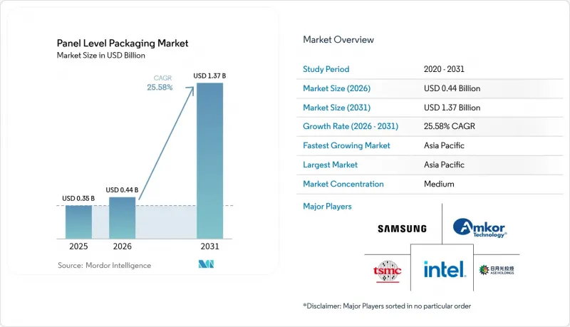
패널 레벨 패키징 시장 규모는 2025년 3억 5,000만 달러에서 2026년에는 4억 4,000만 달러로 확대되어 2026년부터 2031년까지 CAGR 25.58%로 성장을 지속하여, 2031년까지 13억 7,000만 달러에 이를 것으로 예측됩니다.

이러한 급격한 성장 궤적은 반도체 산업이 웨이퍼 중심 아키텍처에서 패널 중심 아키텍처로 전환하고 있으며, 이러한 움직임은 AI 및 고성능 컴퓨팅의 급증하는 수요에 대응할 수 있는 규모의 경제를 가져다 줄 것입니다. 패널 형식은 멀티 다이 설계에서 최대 40% 더 높은 기판 활용도를 실현하고, 로직 및 메모리 노드가 5nm 이하로 미세화됨에 따라 비용 압박을 완화할 수 있습니다. 기판 혁신, 특히 유리 코어로의 전환은 보다 엄격한 치수 제어와 열 안정성 향상을 약속하고 있으며, 이는 증가하는 입출력 수에 대응할 수 있도록 지원하고 있습니다. 장비 벤더들은 10µm 이하의 미세구조를 구현할 수 있는 600 mmX600 mm 리소그래피 시스템으로 이에 대응하고 있으며, 기존 해상도의 한계를 극복하고 차세대 집적화를 위한 대상 시장을 확대되고 있습니다. 주요 파운더의 수직 통합 전략과 파운더와 OSAT 파트너 간의 협력적 생산 능력 확대에서 볼 수 있듯이, 공급망 연계가 강화되고 있습니다.
세계 패널 레벨 패키징 시장 동향 및 인사이트
비용 절감과 웨이퍼 레벨 패키징의 비교
패널 형태로의 전환은 멀티 다이 설계에서 기판 활용도를 최대 40%까지 향상시켜 고가의 금형 비용을 감안하더라도 실장 당 비용을 절감할 수 있습니다. ASE의 310mmX310mm 라인에 대한 2억 달러 투자는 양산 확대에 대한 약속을 보여주며, 대량 생산되는 소비자 디바이스가 짧은 수명주기 동안 금형 비용을 상각하는 데 필요한 웨이퍼 시작 횟수를 공급하고 있습니다. 아시아 위탁생산 업체들은 기판 제조, 재배선층(RDL) 처리, 최종 테스트를 단일 캠퍼스 내에 통합함으로써 물류 비용을 절감하고, 추가적인 이점을 얻고 있습니다. 생산량이 적은 유럽과 미국 제조업체는 비용 곡선이 가파르게 상승하여 경쟁 격차가 확대되고 있습니다. 그 결과, 턴키 패키지 입찰에서 패널 우선 전략이 수주율을 결정짓는 경우가 늘고 있습니다.
AI/HPC 칩 수요 급증
대규모 언어 모델 추론 및 훈련 환경은 그 어느 때보다 고밀도 GPU 클러스터가 필요하며, 대역폭을 유지할 수 있는 인터포저를 사용하지 않는 대형 패키지로의 전환을 촉진하고 있습니다. TSMC의 'CoPoS(Chip on Panel on Board(CoPoS)' 로드맵은 2027년 리스크 생산 시작을 계획하고 있으며, 열 저항을 일정하게 유지하면서 CoWoS의 레티클 제한 치수를 두 배로 확대할 예정입니다. 파운드리는 2026년까지 연간 60% 이상의 속도로 CoWoS 생산 능력을 확장하고 있지만, 여전히 고대역폭 메모리(HBM) 라인의 주문 잔량이 예상되며, Tier 1 고객들은 차세대 가속기 카드를 위한 패널 레벨 패키징 시장의 대안을 고려해야 하는 상황입니다. 패널 패키지에서 20kW 이상의 선반 레벨 냉각을 입증할 수 있는 선도 기업이 다년간공급 계약을 체결할 수 있는 가장 유리한 위치에 있습니다.
높은 설비투자 비용과 뒤틀림 문제
600mm 라인을 풀가동하려면 성막, 패터닝, 계측 장비에 5억 달러 이상이 필요합니다. 패널 기판은 열 하중을 받으면 팽창하고, 보정하지 않으면 2mm 이상의 휨이 발생합니다. SK Key 파운데이션과 LB세미콘의 Direct-RDL 플로우에서는 경화 시 패널의 끝부분을 고정하여 휨을 억제하고 있지만, 장비 개조로 인해 공구비용이 15% 증가합니다. 소규모 OSAT(위탁 반도체 조립업체)는 이러한 업그레이드를 위한 자금 조달에 어려움을 겪고 있으며, 이는 전 세계 공급 확대에 걸림돌이 되고 있습니다. 저탄성 유전체나 능동형 휨 보정 척이 실용화되기 전까지는 수율 저하가 패널 레벨 패키징 시장으로의 단기적인 침투를 가로막는 요인으로 작용할 것입니다.
부문 분석
팬아웃 패널 레벨 패키징은 2025년 매출의 44.60%를 차지했으며, 적당한 I/O 밀도로 충분한 민수용 및 모바일 기기용 주력 제품입니다. 이 부문의 패널 레벨 패키징 시장 규모는 1억 6,000만 달러에 달하며 2031년까지 연평균 19.80%의 성장률을 보일 것으로 예측됩니다. 주요 OSAT(위탁 반도체 제조업체)는 성숙한 DFD(Die Face Down) 공정을 활용하여 수율을 97% 이상 향상시켰으며, 월2만장 이상의 생산량에서 웨이퍼 팬아웃 방식의 비용을 두 자릿수 차이로 낮추고 있습니다. 그러나 대역폭을 많이 소비하는 액셀러레이터는 이 방식의 패드 피치 한계에 다다랐고, 혁신가들은 2.5D/3D 패널 솔루션으로 이동하고 있습니다.
2.5D/3D 패널 통합은 2025년 매출에서 차지하는 비중은 19.10%에 불과했지만, CAGR 29.20%로 가장 빠르게 성장하고 있습니다. 이기종 스태킹(heterogeneous stacking)을 통해 연산, 메모리, 아날로그 타일을 패시브 유리 캐리어에 배치하여 상호 연결 길이를 최대 70%까지 줄일 수 있습니다. 초기 상용화 사례는 단일 패키지에 16개 이상의 칩렛을 탑재한 AI 추론 카드가 주를 이루고 있습니다. 2.5D/3D 접근 방식의 패널 레벨 패키징 시장 점유율은 2031년까지 31.80%를 나타낼 것으로 예측되며, 이 기술이 데이터센터의 틈새 시장을 벗어나 자동차 도메인 컨트롤러에도 적용될 것으로 전망됩니다.
유기 라미네이트는 저비용 수지 시스템과 확립 된 공급망의 혜택을 받아 2025 년에는 56.10%의 점유율을 유지하여 시장 규모가 2억 달러에 달했습니다. 그러나 이 부문의 CAGR은 20.40%에 불과해 전체 패널 레벨 패키징 시장보다 낮았습니다. 이는 적층 수의 물리적 한계와 열팽창계수(CTE)의 불일치를 반영합니다. 반면, 유리 코어는 지난해 12.30%의 점유율에 불과했지만, 2031년까지 연평균 복합 성장률(CAGR) 28.90%를 나타낼 것으로 예측됩니다. 삼성의 H-glass 로드맵은 2026년 양산을 목표로 하고 있으며, 0.3 ppm/°C의 치수 드리프트(유기 재료의 10분의 1)를 실현하고, 5µm 미만의 선폭을 가진 리배선 층을 가능하게 합니다. 실리콘 및 성형 재구성 패널은 여전히 틈새 시장으로 고출력 또는 초저가 분야에 제공되고 있습니다.
지역별 분석
아시아태평양은 2025년 매출의 69.20%를 차지했고 2031년까지 연평균 27.60%의 연평균 복합 성장률(CAGR)로 패널 레벨 패키징 시장을 주도할 것으로 예측됩니다. 중국은 국가 AI 칩 프로그램에 따라 패널 패키징 라인에 대한 정부 인센티브를 제공하고 있으며, 일본의 설비 투자 금액은 2024년 82% 증가하여 70억 달러에 달했으며, 국내 공정 능력을 뒷받침하고 있습니다. 한국은 유리 코어 기판 개발을 진행하고 있으며, 대만의 TSMC는 CoWoS, CoPoS 및 테스트를 단일 팹 클러스터에 통합한 파운드리-패키징 통합 플로우를 추진하고 있습니다.
북미도 이에 이어 첨단 패키징을 위해 할당된 CHIPS 법에 따라 16억 달러의 자금을 축으로 삼고 있습니다. 4억 달러 규모의 AMCOL의 애리조나 공장은 2026년에 가동될 예정이며, TSMC의 새로운 Fab 21과 같은 부지에 위치하여 미국 고객사의 사이클 타임을 단축할 수 있습니다. SK 하이닉스도 마찬가지로 인디애나주에서 HBM 패키징에 4억 5,000만 달러를 배정하는 등 각 주정부가 고부가가치 백엔드 사업을 적극적으로 유치하고 있음을 알 수 있습니다.
유럽의 점유율은 여전히 한 자릿수에 머물러 있지만, 자국 생산에 대한 우려로 현지 OSAT(반도체 위탁생산) 기업 설립이 진행되어 점유율이 상승하는 추세입니다. 폭스콘과 탈레스는 항공우주 및 방위 분야를 위한 새로운 팬아웃 시설에 2억 5,000만 유로를 투자하기로 결정했습니다. 한편, 인피니언은 Amkor와 협력하여 2025년 중반에 가동될 예정인 포르투갈의 패널 생산능력 증설을 추진했습니다. 중동, 아프리카 및 남미는 여전히 소비 주도형이며, 현재로서는 조립 거점이 제한적이지만, 사우디아라비아 및 브라질의 인센티브 제도로 인해 10년 후반기에는 그 균형이 바뀔 수 있습니다.
기타 특전:
- 엑셀 형식 시장 예측(ME) 시트
- 3개월간 애널리스트 지원
자주 묻는 질문
목차
제1장 서론
제2장 분석 방법
제3장 주요 요약
제4장 시장 구도
제5장 시장 규모와 성장 예측
제6장 경쟁 구도
제7장 시장 기회와 향후 전망
JHS 26.05.20The panel-level packaging market size is expected to grow from USD 0.35 billion in 2025 to USD 0.44 billion in 2026 and is forecast to reach USD 1.37 billion by 2031 at 25.58% CAGR over 2026-2031.
The steep trajectory mirrors the semiconductor sector's shift from wafer-centric to panel-centric architectures, a move that unlocks scale advantages and aligns with burgeoning AI and high-performance computing demand. Panel formats deliver up to 40% better substrate utilization for multi-die designs, easing cost pressure as logic and memory nodes scale below 5 nm. Substrate innovation, notably the transition toward glass cores, promises tighter dimensional control and improved thermal stability, which together support rising input/output counts. Equipment vendors have responded with 600 mm X 600 mm lithography systems capable of sub-10 µm features, erasing a former resolution ceiling and widening the addressable market for next-generation integration. Supply-chain coordination is intensifying, illustrated by vertically integrated strategies from leading foundries and by cooperative capacity expansions between foundry and OSAT partners.
Global Panel Level Packaging Market Trends and Insights
Cost Reduction Versus Wafer-Level Packaging
Moving to panel formats yields up to 40% better substrate utilization for multi-die designs, cutting cost per placement even after accounting for expensive tooling. ASE's USD 200 million investment in 310 mm X 310 mm lines signals a commitment to volume scaling, and high-volume consumer devices supply the wafer starts needed to amortize tools across short life cycles. Asian contract manufacturers gain further leverage by clustering substrate fabrication, redistribution-layer processing, and final test inside single campuses, reducing logistics overhead. Western houses with lower volumes face a steeper cost curve, widening the competitiveness gap. As a result, panel-first strategies increasingly determine win rates in turnkey package bids.
Surge of AI/HPC Chip Demand
Large language-model inference and training floors require ever-denser GPU clusters, driving packaging toward larger interposer-free footprints that sustain bandwidth. TSMC's Chip-on-Panel-on-Substrate (CoPoS) roadmap, slated for 2027 risk production, doubles reticle-limited dimensions of CoWoS while holding thermal resistance steady. The foundry is expanding CoWoS capacity more than 60% annually through 2026, yet still projects backlog in high-bandwidth memory (HBM) lines, pushing Tier-1 customers to evaluate panel-level packaging market alternatives for next-generation accelerator cards. Early movers able to demonstrate >20 kW shelf-level cooling in panel packages are best positioned to secure multi-year supply agreements.
High Capital Intensity and Warpage Issues
A full 600 mm line demands more than USD 500 million in deposition, patterning, and metrology gear. Panel substrates expand under thermal load, generating a bow that can exceed 2 mm if not compensated. SK Key Foundry and LB Semicon's Direct-RDL flow clamps panel edges during cure to limit deflection, but equipment retrofits add 15% to tool cost. Smaller OSATs struggle to finance those upgrades, constraining global supply expansion. Until low-modulus dielectrics or active warp-compensation chucks mature, yield drag remains a check on near-term penetration of the panel-level packaging market.
Other drivers and restraints analyzed in the detailed report include:
- Proliferation of 5G/6G and Edge Devices
- Nikon 600 X 600 mm digital lithography adoption
- Process-Integration Complexity Beyond 300 mm
For complete list of drivers and restraints, kindly check the Table Of Contents.
Segment Analysis
Fan-Out Panel Level Packaging commanded 44.60% of 2025 revenue, making it the workhorse for consumer and mobile devices where moderate I/O density is sufficient. The panel-level packaging market size for this segment reached USD 0.16 billion and is projected to grow at 19.80% through 2031. Large OSATs leverage mature die-face-down flows to drive yields above 97%, beating wafer fan-out costs by double-digit margins on runs above 20,000 panels per month. Nevertheless, bandwidth-hungry accelerators are stretching the approach's pad pitch limits, pressing innovators toward 2.5D/3D panel solutions.
2.5D/3D panel integration, while holding only 19.10% of 2025 sales, is the fastest mover at a 29.20% CAGR. Heterogeneous stacking places compute, memory, and analog tiles on passive glass carriers, cutting interconnect length by up to 70%. Early commercial wins center on AI inference cards where a single package hosts >16 chiplets. The panel-level packaging market share for 2.5D/3D approaches is expected to hit 31.80% by 2031 as the technique escapes datacenter niches and filters into automotive domain controllers.
Organic laminate retained a 56.10% share in 2025, valued at USD 0.20 billion, benefiting from low-cost resin systems and entrenched supply chains. However, the segment's 20.40% CAGR lags the overall panel-level packaging market, reflecting physical limits on layer count and CTE mismatch. Glass cores, in contrast, posted only an 12.30% share last year but will grow at a 28.90% CAGR to 2031. Samsung's H-glass roadmap targets volume ramp in 2026, offering 0.3 ppm/°C dimensional drift, one-tenth that of organics, unlocking sub-5 µm line-width redistribution layers. Silicon and molded reconstituted panels remain niche, serving high-power or ultra-low-cost corners.
The Panel Level Packaging Market Report is Segmented by Packaging Technology (Fan-Out Panel Level Packaging, Embedded Bridge, and More), Substrate Material (Organic Laminate, Glass Core, and More), Panel Size (<=300mmX300mm, 301-510mmX510mm, >=511mmX600mm), Industry Application (Consumer Electronics, Automotive, and More), and Geography (North America, Europe, and More). The Market Forecasts are Provided in Terms of Value (USD).
Geography Analysis
Asia-Pacific captured 69.20% of 2025 revenue and continues to lead the panel-level packaging market at a 27.60% CAGR through 2031. China funnels state incentives toward panel packaging lines aligned with sovereign AI chip programs, and Japan's equipment outlays rose 82% in 2024 to USD 7 billion, underpinning domestic process capability. South Korea advances glass-core substrates, while Taiwan's TSMC pushes integrated foundry-packaging flows that bundle CoWoS, CoPoS, and testing in a single fab cluster.
North America follows, anchored by CHIPS-Act funding of USD 1.6 billion earmarked for advanced packaging. Amkor's USD 400 million Arizona plant comes online in 2026, co-located with TSMC's new Fab 21 to shorten cycle times for U.S. customers. SK Hynix likewise has earmarked USD 450 million for HBM packaging in Indiana, demonstrating that states are bidding aggressively for high-value backend operations.
Europe's share remains single-digit but is rising as sovereignty concerns spur local OSAT formation. Foxconn and Thales committed EUR 250 million to a new fan-out facility aimed at aerospace and defense, while Infineon partnered with Amkor to add panel capacity in Portugal that comes online mid-2025. Middle East and Africa and South America remain consumption-centric, with limited assembly footprints yet, though incentive schemes in Saudi Arabia and Brazil could shift that balance later in the decade.
- Samsung Electronics Co., Ltd.
- Taiwan Semiconductor Manufacturing Company Limited (TSMC)
- Intel Corporation
- ASE Technology Holding Co., Ltd.
- Amkor Technology, Inc.
- Powertech Technology Inc.
- Nepes Corporation
- Unimicron Technology Corp.
- DECA Technologies, Inc.
- JCET Group Co., Ltd.
- Fraunhofer Institute for Reliability and Microintegration IZM
- Nikon Corporation
- Ajinomoto Fine-Techno Co., Inc.
- Shinko Electric Industries Co., Ltd.
- LG Innotek Co., Ltd.
- K&S (Kulicke & Soffa Industries, Inc.)
- Veeco Instruments Inc.
- Applied Materials, Inc.
- Ultratech (Veeco)
- Tokyo Electron Limited
- Brewer Science, Inc.
Additional Benefits:
- The market estimate (ME) sheet in Excel format
- 3 months of analyst support
TABLE OF CONTENTS
1 Introduction
- 1.1 Study Assumptions and Market Definition
- 1.2 Scope of the Study
2 Research Methodology
3 Executive Summary
4 Market Landscape
- 4.1 Market Overview
- 4.2 Market Drivers
- 4.2.1 Cost reduction versus wafer-level packaging
- 4.2.2 Surge of AI/HPC chip demand
- 4.2.3 Proliferation of 5G/6G and edge devices
- 4.2.4 Nikon 600 x 600 mm digital lithography adoption
- 4.2.5 Shift to glass-core substrates >=2026
- 4.2.6 EU/US reshoring subsidies tied to advanced packaging
- 4.3 Market Restraints
- 4.3.1 High capital intensity and warpage issues
- 4.3.2 Process-integration complexity beyond 300 mm
- 4.3.3 Sub-1 µm lithography yield cliff on large panels
- 4.3.4 Supply bottleneck for ABF-GCP dielectric films
- 4.4 Industry Value Chain Analysis
- 4.5 Regulatory Landscape
- 4.6 Technological Outlook
- 4.7 Porter's Five Forces Analysis
- 4.7.1 Bargaining Power of Suppliers
- 4.7.2 Bargaining Power of Buyers
- 4.7.3 Threat of New Entrants
- 4.7.4 Threat of Substitutes
- 4.7.5 Intensity of Rivalry
5 Market Size and Growth Forecasts (Value)
- 5.1 By Packaging Technology
- 5.1.1 Fan-Out Panel Level Packaging (FOPLP)
- 5.1.2 Embedded Bridge (eBridge)
- 5.1.3 2.5D/3D Panel Integration
- 5.1.4 Fan-In Panel Level Packaging
- 5.2 By Substrate Material
- 5.2.1 Organic Laminate
- 5.2.2 Glass Core
- 5.2.3 Silicon
- 5.2.4 Molded Reconstituted Panel
- 5.3 By Panel Size
- 5.3.1 <=300 mm X 300 mm
- 5.3.2 301 - 510 mm X 510 mm
- 5.3.3 >=511 mm X 600 mm
- 5.4 By Industry Application
- 5.4.1 Consumer Electronics
- 5.4.2 Automotive (ADAS, EV Power)
- 5.4.3 Telecommunications (5G/6G Infrastructure)
- 5.4.4 Aerospace and Defense
- 5.4.5 Industrial and IoT
- 5.5 By Geography
- 5.5.1 North America
- 5.5.1.1 United States
- 5.5.1.2 Canada
- 5.5.1.3 Mexico
- 5.5.2 South America
- 5.5.2.1 Brazil
- 5.5.2.2 Argentina
- 5.5.2.3 Rest of South America
- 5.5.3 Europe
- 5.5.3.1 Germany
- 5.5.3.2 United Kingdom
- 5.5.3.3 France
- 5.5.3.4 Italy
- 5.5.3.5 Rest of Europe
- 5.5.4 Asia-Pacific
- 5.5.4.1 China
- 5.5.4.2 Japan
- 5.5.4.3 South Korea
- 5.5.4.4 India
- 5.5.4.5 Rest of Asia-Pacific
- 5.5.5 Middle East
- 5.5.5.1 Saudi Arabia
- 5.5.5.2 United Arab Emirates
- 5.5.5.3 Rest of Middle East
- 5.5.6 Africa
- 5.5.6.1 South Africa
- 5.5.6.2 Rest of Africa
- 5.5.1 North America
6 Competitive Landscape
- 6.1 Market Concentration
- 6.2 Strategic Moves
- 6.3 Market Share Analysis
- 6.4 Company Profiles (includes Global level Overview, Market level overview, Core Segments, Financials as available, Strategic Information, Market Rank/Share for key companies, Products and Services, and Recent Developments)
- 6.4.1 Samsung Electronics Co., Ltd.
- 6.4.2 Taiwan Semiconductor Manufacturing Company Limited (TSMC)
- 6.4.3 Intel Corporation
- 6.4.4 ASE Technology Holding Co., Ltd.
- 6.4.5 Amkor Technology, Inc.
- 6.4.6 Powertech Technology Inc.
- 6.4.7 Nepes Corporation
- 6.4.8 Unimicron Technology Corp.
- 6.4.9 DECA Technologies, Inc.
- 6.4.10 JCET Group Co., Ltd.
- 6.4.11 Fraunhofer Institute for Reliability and Microintegration IZM
- 6.4.12 Nikon Corporation
- 6.4.13 Ajinomoto Fine-Techno Co., Inc.
- 6.4.14 Shinko Electric Industries Co., Ltd.
- 6.4.15 LG Innotek Co., Ltd.
- 6.4.16 K&S (Kulicke & Soffa Industries, Inc.)
- 6.4.17 Veeco Instruments Inc.
- 6.4.18 Applied Materials, Inc.
- 6.4.19 Ultratech (Veeco)
- 6.4.20 Tokyo Electron Limited
- 6.4.21 Brewer Science, Inc.
7 Market Opportunities and Future Outlook
- 7.1 White-space and Unmet-need Assessment
