
|
시장보고서
상품코드
1630292
임베디드 다이 패키징 : 시장 점유율 분석, 산업 동향 및 통계, 성장 예측(2025-2030년)Embedded Die Packaging - Market Share Analysis, Industry Trends & Statistics, Growth Forecasts (2025 - 2030) |
||||||
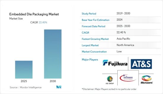
임베디드 다이 패키징 시장은 예측 기간 동안 22.4%의 CAGR을 기록할 것으로 예상됩니다.
주요 하이라이트
- 제품의 소형화 및 다기능화, 기기 소형화가 시장 주도 마이크로 가공 및 나노기술은 생물 의학 응용에서 화학 마이크로 반응기 및 센서에 이르기까지 부품의 소형화에 점점 더 중요한 역할을 하고 있습니다. 예를 들어, 블루투스 무선랜 모듈은 오늘날의 고밀도 휴대용 기기에서 최소한의 회로 기판 면적을 필요로 합니다.
- 전기적 및 열적 성능의 개선이 시장을 주도하고 있습니다. 전력 관리 및 모바일 무선 애플리케이션에서 임베디드 기술은 더 얇은 두께와 우수한 열 성능으로 인해 어셈블리 제조를 대체할 수 있는 것으로 평가받고 있습니다. 임베디드 다이의 열 성능은 구리 클립을 사용하는 PQFN보다 약 17% 더 우수합니다. 또한, 전기자동차를 위해 임베디드 다이와 리와이어링 레이어(RDL) 기술을 사용하여 전기적 성능과 열적 성능을 향상시키는 새로운 확장 가능한 전력 장치용 첨단 패키징을 개발했습니다.
- 또한, 고주파에서 우수한 전기적 성능으로 인해 이 기술은 신흥 IT 및 통신 응용 분야에서 유망한 기술로 인정받고 있습니다. 이 기술을 통신 애플리케이션에 적용하는 데 도움이 되는 다양한 이점으로는 전자 회로의 기능 및 효율성 향상, 전력 및 신호 인덕턴스, 신뢰성 향상, 신호 밀도 향상 등이 있습니다.
- 테스트, 검사 및 수정이 어려운 임베디드 다이 기술은 시장 성장의 과제입니다. 피처(라인 또는 공간)가 2μm 이하로 미세화되면 결함을 보기가 어려워집니다. 또한, 애플리케이션에 따라서는 비아홀 내 이물질 발견이 우려되는 경우도 있습니다.
- COVID-19가 발생한 이후 전자 산업은 큰 타격을 입어 공급망과 생산 설비에 큰 영향을 미쳤으며, 2월부터 3월까지 중국과 대만에서 생산이 중단되어 전 세계 여러 OEM에 영향을 미쳤습니다.
임베디드 다이 패키징 시장 동향
연질 기판 다이가 큰 시장 점유율을 차지할 것으로 예상
- 기술의 발전에 따라 인쇄회로기판의 제품 판매액이 증가하고 있으며, 다양한 웨어러블 기기 및 IoT 기기에 연질 기판이 채택되면서 향후 매출은 더욱 증가할 것으로 예상됩니다.
- 스트레처블 일렉트로닉스(SC)는 현재 상업적으로 이용되고 있으며 다양한 형태와 형태를 가지고 있습니다. 이 기술은 주로 연질 기판이라고 불리는 표준 인쇄 기판을 사용하여 액체 사출 성형 기술을 통해 엘라스토머가 내장된 신축성 있는 전자 회로를 형성하여 견고하고 신뢰할 수 있는 제품을 구현합니다. 예를 들어, 군용 애플리케이션에서는 유연하고 가벼운 충격 센서를 유니폼이나 갑옷에 내장하여 전투 중 부상 정보를 저장하고 더 나은 정보를 제공 할 수 있습니다.
- 연성 하이브리드 전자공학(FHE)은 전자 회로 제조의 새로운 접근 방식으로 간주되며, 기존 전자제품과 인쇄 전자제품의 장점을 결합하는 것을 목표로 하며, IC는 포토리소그래피로 제조되고 베어 다이로 구현됩니다.
- 연성 회로의 임베디드 활동은 다양한 소형 전자기기에 구현하기 위해 높은 추세를 보이고 있습니다. 예를 들어, 2019년 9월 아이데미아와 Zwipe는 생체인식 결제 카드 솔루션을 위해 협력하여 보안 요소 및 마이크로컨트롤러와 같은 것들이 모두 연성 인쇄회로기판에 장착된 단일 칩에 통합되어 상대적으로 적은 부품 수로 차별화될 예정입니다.
- 또한, 스포츠 및 의료용 자율 시스템은 미세한 구조가 최대의 유연성과 편안함을 제공하기 때문에 주로 작은 폼팩터의 이점을 누릴 수 있습니다. 상용 IC를 연성 회로 기판(FCB)에 통합하면 전체 시스템 크기를 줄일 수 있습니다. 액정 폴리머(LCP)를 센서의 기판으로 사용하는 것은 의료용 제품에서 매우 많이 사용되고 있습니다. 의료용 소형 스마트 센서 모듈은 기존의 플렉스 회로 박막과 표준 조립 공정 및 장비를 사용하여 LCP 기판으로 제조할 수 있습니다.
북미가 큰 시장 점유율을 차지할 것으로 예상
- 미국은 또한 19개 주에 걸쳐 80개의 웨이퍼 제조 공장을 보유한 반도체 패키징 기술 혁신의 선두주자로, 임베디드 다이를 통한 소형화 등 새로운 기술을 도입하고 있습니다. 이와는 별개로, 세계 기업들의 미국 투자가 시장을 활성화시키고 있습니다.
- 예를 들어, 인텔은 임베디드 멀티 다이 인터커넥트 브리지(EMIB)를 통해 인텔의 3D 시스템 인 패키징 기술을 사용하여 차세대 플랫폼을 구현하려고합니다. 업계에서는 이를 2.5D 패키징 통합이라고 부르며, EMIB(Embedded Multi-die Interconnect Bridge)는 다른 2.5D 접근법에서 일반적으로 사용되는 대형 실리콘 인터포저를 사용하는 대신 여러 개의 배선 레이어가 있는 매우 작은 브리지 다이를 사용합니다. 이 브리지 다이는 당사의 기판 제조 공정의 일부로 내장되어 있습니다.
- 이와는 별도로 미국에는 전기자동차 부문에 투자하는 세계 주요 자동차 제조업체가 있습니다. 임베디드 시스템은 어댑티브 크루즈 컨트롤과 같은 운전 지원 기능을 통해 운전의 편안함을 향상시킵니다. 또한, 상당한 에너지 절감을 달성하기 위해서는 차량 전체의 전력 관리를 제어하는 분산형 임베디드 제어 접근 방식이 필요합니다. 이는 임베디드 다이 기술에 대한 수요를 증가시킬 것입니다.
임베디드 다이 패키징 산업 개요
임베디드 다이 패키징 시장은 자동차, 산업 및 소비자 전자제품의 최종사용자가 증가함에 따라 세분화되고 있습니다. 기존 시장 참여자들은 5G 통신, 고성능 데이터센터, 소형 전자기기 등 새로운 기술에 대응하여 경쟁력을 유지하려고 노력하고 있습니다. 주요 진입 기업으로는 Microsemi Corporation, Fujikura Ltd 등이 있습니다. 최근 시장 개척 동향은 다음과 같습니다.
- 2020년 10월 - 미국 국방부는 인텔 페더럴(Intel Federal LLC)에 이종 통합 프로토타입(SHIP) 프로그램 2단계를 수여했으며, SHIP 프로그램을 통해 미국 정부는 애리조나 및 오리건 주에 위치한 인텔의 최첨단 반도체 패키징 역량을 활용하고, 인텔의 연간 수백억 달러 규모의 R&D 및 제조 투자로 창출된 역량을 활용할 수 있게 됩니다. 이 프로젝트는 Naval Surface Warfare Centre, Crane Division이 실행하고 National Security Technology Accelerator가 관리합니다.
- 2019년 9월 - FPGA 기반 하드웨어 가속기 디바이스 및 고성능 eFPGA IP의 선도적 공급업체인 아크로닉스 세미컨덕터 코퍼레이션(Acronix Semiconductor Corporation)이 TSMC 오픈 이노베이션 플랫폼(OIP)의 주요 구성요소인 TSMC IP 얼라이언스 프로그램에 참여했다고 밝혔습니다. Acronix는 TSMC Open Innovation Platform Ecosystem Forum 부스에서 TSMC Open Innovation Platform Ecosystem Forum의 주요 구성요소인 TSMC IP Alliance Program에 참여하여 자사의 Speedcore IP가 고객의 애플리케이션에 맞게 최적화되어 있음을 시연했습니다. 시연했습니다.
기타 혜택
- 엑셀 형식의 시장 예측(ME) 시트
- 3개월간의 애널리스트 지원
목차
제1장 소개
- 조사 가정과 시장 정의
- 조사 범위
제2장 조사 방법
제3장 주요 요약
제4장 시장 역학
- 시장 개요
- 시장 성장 촉진요인
- 디바이스 소형화 진전
- 전기적·열적 성능 향상
- 시장 성장 억제요인
- 검사, 테스트, 리워크 어려움
- 밸류체인 분석
- 산업의 매력 - Porter's Five Forces 분석
- 공급 기업의 교섭력
- 구매자/소비자의 협상력
- 신규 참여업체의 위협
- 대체품의 위협
- 경쟁 기업 간의 경쟁 강도
- COVID-19의 시장에 대한 영향
제5장 기술 현황
- PCB 소형화
- 첨단 임베디드 액티브 시스템 통합
제6장 시장 세분화
- 플랫폼
- 리지드 기판 다이
- 연질 기판 다이
- IC 패키징 기판
- 최종사용자
- 가전제품
- IT·통신
- 자동차
- 의료
- 기타
- 지역
- 아메리카
- 유럽, 중동 및 아프리카
- 아시아태평양
제7장 경쟁 구도
- 기업 개요
- Microsemi Corporation
- Fujikura Ltd
- Infineon Technologies AG
- ASE Group
- AT&S Company
- Schweizer Electronic AG
- Intel Corporation
- Taiwan Semiconductor Manufacturing Company
- Shinko Electric Industries Co. Ltd
- Amkor Technology
- TDK Corporation
제8장 투자 분석
제9장 시장 기회와 향후 동향
ksm 25.01.23The Embedded Die Packaging Market is expected to register a CAGR of 22.4% during the forecast period.

Key Highlights
- Growing miniaturization of devices is driving the market as products are becoming increasingly smaller and embed more functionality. Micromachining and nanotechnology play an increasingly important role in the miniaturization of components ranging from biomedical applications to chemical microreactors and sensors. For instance, Bluetooth wifi modules requires minimal circuit board area on today's high-density mobile devices.
- Improved electrical & thermal performance is driving the market. For power management and mobile-wireless application the embedded technology has been evaluated to replace assembles fabrication by not only thinner thickness but due to superior thermal performance. The thermal performance of embedded die is better than PQFN with copper clip about 17%. Also a new and expandable advanced package for power devices is developed using embedded dies and redistribution layer (RDL) technology for electric car to improve the electric and thermal performance.
- Further, owing to its excellent electrical performance at high frequencies, the technology is also being perceived as a promising technology for emerging telecommunication applications. Various advantages that aid the deployment of the technology in telecommunication applications include increased functionality and efficiency of the electronic circuits, power and signal inductance, improved reliability, and higher signal density.
- Difficulty to test, inspect and rework, the embedded die technology challenges the market to grow. As features (lines and spaces) shrink to 2µm and below, it becomes more difficult to see defects. In addition, finding debris in via holes becomes a concern in some applications.
- Since the outbreak of COVID-19, the electronics industry has been hit severely, with a significant influence on its supply chain and production facilities. The production came to a stand still in China and Taiwan during February and March, which influenced various OEMs across the world.
Embedded Die Packaging Market Trends
Die in Flexible Board Expected to Hold Significant Market Share
- With the increased advancement in technology, the product sale value of the printed circuit board is increasing and with the increased adoption of the flexible board in various wearable and IoT devices, the sales are expected to grow higher in future.
- Stretchable Electronics (SC) is so far commercial and comes in many shapes and forms. The technology uses standard printed circuit board, mainly flexible board, where liquid injection molding techniques involve elastomer embedded stretchable electronic circuit, which achieves a robust and reliable product. For instance, in military usage, uniforms and armors can have embedded, flexible, lightweight impact sensors that could store and provide better information of the injury sustained during combat.
- Flexible hybrid electronics (FHE), which is considered as a novel approach to electronic circuit manufacturing, aims to combine the best of conventional and printed electronics. Additional components and as many as conductive interconnects are possible to be printed onto a flexible substrate, whereas the IC is produced using photolithography and then mounted, as a bare die.
- The embedding activity of flexible circuits are in high trend for their implementation in various miniature electronic devices. For instance, in September 2019, IDEMIA and Zwipe collaborated for a biometric payment card solution, where the solution is planned to be distinguished by its relatively small number of components, with things, like the Secure Element and the microcontroller, all embedded in a single chip mounted on a flexible printed circuit board.
- Further, autonomous systems for sports applications and healthcare mainly benefit from a small form factor, as minute structures result in maximal flexibility and comfort. The embedding of a commercially available IC in a flexible circuit board (FCB) can reduce the overall size of a system. The usage of liquid crystal polymer (LCP) as base material for sensors are highly used in medical products. Miniaturized smart sensor modules for medical applications can be fabricated from LCP substrates using conventional flex circuit thin film and standard assembly processes and equipment.
North America Expected to Hold Significant Market Share
- Countries in the region, such as United States assist the world in manufacturing, designing, and researching related to the semiconductor industry and United States is also the frontrunner in semiconductor packaging innovation having 80 wafer fabrication plants spread across 19 states where new technologies is being implemented such as miniaturization through embedded die etc. Apart from this, investments in this country by global players are setting to fuel the market.
- For instance, Intel is enabling Next-Generation Platforms using Intel's 3D System-in-package technology through Embedded Multi-die Interconnect Bridge (EMIB) , an elegant and cost-effective approach to in-package high density interconnect of heterogeneous chips. The industry refers to this application as 2.5D package integration. Instead of using a large silicon interposer typically found in other 2.5D approaches, Embedded Multi-die Interconnect Bridge (EMIB) uses a very small bridge die, with multiple routing layers. This bridge die is embedded as part of our substrate fabrication process.
- Apart from this, the United States is home to some of the major automotive players in the world, which are investing in the electric car segment. The embedded systems increases the driving comfort with driver assistance functions like adaptive cruise control. Also to achieve significant energy savings, a distributed embedded control approach becomes necessary to control the power management of the entire vehicle. This is set to increase the demand for embedded die technology.
Embedded Die Packaging Industry Overview
The embedded die packaging market is fragmented due to the growing number of end-users in automotive, industrial, and consumer electronics. The existing players in the market are striving to maintain a competitive edge by catering to newer technologies, such as 5G telecommunication, high-performance data centers, compact electronic devices, etc. Key players are Microsemi Corporation, Fujikura Ltd, etc. Recent developments in the market are -
- October 2020 - The U.S. Department of Defence awarded Intel Federal LLC the second phase of its Heterogeneous Integration Prototype (SHIP) program. The SHIP program enables the US government to access Intel's state-of-the-art semiconductor packaging capabilities in Arizona and Oregon and take advantage of capabilities created by Intel's tens of billions of dollars of annual R&D and manufacturing investment. The project is executed by the Naval Surface Warfare Centre, Crane Division, and administered by the National Security Technology Accelerator.
- Sep 2019 - Achronix Semiconductor Corporation, a leading supplier in FPGA-based hardware accelerator devices and high-performance eFPGA IP, joined the TSMC IP Alliance Program, a key component of TSMC Open Innovation Platform (OIP). Achronix demonstrated how its Speedcore IP is uniquely sized and optimized for each customer's application in its booth at TSMC Open Innovation Platform Ecosystem Forum.
Additional Benefits:
- The market estimate (ME) sheet in Excel format
- 3 months of analyst support
TABLE OF CONTENTS
1 INTRODUCTION
- 1.1 Study Assumptions and Market Definition
- 1.2 Scope of the Study
2 RESEARCH METHODOLOGY
3 EXECUTIVE SUMMARY
4 MARKET DYNAMICS
- 4.1 Market Overview
- 4.2 Market Drivers
- 4.2.1 Growing Miniaturization of Devices
- 4.2.2 Improved Electrical and Thermal Performance
- 4.3 Market Restraints
- 4.3.1 Difficulty to Inspect, Test and Rework
- 4.4 Industry Value Chain Analysis
- 4.5 Industry Attractiveness - Porter's Five Forces Analysis
- 4.5.1 Bargaining Power of Suppliers
- 4.5.2 Bargaining Power of Buyers/Consumers
- 4.5.3 Threat of New Entrants
- 4.5.4 Threat of Substitute Products
- 4.5.5 Intensity of Competitive Rivalry
- 4.6 Impact of COVID-19 on the Market
5 TECHNOLOGY SNAPSHOT
- 5.1 PCB Miniaturization
- 5.2 Advanced Embedded Active System Integration
6 MARKET SEGMENTATION
- 6.1 Platform
- 6.1.1 Die in Rigid Board
- 6.1.2 Die in Flexible Board
- 6.1.3 IC Package Substrate
- 6.2 End User
- 6.2.1 Consumer Electronics
- 6.2.2 IT and Telecommunications
- 6.2.3 Automotive
- 6.2.4 Healthcare
- 6.2.5 Other End Users
- 6.3 Geography
- 6.3.1 Americas
- 6.3.2 Europe and MEA
- 6.3.3 Asia-Pacific
7 COMPETITIVE LANDSCAPE
- 7.1 Company Profiles
- 7.1.1 Microsemi Corporation
- 7.1.2 Fujikura Ltd
- 7.1.3 Infineon Technologies AG
- 7.1.4 ASE Group
- 7.1.5 AT&S Company
- 7.1.6 Schweizer Electronic AG
- 7.1.7 Intel Corporation
- 7.1.8 Taiwan Semiconductor Manufacturing Company
- 7.1.9 Shinko Electric Industries Co. Ltd
- 7.1.10 Amkor Technology
- 7.1.11 TDK Corporation
