|
시장보고서
상품코드
1687834
인화인듐 웨이퍼 시장 점유율 분석, 산업 동향 및 통계, 성장 예측(2025-2030년)Indium Phosphide Wafer - Market Share Analysis, Industry Trends & Statistics, Growth Forecasts (2025 - 2030) |
||||||
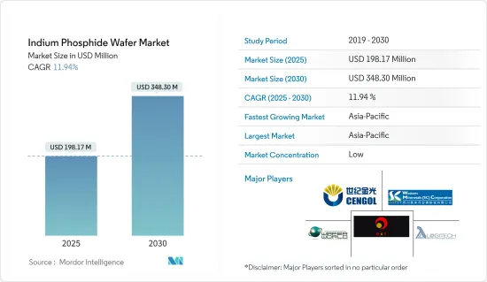
인화인듐 웨이퍼 시장 규모는 2025년에 1억 9,817만 달러로 추정되며, 예측 기간 중(2025-2030년) CAGR은 11.94%로, 2030년에는 3억 4,830만 달러에 달할 것으로 예측됩니다.
인화인듐(InP)은 고효율 레이저, 변조기, 고감도 광검출기를 생성하는 특성을 가지고 있습니다. 또한 레이저 신호를 생성하고 그 신호를 전자 형태로 변환하여 식별할 수 있습니다. 이들은 기업 네트워크 및 데이터센터, 장거리 광섬유 연결, 3G, 5G, LTE 기지국 무선 연결, 위성 통신 등에 사용됩니다. 이러한 요구 사항 증가가 시장을 주도하고 있습니다.
주요 하이라이트
- 인화인듐 웨이퍼는 차량용 LiDAR, 3D 센싱, 소비자 웨어러블, 통신 분야의 데이터 통신 성장에 점점 더 많이 사용되고 있습니다. 이는 예측 기간 중 시장을 촉진할 것으로 예측됩니다. InPinc의 주요 용도로는 5G 통신, 빛과 레이저를 사용하는 데이터센터 연결, 광섬유 레이저 및 검출기, 군용 통신 및 5G 통신에 사용되는 실리콘 포토닉스, RF 증폭기, 스위치, 건강 분야의 적외선 열화상 등이 있습니다.
- 광전자 장비로 알려진 전자 부품은 빛을 감지하고 조절하는 역할을 합니다. 광전자 장비는 전기 정보를 적외선이나 가시광선 에너지로 변환하거나 그 반대의 경우도 마찬가지입니다. 광전자는 태양광발전, 광섬유 통신 시스템, 모니터 및 제어 회로, 전기 안구 등에 활용되고 있습니다. 광전자 부품은 양자 캐스케이드 레이저 및 유도 방출용 주입 레이저 다이오드에 사용되며, LED 및 이미지 센서는 디지털 이미지 시스템, 포장 및 안전 용도에 활용됩니다.
- 2020년 11월 발표된 에릭슨 모빌리티 보고서에 따르면 2020년 말까지 전 세계 모바일 데이터 트래픽은월약 51EB(엑사바이트)에 달할 것으로 추정됩니다. 이는 거의 4.5배 성장하여 2026년에는월226EB에 달할 것으로 예측됩니다. 이 수치는 60억 명 이상의 사람들이 스마트폰, 노트북, 수많은 새로운 디바이스를 통해 한 번에 소비하는 모바일 데이터를 나타냅니다.
- 반도체 실리콘 웨이퍼는 전자 산업의 기반이자 많은 마이크로 전자 장비의 주요 부품입니다. 현재 기술 상황의 발전, 전자기기의 이동성, 디지털화에 따라 이러한 아이템은 다양한 디바이스에 사용되고 있습니다. 또한 소형화된 가젯에 대한 요구가 증가함에 따라 하나의 장비에서 추가 기능에 대한 요구가 급격히 증가하여 실리콘 웨이퍼의 가격이 상승하고 있습니다.
- COVID-19 팬데믹으로 인해 전 세계 대부분의 지역에서 봉쇄 조치가 이어지면서 반도체 제조 장비 업계에서는 일부 품목의 생산이 중단되었습니다. 봉쇄 조치는 소비자 전자제품 수요를 감소시켜 반도체 부문에 전 세계적인 영향을 미쳤습니다. 자동차의 세계 수요와 수출 선적의 지속적인 감소는 반도체 시장에 부정적인 영향을 미쳐 현재 반도체 제조 장비 수요를 둔화시키고 있습니다.
인화인듐 웨이퍼 시장 동향
시장을 선도하는 CE(Consumer Electronics) 분야
- 웨어러블 기술은 일상 활동에 전자제품을 통합하고 신체 어느 부위에나 착용할 수 있는 기능으로 라이프스타일의 변화에 대응하는 개발 동향 중 하나입니다. 인터넷 연결, 네트워크와 기기 간 데이터 교환 옵션 제공 등의 동향이 웨어러블 기술 동향으로 이어지고 있습니다.
- 시스코시스템즈에 따르면 전 세계에서 연결된 웨어러블 기기의 수는 3년 동안 두 배로 증가하여 2016년 3억 2500만 대에서 2019년 7억 2,200만 대에 달할 것이며, 2022년에는 10억 대를 넘어설 것으로 예측됩니다.
- 또한 일본 총무성에 따르면 2021년 현재 일본 가구의 7% 이상이 웨어러블 단말기를 소유하고 있다고 합니다. 웨어러블 단말기의 가구 보급률은 조사 기간(2014-2021년) 동안 꾸준히 상승하여 2014년 0.5%에서 2020년에는 5%로 상승했습니다.
- 전 세계에서 도시화율이 높아짐에 따라 하나의 기기에서 여러 기능을 사용할 수 있고, 시간표를 확인할 수 있는 등 소비자의 요구를 충족시킬 수 있는 고급스럽고 심미적으로 매력적인 제품에 대한 수요가 증가하고 있습니다. 또한 전 세계 수많은 밀레니얼 세대가 근무 시간 추적과 사치품에 대한 지출 능력 증가로 인해 스마트워치를 빠르게 채택하고 있습니다.
- 예를 들어 에릭슨에 따르면 전 세계 스마트폰 계약 수는 2020년 59억 2,400만 대에서 2021년 62억 5,900만 대로 급증했으며, 2027년에는 76억 9,000만 대에 달할 것으로 추산되고 있습니다.
- 또한 노키아의 연례 모바일 브로드밴드 인덱스 보고서 2022에 따르면 4G 지원 기기 생태계가 확대되면서 4G 가입자와 데이터 소비 증가를 주도하고 있습니다. 인도는 2021년에 3,000만 대의 5G 단말기를 포함해 1억 6,000만 대 이상의 스마트폰 출하량으로 사상 최고치를 기록했으며, 활성 4G 지원 단말기는 80% 이상, 활성 5G 지원 단말기는 1,000만 대를 넘어섰습니다. 또한 노키아 보고서는 2025년까지 스마트폰 사용자의 60-75%까지 보급이 확대될 것으로 예측했습니다.
아시아태평양이 급성장 시장으로 부상할 전망
- 아시아태평양은 TSMC, Samsung Electronics와 같은 대기업을 보유하고 있으며, 반도체 주조 분야에서 전 세계에서 큰 점유율을 차지하고 있습니다. 대만, 한국, 일본, 중국도 이 지역에서 큰 비중을 차지하고 있습니다. 미국 반도체산업협회(SIA)에 따르면 1990-2020년까지 전 세계 웨이퍼 팹 설치 용량에서 미국의 점유율은 지속적으로 감소하고 있습니다. 같은 기간 중 아시아에서 새로운 반도체 공장이 빠르게 개발되어 현재 전 세계 생산 능력의 상당 부분을 차지하게 되었습니다.
- 중국은 1,500억 달러의 자금을 바탕으로 국내 IC 산업을 발전시키고 더 많은 칩을 생산할 계획으로 매우 야심찬 반도체 아젠다를 가지고 있습니다. 홍콩, 중국, 대만을 포함한 중화권은 지정학적으로 핫스팟입니다. 미국과 중국의 무역 전쟁은 주요 공정 기술이 집중된 이 지역의 긴장을 더욱 고조시켰고, 많은 중국 기업이 반도체 파운드리에 투자할 수밖에 없었습니다.
- 2021년 3월에 발표된 중국의 2021-2025년 신 5개년 계획에서 기초연구 강화가 중요한 우선순위에 포함되었습니다. 중앙정부의 기초연구에 대한 지출은 2021년에 11% 증가할 것으로 예상되며, 이는 전체 R&D 투자 계획인 7%와 GDP 성장률 목표인 6%를 크게 상회하는 수치입니다. 반도체는 자금과 자원의 우선순위 7대 분야 중 하나로 지정되었습니다. 설계에 종사하는 기업은 컴퓨팅, 스토리지, 네트워크 접속, 전력 관리 등 전자기기를 작동시키는 중요한 작업을 수행하는 나노미터 단위의 집적회로를 개발합니다. 칩 수요 증가로 2021년에는 이익이 두 배 이상 증가할 것으로 예측됩니다. 중국의 주요 반도체 파운드리은 2022년 역량 개발을 위해 사상 최대 금액을 확보했습니다. 올해 Semiconductor Manufacturing International Corp(SMIC)는 자본 지출에 50억 달러를 확보하여 2021년45억 달러에서 증가했습니다.
- 중국은 7nm 칩 생산 자립에 크게 다가서고 있습니다. 중국은 7nm 칩 제조 공정에서 비약적인 발전을 이루며 해외 장비 및 재료 공급업체에 대한 의존도를 낮추기 위한 노력의 일환으로 제조 공정의 여러 부문에서 툴와 노하우를 개발하고 있는 것으로 알려졌습니다.
- 연구 및 제휴의 현저한 확장은 시장 성장률을 더욱 높일 것입니다. 예를 들어 LioniX International(LXI)과 Institute of Microelectronics Chinese Academy of Science(IMECAS)는 광집적회로(PIC) 플랫폼의 파트너십을 확대하기로 합의했습니다. PIC에서 중요한 플랫폼으로는 SOI(Silicon On Insulator), InP(Indium Phosphide), 질화규소 기반 TriPleXplatform이 있습니다. 가 있습니다. 이들 플랫폼은 멀티 프로젝트 웨이퍼(MPW) 액세스를 통해 이용할 수 있습니다.
인화인듐 웨이퍼 산업 개요
인화인듐 웨이퍼 제조 분야에서는 대형 제조업체의 존재감이 커지고 있으며, 예측 기간 중 경쟁 업체 간의 적대적 관계가 심화될 것으로 예상되며, JX Nippon Mining & Metals 및 Powerway Advanced Materials와 같은 시장 기존 업체는 시장 전체에 상당한 영향을 미치고 있습니다.
- 2022년 3월: 인텔은 독일에 두 번째 칩 제조 기지인 '메가 팹'을 신설할 계획을 발표했습니다. 2021년 8월, ACM Research Inc.는 베벨 에칭 제품을 출시하여 ACM의 종합적인 습식 툴 제공을 더욱 확대했습니다. 이 툴은 후속 공정 공정에서 에지 오염의 영향을 최소화하고 칩 제조 수율을 향상시킬 수 있습니다.
- 2022년 2월: 캐나다 정부는 캐나다 반도체 및 포토닉스 산업에 대한 대규모 투자를 발표했으며, 2억 4,000만 캐나다 달러의 투자를 통해 캐나다는 포토닉스의 세계 리더로서의 역할을 확고히 하고 반도체 개발 및 제조를 강화할 것입니다. 캐나다에는 100개 이상의 국내외 반도체 기업이 마이크로칩 연구개발에 매진하고 있습니다. 화합물 반도체, 미세전자기계시스템(MEMS), 첨단 포장 등의 분야에는 30개 이상의 응용 연구소와 5개의 상업시설이 있습니다.
기타 특전:
- 엑셀 형식의 시장 예측(ME) 시트
- 3개월간의 애널리스트 지원
목차
제1장 서론
- 조사의 전제조건과 시장 정의
- 조사 범위
제2장 조사 방법
제3장 개요
제4장 시장 인사이트
- 시장 개요
- 업계의 매력 - Porter's Five Forces 분석
- 공급 기업의 교섭력
- 구매자/소비자의 교섭력
- 신규 진출업체의 위협
- 대체품의 위협
- 경쟁 기업 간 경쟁 관계
- 산업 밸류체인 분석
- 기술 스냅숏
- 업계에 대한 COVID-19의 영향 평가
제5장 시장 역학
- 시장 성장 촉진요인
- 광전자 디바이스의 사용 증가
- 데이터 통신 비즈니스와 5G의 성장
- 시장 성장 억제요인
- 기타 대체품과의 경쟁
제6장 시장 세분화
- 직경별
- 50.8mm 또는 2인치
- 76.2mm 또는 3인치
- 100mm 또는 4인치 이상
- 최종사용자 산업별 용도
- CE(Consumer Electronics)
- 통신 기기
- 의료
- 기타 최종사용자 산업
- 지역별
- 북미
- 유럽
- 아시아태평양
- 세계의 기타 지역
제7장 경쟁 구도
- 기업 개요
- AXT Inc.
- Wafer World Inc.
- Logitech Ltd.
- Western Minmetals(SC) Corporation
- Century Goldray Semiconductor Co. Ltd
- Semiconductor Wafer Inc.
- Ding Ten Industrial Inc.
- Sumitomo Electric Semiconductor Materials Inc.(Sumitomo Electric Industries Ltd)
- Xiamen Powerway Advanced Material Co. Ltd
- JX Nippon Mining & Metals Corporation(Eneos Holdings Inc.)
제8장 투자 분석
제9장 시장 기회와 향후 동향
KSA 25.05.14The Indium Phosphide Wafer Market size is estimated at USD 198.17 million in 2025, and is expected to reach USD 348.30 million by 2030, at a CAGR of 11.94% during the forecast period (2025-2030).

Indium phosphide (InP) has properties that produce highly efficient lasers, modulators, and sensitive photodetectors. It can also generate laser signals and convert and identify those signals back to the electronic form. These are used for company networks and data centers, long-haul optical fiber connections over far distances, wireless connections for 3G, 5G, and LTE base stations, and satellite communication. The growth in such requirements is driving the market.
Key Highlights
- Indium phosphide wafers are increasingly adopted in the manufacture of LiDAR for automotive, 3D sensing, consumer wearables, and the growth in datacom in the telecommunication sector. This is expected to drive the market during the forecast period. In addition, some of the major applications of InPinclude 5G communications, data center connectivity that uses lights and lasers, fiber optic lasers and detectors, silicon photonics, RF amplifiers, and switches used in military and 5G communications, and infrared thermal imaging in health.
- Electronic components known as optoelectronic devices detect and regulate light. They convert electrical information into infrared or visible energy and vice versa. It is utilized in photovoltaic power supply, optical fiber communication systems, monitor and control circuits, and electric eyes. Optoelectronic components are used in quantum cascade lasers and injection laser diodes for stimulated emission. LEDs and image sensors are utilized in digital imaging systems, packaging, and safety applications.
- According to the Ericsson Mobility Report published in November 2020, the global mobile data traffic was estimated to reach around 51 EB (exabytes) per month by the end of 2020. This was projected to grow by a factor of almost 4.5 to reach 226 EB per month in 2026. This figure represents the mobile data that will be consumed by greater than 6 billion people using smartphones, laptops, and a multitude of new devices at a time.
- The semiconductor silicon wafer serves as the foundation of the electronics industry and is the main component of many microelectronic devices. With the current advances in the technology landscape, electronic mobility, and digitalization, these items are finding use in a wide range of devices. The requirement for additional capability from a single device has also grown dramatically as a result of the need for small-sized gadgets, which boosts the price of the silicon wafer.
- The COVID-19 pandemic has halted the manufacturing of several items in the semiconductor production equipment industry owing to the continued lockdown in most regions across the world. Lockdown measures reduced the demand for consumer electronic gadgets, which had a global impact on the semiconductor sector. The continued decline in worldwide demand and export shipments for automobiles caused a negative impact on the semiconductor market, which is currently slowing down the demand for semiconductor manufacturing equipment.
Indium Phosphide Wafer Market Trends
Consumer Electronics Segment Expected to Drive the Market
- Wearable technology, a developing trend, integrates electronics into daily activities and addresses the changing lifestyles with the ability to be worn on any part of the body. Factors such as the ability to connect to the internet and provide data exchange options between a network and a device are leading to the trend of wearable technology.
- According to Cisco Systems, the number of connected wearable devices globally has doubled in the span of three years, increasing from 325 million in 2016 to 722 million in 2019. The number of devices is forecasted to be over 1 billion by 2022.
- Further, according to the Ministry of Internal Affairs and Communications (Japan), as of 2021, over 7% of households in Japan owned a wearable device. The household penetration rate of wearable devices steadily increased throughout the surveyed period (2014-2021), rising from 0.5% in 2014 to 5% in 2020.
- The rising rates of urbanization in various parts of the world have driven the demand for advanced, aesthetically appealing products that possess the ability to serve the consumers' requirements better, such as multiple features in one device and time schedules. Moreover, the vast millennial population across the globe has been quick to adopt smartwatches, owing to the increased spending ability on their regular work hours tracking and luxury standards.
- For instance, according to Ericsson, the number of smartphone subscriptions worldwide witnessed an upsurge from 5,924 million in 2020 to 6,259 million in 2021. The number is estimated to reach 7,690 million in 2027.
- Further, according to the Nokia annual mobile broadband index report 2022, the growing ecosystem of 4G-capable devices is driving the growth in 4G subscribers and data consumption. India recorded the highest-ever shipment of over 160 million smartphones, including 30 million 5G devices, in 2021, with active 4G capable devices crossing 80% and the number of active 5G capable devices crossing 10 million. The Nokia report also forecasted that user adoption will increase to 60-75% of the smartphone user base by 2025.
Asia-Pacific Expected to be the Fastest-growing Market
- The Asia-Pacific region commands a prominent share of semiconductor foundries globally, with major companies such as TSMC and Samsung Electronics. Taiwan, South Korea, Japan, and China have a significant market share in the region. According to the US Semiconductor Industry Association (SIA), the US share of the global installed wafer fab capacity constantly declined from 1990 to 2020. During the same period, Asia saw a meteoric rise in developing new fabs to the point where it now accounts for a significant share of the world's capacity.
- China has a very ambitious semiconductor agenda. Backed by USD 150 billion in funding, the country is developing its domestic IC industry and plans to make more of its chips. Greater China, which encompasses Hong Kong, China, and Taiwan, is a geopolitical hotspot. The US-China trade war is compounding tensions in an area where all the leading process technology is located, forcing many Chinese companies to invest in their semiconductor foundries.
- China's new five-year plan for 2021-2025, announced in March 2021, established that boosting basic research was a critical priority. The central government's spending on basic research was expected to increase by 11% in 2021, well above the 7% planned for the overall R&D investment and the 6% target for GDP growth. Semiconductors were designated as one of the seven areas that will be given priority in terms of funding and resources. Firms involved in design develop nanometer-scale integrated circuits that perform the critical tasks that make electronic devices work, such as computing, storage, network connectivity, and power management. The profit was estimated to more than double in 2021 because of the robust chip demand. China's leading semiconductor foundry set aside a record sum for capacity development in 2022. This year, Semiconductor Manufacturing International Corp (SMIC) set aside USD 5 billion for capital spending, up from USD 4.5 billion in 2021.
- China is moving significantly closer to self-reliance in 7 nm chip production. China has made breakthroughs in its 7 nm chip-making process, reportedly developing tools and know-hows for several segments of the manufacturing process amid efforts to reduce reliance on foreign equipment and material vendors.
- The significant research and partnership growth further bolsters the market growth rate. For instance, LioniXInternational (LXI) and the Institute of Microelectronics Chinese Academy of Science (IMECAS) agreed to expand their Photonic Integrated Circuit (PIC) platform partnership by actively supporting the functionality and offering both platforms. The critical platforms in the PIC landscape include Silicon On Insulator (SOI), Indium Phosphide (InP), and the silicon nitride-based TriPleXplatform. These platforms are available through Multi-Project Wafer (MPW) access.
Indium Phosphide Wafer Industry Overview
The growing presence of large manufacturers in the indium phosphide wafer manufacturing sector is expected to intensify competitive rivalry during the forecast period. Market incumbents, such as JX Nippon Mining & Metals Corporation and Powerway Advanced Material Co. Ltd, considerably influence the overall market.
- March 2022: Intel revealed plans for a second new 'Megafab," a chipmaking site in Germany, with an expected USD 88 billion in investments across several European countries. Further, in August 2021, ACM Research Inc. launched its Bevel Etch product, which further expanded ACM's comprehensive offering of wet tools. This tool minimizes the impact of edge contamination for subsequent process steps and improves chip manufacturing yield.
- February 2022: The Government of Canada announced a significant investment in the Canadian semiconductor and photonics industries. The investment of CAD 240 million will help solidify Canada's role as a global leader in photonics and will bolster the development and manufacturing of semiconductors. Over 100 domestic and international semiconductor companies work on microchip research and development in Canada. There are over 30 applied research laboratories and five commercial facilities for areas including compound semiconductors, microelectromechanical systems (MEMS), and advanced packaging.
Additional Benefits:
- The market estimate (ME) sheet in Excel format
- 3 months of analyst support
TABLE OF CONTENTS
1 INTRODUCTION
- 1.1 Study Assumptions and Market Definition
- 1.2 Scope of the Study
2 RESEARCH METHODOLOGY
3 EXECUTIVE SUMMARY
4 MARKET INSIGHTS
- 4.1 Market Overview
- 4.2 Industry Attractiveness - Porter's Five Forces Analysis
- 4.2.1 Bargaining Power of Suppliers
- 4.2.2 Bargaining Power of Buyers/Consumers
- 4.2.3 Threat of New Entrants
- 4.2.4 Threat of Substitute Products
- 4.2.5 Intensity of Competitive Rivalry
- 4.3 Industry Value Chain Analysis
- 4.4 Technology Snapshot
- 4.5 Assessment of the Impact of COVID-19 on the Industry
5 MARKET DYNAMICS
- 5.1 Market Drivers
- 5.1.1 Increasing Use of Optoelectronic Devices
- 5.1.2 Growth of Datacom Business and 5G
- 5.2 Market Restraints
- 5.2.1 Competition from Other Substitutes
6 MARKET SEGMENTATION
- 6.1 By Diameter
- 6.1.1 50.8 mm or 2 "
- 6.1.2 76.2 mm or 3 "
- 6.1.3 100 mm or 4" and Above
- 6.2 By End-user Industry Application
- 6.2.1 Consumer Electronics
- 6.2.2 Telecommunications
- 6.2.3 Medical
- 6.2.4 Other End-user Industry Applications
- 6.3 By Geography
- 6.3.1 North America
- 6.3.2 Europe
- 6.3.3 Asia-Pacific
- 6.3.4 Rest of the world
7 COMPETITIVE LANDSCAPE
- 7.1 Company Profiles
- 7.1.1 AXT Inc.
- 7.1.2 Wafer World Inc.
- 7.1.3 Logitech Ltd.
- 7.1.4 Western Minmetals (SC) Corporation
- 7.1.5 Century Goldray Semiconductor Co. Ltd
- 7.1.6 Semiconductor Wafer Inc.
- 7.1.7 Ding Ten Industrial Inc.
- 7.1.8 Sumitomo Electric Semiconductor Materials Inc. (Sumitomo Electric Industries Ltd)
- 7.1.9 Xiamen Powerway Advanced Material Co. Ltd
- 7.1.10 JX Nippon Mining & Metals Corporation (Eneos Holdings Inc.)