|
시장보고서
상품코드
1940553
첨단 IC 기판 : 시장 점유율 분석, 업계 동향과 통계, 성장 예측(2026-2031년)Advanced IC Substrates - Market Share Analysis, Industry Trends & Statistics, Growth Forecasts (2026 - 2031) |
||||||
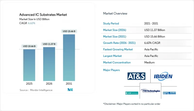
첨단 IC 기판 시장은 2025년 106억 6,000만 달러에서 2026년에는 113억 7,000만 달러로 성장하며, 2026-2031년에 CAGR 6.63%로 추이하며, 2031년까지 156억 6,000만 달러에 달할 것으로 예측됩니다.

수요는 전통적 컴퓨팅에서 더 많은 레이어 수, 더 미세한 선폭, 더 엄격한 워프 제어가 필요한 AI 중심 워크로드로 결정적으로 전환되었습니다. 아시아태평양의 기판 벤더들은 이미 대량의 ABF 생산 능력과 파운드리 패키징 라인과의 긴밀한 관계를 보유하고 있었기 때문에 이러한 전환의 혜택을 누릴 수 있었습니다. 주요 클라우드 서비스 제공 업체는 2025년까지 CoWoS 및 FC-BGA의 안정적인 공급을 보장하기 위해 장기 구매 계약을 가속화하여 기판 제조업체의 가격 결정력을 더욱 강화했습니다. 동시에, 유리 코어 기술 개발이 성숙해지면서 2020년대 후반 상용화가 예정된 초고밀도 패키지용 ABF의 전략적 대안이 만들어졌습니다.
세계 첨단 IC 기판 시장 동향 및 인사이트
AI/HPC 가속기용 ABF 기판에 대한 수요 급증
2025년 생성형 AI 서버의 대규모 도입으로 아지노모토 빌드업 필름공급이 타이트해집니다. ABF 패널의 리드타임은 35주 이상이며, 현물 가격은 2024년 계약 수준 대비 최대 25%의 프리미엄이 발생했습니다. 대만공급업체인 유니미크론, 킨사스, 난야 PCB는 장기간의 재고 조정을 마친 후 두 자릿수 매출 성장을 회복했으나, 수요에 대응하기 위해 가동률은 여전히 90%에 머물러 있습니다. Samsung Electronics는 2025년 2분기에 AI용 ABF 생산량을 늘리고, 유리 코어의 파일럿 생산을 시작했습니다. 이는 단일 소재 리스크를 줄이기 위한 이중 소싱 전략을 반영한 것입니다. TSMC는 CoWoS의 연간 생산량을 두 배로 늘릴 계획을 밝혔는데, 이는 기판 수요가 기존 생산능력을 크게 상회할 것임을 시사하고 있습니다. 이러한 움직임으로 공급 부족은 20%로 확대되었고, 기판 제조업체들은 2026년 신규 라인이 가동되기 전까지는 공급 부족이 해소되지 않을 것으로 예상하고 있습니다.
미세화 및 이기종 통합 동향
칩렛 아키텍처, 코어리스 인터포저, 실리콘 관통전극(TSV) 기술은 패키지 설계 규칙을 재정의하여 생산 환경에서 기판 선폭을 10µm 이하로 낮췄습니다. 어플라이드 머티어리얼즈는 디스크리트 칩렛의 온패키지 통합이 모놀리식 다이 방식에 비해 와트당 성능이 뛰어나다고 강조했습니다. Toppan은 기존 ABF 솔루션보다 열팽창 계수가 45% 낮은 코어리스 유기 인터포저를 출시하여 멀티 다이 적층 내부의 기계적 응력을 감소시켰습니다. 브로드컴의 3.5D XDSiP 기술은 6,000mm2 이상의 실리콘과 12층 HBM 스택을 통합하여 한정된 면적에 수천 개의 고속 신호를 배선할 수 있는 기판에 대한 수요를 부각시켰습니다. TSMC와 ASE는 스테퍼 효율을 높이고 평방인치당 비용을 절감하기 위해 최대 310×310mm의 패널 레벨 패키징 라인에 투자했습니다. 이러한 변화로 인해 첨단 IC 기판 시장은 차세대 컴퓨팅 밀도를 실현하는 중요한 기반 기술로 자리매김하고 있습니다.
ABF 기판 공급 부족 및 리드 타임 급증
2024-2025년까지 ABF 패널의 지속적인 공급 부족으로 첨단 IC 기판 시장의 상승을 억제했습니다. ABF 수지를 거의 독점적으로 공급하고 있는 아지노모토는 2026년 신규 수지 반응 설비가 가동될 때까지 20%의 수급 격차가 지속될 것으로 예상하고 있습니다. TSMC가 CoWoS 수요의 80%만 충족할 수 있다고 밝힌 만큼, 파운드리 업체들도 이러한 제약이 있음을 확인했습니다. 적층화학에 대한 의존도를 탈피하고자 하는 積水化? 등 경쟁사도 있었지만, 하이엔드 AI 패키지의 인증 주기로 인해 도입이 늦어졌습니다. 낮은 팽창계수로 평가되는 T-Glass 코어 소재의 동시 부족으로 인해 닛토방의 생산능력 확장이 지연되어 리드타임이 급증하게 되었습니다. 기판 제조업체는 인라인 측정 기술을 도입하여 초기 수율 향상과 기존 설비의 효율화를 위해 노력하고 있으며, 대부분의 고객들은 2025년까지 할당 프로그램 대상에 포함되었습니다.
부문 분석
FC-BGA 기판은 2025년 첨단 IC 기판 시장 점유율의 44.32%를 차지했습니다. 그 우위는 AI 가속기 및 서버 CPU가 요구하는 검증된 전기적 성능에서 비롯됩니다. GPU 제조업체들이 생산 능력 확보를 서두르면서 가동률은 2025년 내내 높은 수준을 유지했습니다. 그러나 자동차 도메인 컨트롤러와 접이식 모바일 기기용 리지드 플렉스 CSP 라인으로 성장의 중심이 옮겨갔습니다. 리지드 플렉스의 출하량은 CAGR 7.94%로 증가했으며, 굽힘 반경과 제어 임피던스의 균형을 유지할 수 있는 새로운 적층 기판 공급업체를 유치했습니다. FC-CSP는 중급형 모바일 프로세서에 대한 공급을 지속했으나, 원가 압박으로 인해 평균 판매 가격 상승은 제한적이었습니다. 유기 BGA/LGA는 레거시 데스크톱 플랫폼에서는 여전히 중요하지만, 설계 채택은 플립칩 방식에 자리를 내주었습니다. 패널 레벨 FC 기판('기타'로 분류)은 TSMC와 ASE에서 시험 생산이 시작되어 패널 당 7배의 사용 가능 면적을 실현하여 새로운 규모의 경제를 개발했습니다.
FC-BGA는 CoWoS 적층의 주요 기반이 되었습니다. 설계자의 14-26층에 대한 요구가 증가하여 위치결정 공차가 더욱 엄격해졌습니다. 이에 따라 기판 제조업체는 AI 탑재 광학 검사 장비를 도입하여 적층 초기 단계의 비아 및 배선 위치 이탈을 조기에 감지할 수 있도록 했습니다. 리지드플렉스 CSP는 자동차 제조업체들이 인포테인먼트 유닛을 15인치 곡면 디스플레이로 전환하면서 수요가 확대되었습니다. 이 디스플레이는 Z축 방향의 유연성이 필요했기 때문입니다. 접이식 단말기에 카메라 통합이 증가하면서 추가 수요를 창출했습니다. 이러한 추세에 따라 리지드 플렉스 기판은 2031년까지 지속적인 시장 침투가 예상되며, FC-BGA는 첨단 IC 기판 시장에서 고부가가치 포지션을 계속 유지할 것으로 보입니다.
2025년 기준, ABF는 첨단 IC 기판 시장 규모의 60.35%를 차지했습니다. 아지노모토의 독자적인 수지 배합 기술로 2.5D 및 3D 적층에서 고객이 신뢰할 수 있는 일관된 유전체 성능과 드릴 가공성을 확립했습니다. 2025년 각 공급업체들이 ABF 혼합라인을 증설했으나, 생산량 증가가 수요 증가를 따라잡지 못하면서 판매자 우위가 강화되었습니다. 유리 기판은 2025년 출하량의 2% 미만이지만 13.58%의 예측 CAGR을 기록했습니다. 200mm×200mm 플레이트에서 ±5μm 이내의 평탄도를 실현하여 ABF보다 미세한 재배선층과 높은 I/O 밀도를 가능하게 했습니다. 인텔의 자체 개발 철수는 서드파티 유리 공급업체들의 신뢰성을 지원하고, 생태계 구축을 가속화했습니다.
BT 수지는 기판 온도가 150℃에 이르는 것이 일반적인 자동차 제어 장치에서 여전히 유용성을 유지했습니다. 세라믹 및 LTCC 부문은 연속적인 열 사이클에 노출되는 파워 디바이스에 공급되며, ABF 라인이 과잉 판매될 경우 매출 완충 역할을 했습니다. 유리 코어의 인증에서는 비아 형성의 균일성에 문제가 발생했으나, 초기 시제품에서는 리플로우시 휨 특성이 양호한 것으로 나타났습니다. AMD가 2026년 CPU 플랫폼의 유리화 의사를 밝힘에 따라 기판 제조업체들은 양산 시작 전 생산 물량 확보를 서두르는 움직임을 보이고 있습니다. 수율이 유지된다면, 2031년까지 유리 기판의 매출 점유율은 5.3%에 육박하거나 그 이상에 도달할 수 있을 것으로 예측됩니다.
첨단 IC 기판 시장은 기판 유형(FC-BGA, FC-CSP, 유기 BGA/LGA 등), 핵심 재료(ABF, BT, 유리 등), 패키징 기술(2D 플립칩, 2.5D 인터포저 등), 디바이스 노드(28nm 이상, 16/14-10nm 등), 최종사용 산업(모바일, 민수, 자동차, 가전 등), 지역(북미, 유럽, 중국, 일본 등)으로 세분화됩니다. ), 최종사용 산업(모바일/민생, 자동차/운송 등), 지역(북미, 남미, 유럽, 아시아태평양, 중동/아프리카)으로 구분되어 있습니다.
지역별 분석
아시아태평양은 2025년 첨단 IC 기판 시장에서 68.35%의 점유율을 차지할 것으로 예측됩니다. 대만의 유니크론, 킨서스, 난야 PCB는 2023년 출하량을 압박한 재고 조정 대신 AI 서버 수요가 견인하면서 2025년 두 자릿수 성장을 달성했습니다. 일본에서는 3조 9,000억 엔(255억 달러)의 보조금 지원을 받아 TSMC 구마모토 공장을 중심으로 규슈의 패키징 거점으로서의 위상을 재확립했습니다. 한국은 2030년까지월770만장 웨이퍼 스타트 달성을 목표로 4,710억 달러 규모의 통합 클러스터 계획을 발표했으며, 로직 공장에 인접한 ABF-CoWoS 라인 설치를 계획하고 있습니다. 중국은 플립칩 및 SiP(시스템온패키지) 생산능력 확충을 위해 지역별로 특혜를 도입했으나, 수출규제로 인해 제조장비 조달이 제한되어 유리코어 채택이 지연되고 있습니다.
북미에서는 CHIPS법에 기반한 첨단인 현지화 진행. TSMC의 애리조나 캠퍼스는 리스크 분산을 위해 ABF 라인을 갖춘 6공장 체제로 전환했습니다. 엔테그리스는 기판 구리 도금용 여과재에 대해 최대 7,500만 달러의 연방정부 지원을 받았습니다. OSAT 업체들은 방산용 칩 패키징 수요에 대응하기 위해 미국 확장을 검토하고 있지만, 임금 상승이 우려되는 상황입니다.
유럽은 자동차 및 파워 디바이스에 집중하고 있습니다. 온세미컨덕터 체코 SiC 공장은 역내 인버터 기판의 엔드 투 엔드 공급망을 구축했습니다. 독일과 프랑스는 인텔-TSMC의 파운드리 확장 지원을 위해 공동 ABF 파일럿 라인 설치를 검토. 한편, 베트남, 인도, 말레이시아는 조립 보조금 제도를 추진하고 있습니다. 암콜은 바쿠닌 주에 16억 달러 규모의 공장을 설립했으며, 인도 정부는 CG파워와 르네사스가 주도하는 OSAT 사업에 7,600 루피(9억 1,000만 달러) 규모의 투자를 승인했습니다. 이러한 움직임으로 첨단 IC 기판 시장의 지역적 리스크 분산이 진행되었습니다.
기타 특전:
- 엑셀 형식 시장 예측(ME) 시트
- 애널리스트의 3개월간 지원
자주 묻는 질문
목차
제1장 서론
제2장 조사 방법
제3장 개요
제4장 시장 구도
제5장 시장 규모와 성장 예측
제6장 경쟁 구도
제7장 시장 기회와 향후 전망
KSA 26.03.06The advanced IC substrates market is expected to grow from USD 10.66 billion in 2025 to USD 11.37 billion in 2026 and is forecast to reach USD 15.66 billion by 2031 at 6.63% CAGR over 2026-2031.
Demand shifted decisively from traditional computing toward AI-centric workloads that require higher layer counts, finer linewidths, and tighter warpage control. Asia-Pacific-based substrate vendors benefited from this pivot because they already possessed high-volume ABF capacity and close relationships with foundry packaging lines. Major cloud service providers accelerated long-term purchase agreements in 2025 to secure guaranteed CoWoS and FC-BGA supply, further tilting pricing power to substrate producers. At the same time, glass-core innovation matured, creating a strategic alternative to ABF for ultra-high-density packages scheduled for commercial release in the latter half of the decade.
Global Advanced IC Substrates Market Trends and Insights
Surge in ABF-substrate demand for AI/HPC accelerators
Massive roll-outs of generative-AI servers in 2025 tightened supplies of Ajinomoto Build-up Film, pushing lead-times for ABF panels past 35 weeks and triggering spot-price premiums of up to 25% over 2024 contract levels. Taiwanese suppliers Unimicron, Kinsus, and Nan Ya PCB restored double-digit revenue growth after concluding a prolonged inventory correction, yet still operated at 90% utilization to keep pace with demand. Samsung Electro-Mechanics ramped AI-oriented ABF volume in Q2 2025 and started pilot glass-core runs, reflecting a dual-sourcing strategy aimed at mitigating single-material risk. TSMC disclosed plans to double annual CoWoS output, implying substrate demand well above existing capacity. Collectively, these moves widened a 20% supply gap that substrate makers do not expect to close until fresh lines come online in 2026.
Miniaturization and heterogeneous integration trend
Chiplet architectures, coreless interposers, and through-silicon vias redefined package design rules and pushed substrate line-widths below 10 µm in production settings. Applied Materials highlighted that on-package integration of discrete chiplets delivered superior performance per watt compared with monolithic die approaches. TOPPAN unveiled a coreless organic interposer with a 45% lower coefficient of thermal expansion than legacy ABF solutions, easing mechanical stress inside multi-die stacks. Broadcom's 3.5D XDSiP technology integrated more than 6,000 mm2 of silicon and 12 HBM stacks, underscoring the demand for substrates that can route thousands of high-speed signals in confined footprints. TSMC and ASE invested in panel-level packaging lines up to 310 X 310 mm to gain stepper efficiency and reduce cost per square inch. These shifts position the advanced IC substrates market as a pivotal enabler for next-generation compute density.
ABF-substrate capacity shortage and lead-time spikes
A persistent deficit in ABF panel output restricted upside for the advanced IC substrates market during 2024-2025. Ajinomoto, the near-monopoly supplier of ABF resin, acknowledged a 20% demand-supply gap that would remain until new resin reactors started in 2026. Foundries confirmed the constraint when TSMC said it could satisfy only 80% of CoWoS demand. Competitors such as Sekisui Chemical aimed to break dependence on alternate build-up chemistries, yet qualification cycles for high-end AI packages slowed adoption. Parallel shortages of T-Glass core material, prized for low expansion coefficients, delayed capacity expansions at Nittobo, compounding lead-time spikes. Substrate makers deployed inline metrology to raise first-pass yield and stretch existing capacity, but most customers still entered allocation programs through 2025.
Other drivers and restraints analyzed in the detailed report include:
- 5G build-out boosting high-frequency RF packaging
- Automotive-EV electrification needs high-reliability substrates
- High capital intensity and process complexity
For complete list of drivers and restraints, kindly check the Table Of Contents.
Segment Analysis
FC-BGA substrates accounted for 44.32% of the advanced IC substrates market share in 2025. Their lead is derived from proven electrical performance required by AI accelerators and server CPUs. Utilization stayed high through 2025 as GPU makers rushed to secure capacity. Growth, however, shifted toward rigid-flex CSP lines that served automotive domain controllers and foldable mobile devices. Rigid-flex volume increased at an 7.94% CAGR, attracting new laminate suppliers able to balance bend radius with controlled impedance. FC-CSP continued to service mid-tier mobile processors, but its cost pressures limited ASP upside. Organic BGA/LGA remained relevant for legacy desktop platforms, yet ceded design wins to flip-chip options. Panel-level FC substrates, still counted under "Others," emerged in pilot volumes at TSMC and ASE, promising 7X usable area per panel and opening new economies of scale.
FC-BGA stayed the workhorse for CoWoS build-ups. Designers demanded 14-26 layer counts, forcing tighter registration tolerances. In response, substrate makers installed AI-enabled optical inspection to catch via-to-trace violations early in the stack. Rigid-flex CSP benefited when automakers migrated infotainment units to 15-inch curved displays that required Z-axis flexibility. Increased camera integration in foldables presented an additional pull. These dynamics support sustained penetration for rigid-flex through 2031 while FC-BGA continues to anchor high-value positions within the advanced IC substrates market.
ABF represented 60.35% of the advanced IC substrates market size in 2025. Ajinomoto's exclusive resin recipe established consistent dielectric performance and drillability that customers trusted for 2.5D and 3D stacks. Suppliers expanded ABF mixing rooms in 2025, but output gains lagged demand growth, reinforcing seller leverage. Glass substrates, though less than 2% of 2025 shipments, recorded a 13.58% forecast CAGR. Flatness within +-5 µm across 200 mm x 200 mm plates allowed finer redistribution layers and higher I/O density than ABF. Intel's exit from in-house development validated third-party glass suppliers and accelerated ecosystem readiness.
BT resin preserved relevance in automotive control units where 150 °C board temperatures were common. Ceramic and LTCC segments supplied power devices exposed to continuous thermal cycling and offered incremental revenue buffers when ABF lines were oversold. Qualification of glass cores faced hurdles in via formation uniformity, but early builds delivered promising warpage metrics at reflow. AMD signaled its intention to switch its 2026 CPU platforms to glass, encouraging substrate makers to lock capacity slots well ahead of volume ramps. If yields hold, glass could equal or surpass 5.3% revenue share by 2031.
Advanced IC Substrates Market is Segmented by Substrate Type (FC-BGA, FC-CSP, Organic BGA/LGA, and More), Core Material (ABF, BT, Glass, and More), Packaging Technology (2D Flip-Chip, 2. 5D Interposer, and More), Device Node (>=28 Nm, 16/14-10 Nm, and More), End-Use Industry (Mobile and Consumer, Automotive and Transportation, and More), and Geography (North America, South America, Europe, Asia-Pacific, and Middle East and Africa).
Geography Analysis
Asia-Pacific captured 68.35% of the advanced IC substrates market in 2025. Taiwan's Unimicron, Kinsus, and Nan Ya PCB returned double-digit growth in 2025 as AI server demand replaced the inventory correction that weighed on 2023 shipments. Japan's resurgence, backed by JPY 3.9 trillion (USD 25.5 billion) in subsidies, re-established Kyushu as a packaging hub anchored by TSMC's Kumamoto fab. South Korea announced a USD 471 billion integrated cluster plan designed to deliver 7.7 million wafer starts per month by 2030, embedding ABF-CoWoS lines adjacent to logic fabs. China deployed regional incentives to build flip-chip and SiP capacity, but export restrictions narrowed tooling access, slowing glass-core adoption.
North America's advanced localization efforts under the CHIPS Act. TSMC's Arizona campus moved to a six-fab vision with potential ABF lines colocated for risk mitigation. Entegris secured up to USD 75 million in federal support for filtration media used in substrate copper plating. OSAT giants evaluated U.S. expansion to satisfy defense-oriented chip packaging mandates, though wage inflation remained a concern.
Europe focused on automotive and power devices. OnSemi's Czech SiC facility created an end-to-end supply chain for inverter substrates inside the bloc. Germany and France considered joint ABF pilot lines to support foundry expansions by Intel and TSMC. Meanwhile, Vietnam, India, and Malaysia pursued assembly subsidies. Amkor opened a USD 1.6 billion plant in Bac Ninh, and India approved INR 7,600 crore (USD 910 million) for an OSAT venture led by CG Power and Renesas. These moves diversified geographic risk in the advanced IC substrates market.
- ASE Technology Holding Co., Ltd.
- AT&S Austria Technologie & Systemtechnik AG
- Siliconware Precision Industries Co., Ltd.
- TTM Technologies, Inc.
- Ibiden Co., Ltd.
- Kyocera Corporation
- Fujitsu Interconnect Technologies Ltd.
- JCET Group Co., Ltd.
- Panasonic Holdings Corporation
- Kinsus Interconnect Technology Corp.
- Unimicron Technology Corp.
- Nan Ya Printed Circuit Board Corp.
- Samsung Electro-Mechanics Co., Ltd.
- LG Innotek Co., Ltd.
- Simmtech Co., Ltd.
- Shinko Electric Industries Co., Ltd.
- Shennan Circuits Co., Ltd.
- Zhen Ding Technology Holding Ltd.
- Daeduck Electronics Co., Ltd.
- Meiko Electronics Co., Ltd.
- WUS Printed Circuit Co., Ltd.
- Zhejiang Kingdom Sci-Tech Co., Ltd.
- SKC Absolics Inc.
- Tripod Technology Corp.
- Toppan Inc.
Additional Benefits:
- The market estimate (ME) sheet in Excel format
- 3 months of analyst support
TABLE OF CONTENTS
1 INTRODUCTION
- 1.1 Study Assumptions and Market Definition
- 1.2 Scope of the Study
2 RESEARCH METHODOLOGY
3 EXECUTIVE SUMMARY
4 MARKET LANDSCAPE
- 4.1 Market Overview
- 4.2 Market Drivers
- 4.2.1 Surge in ABF-substrate demand for AI/HPC accelerators
- 4.2.2 Miniaturisation and heterogeneous integration trend
- 4.2.3 5G build-out boosting high-frequency RF packaging
- 4.2.4 Automotive-EV electrification needs high-reliability substrates
- 4.2.5 Glass-core substrates unlock >2X layer counts
- 4.2.6 CHIPS-style subsidies tied to substrate fabs
- 4.3 Market Restraints
- 4.3.1 ABF-substrate capacity shortage and lead-time spikes
- 4.3.2 High capital intensity and process complexity
- 4.3.3 Copper-clad-laminate price volatility
- 4.3.4 Tighter chemical-emission rules for build-up films
- 4.4 Value Chain Analysis
- 4.5 Regulatory Landscape
- 4.6 Technological Outlook
- 4.7 Porter's Five Forces Analysis
- 4.7.1 Bargaining Power of Suppliers
- 4.7.2 Bargaining Power of Consumers
- 4.7.3 Threat of New Entrants
- 4.7.4 Threat of Substitutes
- 4.7.5 Intensity of Competitive Rivalry
- 4.8 Pricing Analysis
- 4.9 Impact of Macroeconomic Factors
5 MARKET SIZE AND GROWTH FORECASTS (VALUE)
- 5.1 By Substrate Type
- 5.1.1 FC-BGA
- 5.1.2 FC-CSP
- 5.1.3 Organic BGA/LGA
- 5.1.4 Rigid-Flex and Flex CSP
- 5.1.5 Others
- 5.2 By Core Material
- 5.2.1 ABF
- 5.2.2 BT
- 5.2.3 Glass
- 5.2.4 LTCC / HTCC
- 5.2.5 Ceramic
- 5.3 By Packaging Technology
- 5.3.1 2D Flip-Chip
- 5.3.2 2.5D Interposer
- 5.3.3 3D-IC / SoIC
- 5.3.4 Fan-Out WLP
- 5.3.5 SiP / Module
- 5.4 By Device Node (nm)
- 5.4.1 >=28 nm
- 5.4.2 16/14-10 nm
- 5.4.3 7-5 nm
- 5.4.4 4 nm and below
- 5.5 By End-Use Industry
- 5.5.1 Mobile and Consumer
- 5.5.2 Automotive and Transportation
- 5.5.3 IT and Telecom Infrastructure
- 5.5.4 Data-centre / AI and HPC
- 5.5.5 Industrial, Medical and Others
- 5.6 By Geography
- 5.6.1 North America
- 5.6.1.1 United States
- 5.6.1.2 Canada
- 5.6.2 South America
- 5.6.2.1 Brazil
- 5.6.2.2 Rest of South America
- 5.6.3 Europe
- 5.6.3.1 Germany
- 5.6.3.2 France
- 5.6.3.3 United Kingdom
- 5.6.3.4 Italy
- 5.6.3.5 Spain
- 5.6.3.6 Russia
- 5.6.3.7 Rest of Europe
- 5.6.4 Asia-Pacific
- 5.6.4.1 China
- 5.6.4.2 Japan
- 5.6.4.3 South Korea
- 5.6.4.4 Taiwan
- 5.6.4.5 India
- 5.6.4.6 Rest of Asia-Pacific
- 5.6.5 Middle East and Africa
- 5.6.5.1 Middle East
- 5.6.5.1.1 Saudi Arabia
- 5.6.5.1.2 United Arab Emirates
- 5.6.5.1.3 Turkey
- 5.6.5.1.4 Rest of Middle East
- 5.6.5.2 Africa
- 5.6.5.2.1 South Africa
- 5.6.5.2.2 Nigeria
- 5.6.5.2.3 Rest of Africa
- 5.6.5.1 Middle East
- 5.6.1 North America
6 COMPETITIVE LANDSCAPE
- 6.1 Market Concentration
- 6.2 Strategic Moves
- 6.3 Market Share Analysis
- 6.4 Company Profiles (includes Global level Overview, Market level overview, Core Segments, Financials as available, Strategic Information, Market Rank/Share for key companies, Products and Services, and Recent Developments)
- 6.4.1 ASE Technology Holding Co., Ltd.
- 6.4.2 AT&S Austria Technologie & Systemtechnik AG
- 6.4.3 Siliconware Precision Industries Co., Ltd.
- 6.4.4 TTM Technologies, Inc.
- 6.4.5 Ibiden Co., Ltd.
- 6.4.6 Kyocera Corporation
- 6.4.7 Fujitsu Interconnect Technologies Ltd.
- 6.4.8 JCET Group Co., Ltd.
- 6.4.9 Panasonic Holdings Corporation
- 6.4.10 Kinsus Interconnect Technology Corp.
- 6.4.11 Unimicron Technology Corp.
- 6.4.12 Nan Ya Printed Circuit Board Corp.
- 6.4.13 Samsung Electro-Mechanics Co., Ltd.
- 6.4.14 LG Innotek Co., Ltd.
- 6.4.15 Simmtech Co., Ltd.
- 6.4.16 Shinko Electric Industries Co., Ltd.
- 6.4.17 Shennan Circuits Co., Ltd.
- 6.4.18 Zhen Ding Technology Holding Ltd.
- 6.4.19 Daeduck Electronics Co., Ltd.
- 6.4.20 Meiko Electronics Co., Ltd.
- 6.4.21 WUS Printed Circuit Co., Ltd.
- 6.4.22 Zhejiang Kingdom Sci-Tech Co., Ltd.
- 6.4.23 SKC Absolics Inc.
- 6.4.24 Tripod Technology Corp.
- 6.4.25 Toppan Inc.
7 MARKET OPPORTUNITIES AND FUTURE OUTLOOK
- 7.1 White-space and Unmet-Need Assessment