
|
시장보고서
상품코드
1939018
첨단 패키징 : 시장 점유율 분석, 업계 동향과 통계, 성장 예측(2026-2031년)Advanced Packaging - Market Share Analysis, Industry Trends & Statistics, Growth Forecasts (2026 - 2031) |
||||||
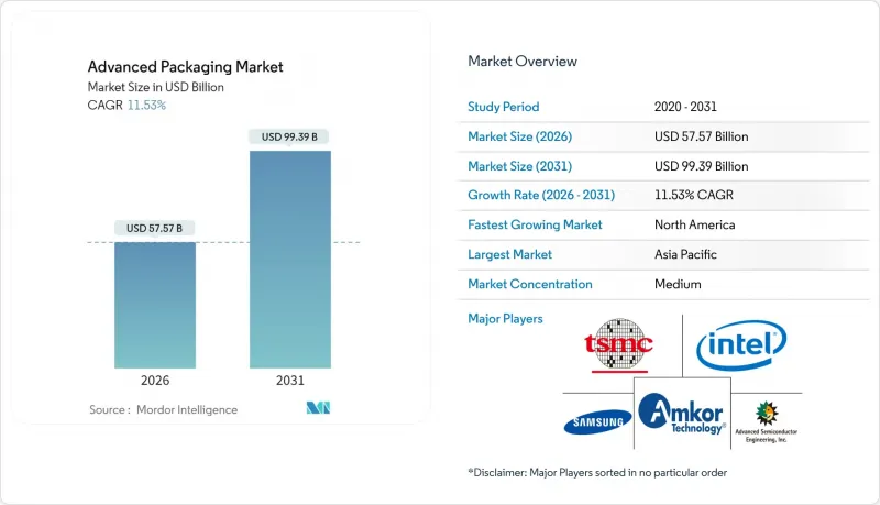
첨단 패키징 시장은 2025년 516억 2,000만 달러에서 2026년에는 575억 7,000만 달러로 성장하여 2026년부터 2031년까지 CAGR 11.53%를 기록하며 2031년까지 993억 9,000만 달러에 달할 것으로 예측됩니다.
기존 패키지의 열적 및 상호연결 한계를 넘어선 인공지능(AI) 프로세서에서 이기종 통합이 필수적이기 때문에 수요는 당초 예상보다 더 많이 증가했습니다. 이에 따라, 통합디바이스 제조업체(IDM)와 아웃소싱 반도체 조립 및 테스트(OSAT) 업체들은 설비투자를 가속화하고, 각국 정부는 조립 능력의 국산화를 위해 대규모 우대 조치를 취했습니다. 첨단 패키징 시장은 유리 코어 기판의 연구 개발, 패널 레벨 가공의 시범 도입, 하이퍼스케일 데이터센터의 광학 부품 공동 실장 기술의 급속한 보급으로 인해 혜택을 받았습니다. 그러나 BT 수지 기판 부족과 엔지니어링 인력 부족으로 인해 적시에 생산능력을 확대하지 못해 공급은 계속 타이트한 상태였습니다. 파운드리가 AI 공급망의 엔드투엔드 관리를 위해 패키징을 내재화하면서 경쟁이 치열해졌고, 기존 OSAT 업체들의 수익률을 압박하는 동시에 전략적 전문화를 촉진했습니다.
세계 첨단 패키징 시장 동향과 인사이트
AI 및 HPC를 위한 이기종 통합에 대한 수요 증가
AI 워크로드는 기존 패키징 기술로는 달성할 수 없는 연산 밀도와 메모리 대역폭을 요구합니다. TSMC의 CoWoS 플랫폼은 칩렛과 고대역폭 메모리를 단일 구조로 통합하여 주요 AI 가속기 벤더들 사이에서 빠르게 채택되고 있습니다. 삼성의 SAINT 기술은 차세대 HBM4 스택에 대응하는 하이브리드 본딩을 통해 동일한 목표를 달성함으로써, 삼성의 첨단 패키징 기술의 전략적 가치를 부각시켰습니다. 열 인터페이스 재료, 특수 기판, 액티브 인터포저의 도입으로 패키지 비용은 전체 반도체 제조 재료비의 15-20%(주류 CPU의 경우 5-8%)로 상승했습니다. 그 결과, AI 시스템의 시장 출시 시기를 결정하는 데 있어 첨단 패키징 생산능력은 첨단 팹과 동등하게 중요해졌습니다. 따라서 첨단 패키징 시장은 전 공정 공정의 전환에 뒤처지지 않고 병행하여 성장하고 있습니다.
가전제품의 소형화로 WLP 채택 촉진
스마트폰, 웨어러블 기기, 히어러블 기기는 항상 얇은 두께와 고기능 밀도를 요구하고 있습니다. 팬아웃 웨이퍼 레벨 패키징(FOWLP)은 0.5mm 미만의 초박형 패키지에 여러 개의 다이를 통합할 수 있어 열 성능 저하 없이 플래그십 모바일 프로세서를 지원할 수 있습니다. 팬인 WLP에서 FOWLP로 전환함으로써 언더필, 와이어 본딩, 적층 기판이 불필요해져 전체 시스템 비용을 최대 25%까지 절감할 수 있습니다. 소형화 추세는 치수가 생명과 직결되는 임베디드 의료용 전자기기 분야로까지 파급되었습니다. 리드스페이스 제조업체는 WLP 기술을 통해 까다로운 신뢰성 목표를 달성하면서 디바이스 크기를 93%까지 줄이는 데 성공했습니다. 그 결과, 민수 및 의료용 수요는 지속적인 기반을 형성하여 PC 엔드 시장의 주기적 변동으로부터 첨단 패키징 시장을 보호하는 역할을 하였습니다.
높은 자본집약도가 시장 진입을 제약하는 요인
2.5D 및 3D 공정용 툴의 비용은 챔버당 1,000만-1,500만 달러에 달해 기존 라인의 일반적인 300만 달러를 크게 상회합니다. TSMC는 2025년에 420억 달러의 설비 투자 예산을 책정했으며, 그 중 상당 부분이 첨단 패키징 확장에 투입됐습니다. 이에 따라 중소 OSAT 기업들은 빠르게 단축되는 제품 수명주기 동안 투자를 상각하는 데 어려움을 겪었고, 틈새 분야로 특화하거나 방어적 합병을 추진하게 되었습니다. 이러한 높은 진입장벽으로 인해 상위권 기업과 후발주자 간의 기술 격차가 확대되고, 2024년부터 2026년까지 첨단 패키징 시장의 신규 설비투자가 억제될 것으로 예상됩니다.
부문 분석
2025년에는 플립칩 패키지가 48.30%의 매출 점유율로 1위를 차지할 것으로 예상되며, 대량 생산되는 민수 및 산업용 애플리케이션이 그 기반이 될 것으로 보입니다. 그러나 AI 가속기가 플립칩의 한계를 뛰어넘는 로직과 메모리 근접성을 요구함에 따라 2.5D/3D 구성이 가장 빠른 성장세를 보이며 13.05%의 CAGR 전망을 달성했습니다. 2.5D/3D 솔루션의 첨단 패키징 시장 규모는 2031년까지 389억 달러에 달할 것으로 예상되며, 플랫폼 총 수익의 39.15%를 차지할 것으로 예측됩니다.
삼성의 SAINT 플랫폼은 10μm 미만의 하이브리드 본딩을 실현하여 와이어 본딩 방식 대비 신호 지연을 30% 감소시키고, 열적 여유를 40% 확대했습니다. TSMC의 CoWoS는 2025년 3개 라인 추가 증설로 12개월치 수주잔고를 해소했습니다. 임베디드 다이와 팬아웃 WLP는 상호 보완적인 선택으로 발전했다: 임베디드 패키지는 공간 제약이 있는 자동차 분야에 적합하고, 팬아웃 WLP는 5G 기지국 및 밀리미터파 레이더 설계에 적합합니다. 이러한 추세와 함께 2.5D/3D 패키징은 차세대 디바이스 로드맵의 중심에 자리 잡으며 첨단 패키징 시장의 주요 가치 동인으로서의 역할을 확고히 하고 있습니다.
2025년 출하량의 39.20%를 차지했지만, 그 성장률은 한 자릿수 성장률에 그쳤습니다. 반면, 자동차 및 전기자동차 수요는 CAGR 12.32%로 확대되어 2031년까지 첨단 패키징 시장 점유율을 18.6%까지 끌어올릴 것으로 예상됩니다. 자동차 전장용 첨단 패키징 시장 규모는 예측 기간이 끝날 때까지 185억 달러가 넘을 것으로 예상됩니다.
EV용 트랙션 인버터, 차량용 충전기, 도메인 컨트롤러는 현재 자동차 등급의 팬아웃형, 양면 냉각 파워 모듈, 오버몰드 방식의 시스템 인 패키지(SiP) 어셈블리를 채택하고 있습니다. 데이터센터 인프라도 고성장 분야 중 하나입니다. AI 서버는 1,000W/cm2에 달하는 전력 밀도를 실현하는 첨단 패키징을 활용하고 있으며, 혁신적인 써멀리드 및 언더필 재료의 개발이 요구되고 있습니다. 한편, 의료 분야에서는 생체적합성 코팅과 밀폐형 인클로저가 요구되고 있으며, 이러한 특성은 높은 가격대의 평균 판매 가격과 안정적인 교체 수요를 가져옵니다. 이러한 부문별 동향이 결합되어 수익원이 다양해지면서 첨단 패키징 시장에서 스마트폰 업데이트 주기에 대한 의존도가 낮아졌습니다.
첨단 패키징 시장은 패키징 플랫폼(플립칩, 임베디드 다이, 팬인 WLP 등), 최종사용자 산업(가전, 자동차 및 EV, 데이터센터 및 HPC 등), 디바이스 아키텍처(2D IC, 2.5D 인터포저, 3D IC), 인터커넥트 기술(솔더 범프, 구리 기둥, 하이브리드 본딩), 지역(북미, 유럽, 아시아태평양, 중동, 일본, 중국, 유럽, 미국, 일본) ), 인터커넥트 기술(솔더 범프, 구리 필러, 하이브리드 본딩), 지역(아메리카, 유럽, 아시아태평양, 중동 및 아프리카)으로 구분됩니다.
지역별 분석
아시아태평양은 2025년 매출의 74.10%를 차지했습니다. 이는 대부분의 프론트엔드 팹 및 기판 공급업체가 대만, 한국, 중국 본토에 위치하고 있기 때문입니다. TSMC는 1,650억 달러의 미국 투자를 발표했지만, 이는 대만 거점을 대체하는 것이 아니라 다각화 전략을 반영한 것으로, 중기적으로 아시아가 주도권을 유지할 수 있도록 보장하는 것입니다. 중국 국내 OSAT(위탁 조립 및 테스트) 업체들은 두 자릿수 매출 증가를 달성하고 자동차 패키징 분야에도 진출했지만, 극자외선(EUV) 장비에 대한 엄격한 규제로 인해 최첨단 웨이퍼 제조 공정에 대한 진입이 제한되고 있습니다.
북미는 CHIPS 법의 특혜로 인해 CAGR 12.38%로 가장 빠르게 성장하는 지역으로 부상했습니다. 20억 달러 규모의 Amkor의 애리조나 공장은 2027년 본격 가동 시 범프, 웨이퍼 레벨, 패널 레벨 라인을 통합하여 미국 시스템 통합업체 인근의 첫 번째 대규모 아웃소싱 기지를 형성할 예정입니다. 인텔, 애플, 엔비디아와 엔비디아는 지정학적 공급 중단 리스크를 줄이기 위해 이 생산능력의 일부를 사전 예약하고, 기존에는 동아시아 OSAT(위탁 조립 및 테스트) 업체로 흘러가던 상당량의 생산량을 전환했습니다. 그 결과, 첨단 패키징 시장에 대량의 AI 제품을 지원할 수 있는 신뢰할 수 있는 북미 공급 기지가 추가되었습니다.
유럽은 대량 생산 중심이 아닌 전문 분야 추구를 선택했습니다. 온세미컨덕터 체코 공장은 자동차용 파워용 탄화규소 소자를 전문으로 생산하며, 현지 OEM의 전동화 목표에 부합하는 생산 체제를 구축했습니다. 독일 프라운호퍼 연구소가 패널 레벨 기술 조사를 주도했지만, 제조사들은 신규 메가사이트에 대한 투자에 신중한 태도를 유지했습니다. 한편, 싱가포르는 허브 기능을 강화했습니다. 마이크로닉스의 HBM 공장과 KLA의 공정 제어 확장을 통해 단일 관할권 내에서 AI 메모리 및 계측 기술을 지원하는 수직 통합형 에코시스템이 구축되었습니다. 인도는 자본비용 50% 분담제도를 도입하고 중기적 성장이 기대되는 선진 패키징 시범사업을 유치했지만, 인력 확보가 과제로 남아있습니다.
이러한 움직임이 결합되어 시스템 OEM 제조업체의 지리적 위험이 분산되고 고급 패키징 시장이 재조정되었습니다. 그럼에도 불구하고 아시아태평양은 2031년에도 60% 이상의 점유율을 유지할 것으로 예상됩니다. 기존 인프라, 공급 클러스터, 규모의 경제가 여전히 신규 진입 지역을 압도하고 있기 때문입니다.
기타 특전:
- 엑셀 형식의 시장 예측(ME) 시트
- 애널리스트의 3개월간 지원
자주 묻는 질문
목차
제1장 소개
제2장 조사 방법
제3장 주요 요약
제4장 시장 구도
제5장 시장 규모와 성장 예측
제6장 경쟁 구도
제7장 시장 기회와 향후 전망
KSM 26.03.09The advanced packaging market is expected to grow from USD 51.62 billion in 2025 to USD 57.57 billion in 2026 and is forecast to reach USD 99.39 billion by 2031 at 11.53% CAGR over 2026-2031.

Demand outpaced earlier projections because heterogeneous integration became indispensable for artificial-intelligence (AI) processors that exceed the thermal and interconnect limits of conventional packages. In response, integrated-device manufacturers (IDMs) and outsourced semiconductor assembly and test (OSAT) providers accelerated capital spending, while governments earmarked large incentives to localize assembly capacity. The advanced packaging market also benefited from glass-core substrate R&D, panel-level processing pilots, and the rapid adoption of co-packaged optics in hyperscale data centers. Supply remained tight, however, as BT-resin substrate shortages and scarce engineering talent hindered timely capacity additions. Competitive intensity rose as foundries internalized packaging to secure end-to-end control of AI supply chains, squeezing traditional OSAT margins and prompting strategic specialization.
Global Advanced Packaging Market Trends and Insights
Rising demand for heterogeneous integration for AI and HPC
AI workloads require compute density and memory bandwidth unattainable with legacy packaging. TSMC's CoWoS platform integrates chiplets and high-bandwidth memory in a single structure, gaining rapid adoption among leading AI accelerator vendors. Samsung's SAINT technology achieved similar objectives using hybrid bonding that supports forthcoming HBM4 stacks, underscoring the strategic value of in-house advanced packaging. Thermal interface materials, specialized substrates, and active interposers raised package cost to 15-20% of the total semiconductor build-to-materials, up from 5-8% for mainstream CPUs. As a result, advanced packaging capacity became as critical as leading-edge fabs in determining time-to-market for AI systems. The advanced packaging market, therefore, grew in tandem with, rather than lagging, front-end process migrations.
Miniaturization of consumer devices boosting WLP adoption
Smartphones, wearables, and hearables consistently demand thinner profiles and higher functional density. Fan-out wafer-level packaging (FOWLP) enables multiple dies to be embedded in ultra-thin packages below 0.5 mm, supporting flagship mobile processors without compromising thermal performance. The shift from fan-in WLP to FOWLP reduced overall system cost by up to 25% because under-fill, wire-bonding, and laminate substrates were eliminated. Miniaturization also moved into implantable medical electronics, where dimensions are life-critical; leadless pacemakers benefited from WLP to cut device size by 93% while meeting stringent reliability targets. Consequently, consumer and medical demand created a recurring baseline that insulated the advanced packaging market from cyclical swings in PC end-markets.
High capital intensity constraining market entry
Tooling for 2.5D and 3D processes can cost USD 10-15 million per chamber, vastly exceeding the USD 3 million typical for legacy lines. TSMC budgeted USD 42 billion in 2025 capital outlays, of which a material share targeted advanced packaging expansions. Smaller OSATs, therefore, struggled to amortize investments across rapidly shrinking product life cycles, prompting niche specialization or defensive mergers. The elevated hurdle rate widened the technological gap between tier-one providers and regional followers, dampening fresh capacity in the advanced packaging market during 2024-2026.
Other drivers and restraints analyzed in the detailed report include:
- Government semiconductor subsidies accelerating infrastructure development
- EV power-electronics reliability transforming packaging requirements
- BT-resin substrate bottlenecks limiting production capacity
For complete list of drivers and restraints, kindly check the Table Of Contents.
Segment Analysis
Flip-chip packages retained leadership with 48.30% revenue in 2025, anchored by high-volume consumer and industrial applications. Yet 2.5D/3D configurations delivered the fastest gains, achieving a 13.05% CAGR outlook as AI accelerators demanded logic-to-memory proximity beyond flip-chip limits. The advanced packaging market size for 2.5D/3D solutions is forecast to reach USD 38.9 billion by 2031, equal to 39.15% of total platform revenue.
Samsung's SAINT platform attained sub-10 µm hybrid bonds, reducing signal latency by 30% and extending thermal headroom by 40% relative to wire-bonded stacks. TSMC's CoWoS ramped three additional lines in 2025 to clear a 12-month backlog. Embedded-die and fan-out WLP progressed as complementary options: embedded packages suited space-constrained automotive domains, while fan-out WLP captured 5G base-station and mmWave radar designs. Collectively, these dynamics embedded 2.5D/3D packaging at the center of next-generation device roadmaps, guaranteeing its role as the prime value driver inside the advanced packaging market.
Consumer electronics absorbed 39.20% of 2025 shipments, but its growth plateaued at single digits. In contrast, automotive and EV demand is projected to expand at a 12.32% CAGR, lifting its share of the advanced packaging market to 18.6% by 2031. The advanced packaging market size for automotive electronics is estimated to surpass USD 18.5 billion by the end of the forecast period.
EV traction inverters, on-board chargers, and domain controllers now specify automotive-grade fan-out, double-side cooled power modules, and over-molded system-in-package (SiP) assemblies. Data-center infrastructure provided another high-growth niche: AI servers utilize advanced packages with power densities reaching 1,000 W/cm2, dictating innovative thermal lid and under-fill chemistries. Healthcare, meanwhile, requires biocompatible coatings and hermetic enclosures, attributes that carry premium average selling prices and stable replacement demand. Cumulatively, these segment trends diversified revenue streams and reduced dependence on cyclical smartphone refresh cycles within the advanced packaging market.
Advanced Packaging Market is Segmented by Packaging Platform (Flip-Chip, Embedded Die, Fan-In WLP, and More), End-User Industry (Consumer Electronics, Automotive and EV, Data Center and HPC, and More), Device Architecture (2D IC, 2. 5D Interposer, and 3D IC), Interconnect Technology (Solder Bump, Copper Pillar, and Hybrid Bond), and Geography (North America, South America, Europe, Asia-Pacific, and Middle East and Africa).
Geography Analysis
Asia-Pacific generated 74.10% of 2025 revenue because Taiwan, South Korea, and mainland China house the bulk of front-end fabs and substrate suppliers. TSMC announced a USD 165 billion U.S. investment, reflecting a diversification strategy rather than the displacement of its Taiwan base, ensuring Asia retains leadership in the medium term. China's domestic OSATs delivered double-digit sales gains and expanded into automotive packaging, but tight controls on extreme-ultraviolet (EUV) tools limited their move into leading-edge wafer-fab processes.
North America emerged as the fastest-growing region at a 12.38% CAGR thanks to the CHIPS Act incentives. Amkor's USD 2 billion Arizona site will combine bump, wafer-level, and panel-level lines once fully ramped in 2027, providing the first large-scale outsourced option near U.S. system integrators. Intel, Apple, and NVIDIA pre-booked a portion of this capacity to de-risk geopolitical supply interruptions, redirecting meaningful volumes that historically flowed to East Asian OSATs. Consequently, the advanced packaging market now includes a credible North American supply node capable of high-volume AI product support.
Europe pursued specialization rather than volume leadership. onsemi's Czech facility addressed silicon-carbide devices for automotive power, aligning with local OEM electrification targets. Germany's Fraunhofer institutes led panel-level research, but manufacturers stayed cautious on green-field megasite commitments. Meanwhile, Singapore strengthened its hub role; Micron's HBM plant and KLA's process-control expansion created a vertically coherent ecosystem that supports AI memory and metrology under one jurisdiction. India introduced a 50% capital cost-sharing scheme, attracting proposals for advanced packaging pilots that promise medium-term upside yet remain contingent on talent availability.
Collectively, these developments diversified geographic risk for system OEMs and rebalanced the advanced packaging market. Even so, Asia-Pacific is forecast to maintain more than 60% share in 2031 because existing infrastructure, supply clusters, and economies of scale still surpass new regional entrants.
- Amkor Technology, Inc.
- Taiwan Semiconductor Manufacturing Company Limited
- Advanced Semiconductor Engineering, Inc.
- JCET Group Co., Ltd.
- Samsung Electronics Co., Ltd.
- Intel Corporation
- Chipbond Technology Corporation
- ChipMOS Technologies Inc.
- Powertech Technology Inc.
- TongFu Microelectronics Co., Ltd.
- Nepes Corporation
- STATS ChipPAC Pte. Ltd.
- Siliconware Precision Industries Co., Ltd.
- UTAC Holdings Ltd.
- Walton Advanced Engineering, Inc.
- Xintec Inc.
- Tianshui Huatian Technology Co., Ltd.
- King Yuan Electronics Co., Ltd.
- Signetics Corporation
- GlobalFoundries Inc.
- Semiconductor Manufacturing International Corporation
- SFA Semicon Co., Ltd.
- Nantong Fujitsu Microelectronics Co., Ltd.
- Hana Micron Inc.
- Unisem (M) Berhad
Additional Benefits:
- The market estimate (ME) sheet in Excel format
- 3 months of analyst support
TABLE OF CONTENTS
1 INTRODUCTION
- 1.1 Study Assumptions and Market Definition
- 1.2 Scope of the Study
2 RESEARCH METHODOLOGY
3 EXECUTIVE SUMMARY
4 MARKET LANDSCAPE
- 4.1 Market Overview
- 4.2 Impact of Macroeconomic Factors
- 4.3 Market Drivers
- 4.3.1 Rising demand for heterogeneous integration for AI and HPC
- 4.3.2 Miniaturization of consumer devices boosting WLP adoption
- 4.3.3 Government semiconductor subsidies (e.g., CHIPS, EU Chips Act)
- 4.3.4 EV power-electronics reliability needs (advanced power packages)
- 4.3.5 Emerging glass-core substrates enabling panel-level packaging
- 4.3.6 Co-packaged optics demand in hyperscale datacenters
- 4.4 Market Restraints
- 4.4.1 High capital intensity of advanced packaging lines
- 4.4.2 Industry consolidation squeezing outsourced margins
- 4.4.3 BT-resin substrate capacity bottlenecks
- 4.4.4 Shortage of advanced assembly talent
- 4.5 Value Chain Analysis
- 4.6 Regulatory Landscape
- 4.7 Technological Outlook
- 4.8 Porter's Five Forces Analysis
- 4.8.1 Threat of New Entrants
- 4.8.2 Bargaining Power of Buyers
- 4.8.3 Bargaining Power of Suppliers
- 4.8.4 Threat of Substitutes
- 4.8.5 Intensity of Rivalry
- 4.9 Investment Analysis
5 MARKET SIZE AND GROWTH FORECASTS (VALUE)
- 5.1 By Packaging Platform
- 5.1.1 Flip-Chip
- 5.1.2 Embedded Die
- 5.1.3 Fan-in WLP
- 5.1.4 Fan-out WLP
- 5.1.5 2.5D / 3D
- 5.2 By End-User Industry
- 5.2.1 Consumer Electronics
- 5.2.2 Automotive and EV
- 5.2.3 Data Center and HPC
- 5.2.4 Industrial and IoT
- 5.2.5 Healthcare / Med-tech
- 5.3 By Device Architecture
- 5.3.1 2D IC
- 5.3.2 2.5D Interposer
- 5.3.3 3D IC (TSV / Hybrid-Bond)
- 5.4 By Interconnect Technology
- 5.4.1 Solder Bump
- 5.4.2 Copper Pillar
- 5.4.3 Hybrid Bond
- 5.5 By Geography
- 5.5.1 North America
- 5.5.1.1 United States
- 5.5.1.2 Canada
- 5.5.1.3 Mexico
- 5.5.2 South America
- 5.5.2.1 Brazil
- 5.5.2.2 Argentina
- 5.5.2.3 Rest of South America
- 5.5.3 Europe
- 5.5.3.1 Germany
- 5.5.3.2 France
- 5.5.3.3 United Kingdom
- 5.5.3.4 Italy
- 5.5.3.5 Netherlands
- 5.5.3.6 Russia
- 5.5.3.7 Rest of Europe
- 5.5.4 Asia-Pacific
- 5.5.4.1 China
- 5.5.4.2 Taiwan
- 5.5.4.3 South Korea
- 5.5.4.4 Japan
- 5.5.4.5 Singapore
- 5.5.4.6 Malaysia
- 5.5.4.7 India
- 5.5.4.8 Rest of Asia-Pacific
- 5.5.5 Middle East and Africa
- 5.5.5.1 Middle East
- 5.5.5.1.1 Israel
- 5.5.5.1.2 United Arab Emirates
- 5.5.5.1.3 Saudi Arabia
- 5.5.5.1.4 Turkey
- 5.5.5.1.5 Rest of Middle East
- 5.5.5.2 Africa
- 5.5.5.2.1 South Africa
- 5.5.5.2.2 Nigeria
- 5.5.5.2.3 Rest of Africa
- 5.5.5.1 Middle East
- 5.5.1 North America
6 COMPETITIVE LANDSCAPE
- 6.1 Market Concentration
- 6.2 Strategic Moves
- 6.3 Market Share Analysis
- 6.4 Company Profiles (includes Global level Overview, Market level overview, Core Segments, Financials as available, Strategic Information, Market Rank/Share for key companies, Products and Services, and Recent Developments)
- 6.4.1 Amkor Technology, Inc.
- 6.4.2 Taiwan Semiconductor Manufacturing Company Limited
- 6.4.3 Advanced Semiconductor Engineering, Inc.
- 6.4.4 JCET Group Co., Ltd.
- 6.4.5 Samsung Electronics Co., Ltd.
- 6.4.6 Intel Corporation
- 6.4.7 Chipbond Technology Corporation
- 6.4.8 ChipMOS Technologies Inc.
- 6.4.9 Powertech Technology Inc.
- 6.4.10 TongFu Microelectronics Co., Ltd.
- 6.4.11 Nepes Corporation
- 6.4.12 STATS ChipPAC Pte. Ltd.
- 6.4.13 Siliconware Precision Industries Co., Ltd.
- 6.4.14 UTAC Holdings Ltd.
- 6.4.15 Walton Advanced Engineering, Inc.
- 6.4.16 Xintec Inc.
- 6.4.17 Tianshui Huatian Technology Co., Ltd.
- 6.4.18 King Yuan Electronics Co., Ltd.
- 6.4.19 Signetics Corporation
- 6.4.20 GlobalFoundries Inc.
- 6.4.21 Semiconductor Manufacturing International Corporation
- 6.4.22 SFA Semicon Co., Ltd.
- 6.4.23 Nantong Fujitsu Microelectronics Co., Ltd.
- 6.4.24 Hana Micron Inc.
- 6.4.25 Unisem (M) Berhad
7 MARKET OPPORTUNITIES AND FUTURE OUTLOOK
- 7.1 White-space and Unmet-Need Assessment
