
|
시장보고서
상품코드
2044014
AI 및 HPC 반도체 실리콘 웨이퍼 : 시장 점유율 분석, 업계 동향 및 통계, 성장 예측(2026-2031년)AI And HPC Semiconductor Silicon Wafer - Market Share Analysis, Industry Trends & Statistics, Growth Forecasts (2026 - 2031) |
||||||
AI 및 HPC 반도체 실리콘 웨이퍼 시장 규모는 2025년 29억 평방인치로 평가되었습니다. 2026년 34억 1,000만 평방인치로부터, 2031년까지 81억 1,000만 평방인치로 확대되며 2026년부터 2031년까지 연평균 복합 성장률(CAGR)은 18.94%를 나타낼 전망입니다.

3나노미터 이하 로직에 대한 생산 능력 확보, 정부 보조금 프로그램과 연계된 다년 계약, 추론에 최적화된 가속기로의 전환이 결합되어 수요의 모멘텀을 촉진하고 있습니다. 대만, 한국, 미국, 중국에서는 300mm 라인의 증설이 결정 인출 장치의 납품 속도를 뛰어넘는 속도로 진행되고 있으며, 현물 시장공급 부족을 초래하여 계약 가격을 끌어올리고 있습니다. 워싱턴, 브뤼셀, 베이징의 병행 보조금 제도로 인해 지리적으로 균형 잡힌 투자가 촉진되어 아시아 파운드리는 더 이상 유럽과 미국의 동종업계가 시장에서 퇴출되지 않습니다. 이러한 요인을 종합하면, 평탄도 및 결함 밀도 측면에서 업계를 선도하는 웨이퍼 공급업체는 향후 10년간 구조적으로 높은 수익률을 달성할 수 있는 위치에 있습니다.
세계의 AI 및 HPC 반도체 실리콘 웨이퍼 시장 동향과 인사이트
AI 가속기용 300mm 웨이퍼 수요 급증
하이퍼스케일 사업자들은 2025년에 1,200만 개의 가속기 카드를 구매했으며, 각 유닛은 300mm 기판에서 최대 1,200mm2의 실리콘을 소비하며, 범용 CPU보다 40% 더 큰 실적를 차지합니다. 칩-온-웨이퍼-온-서브스트레이트(CoWS) 패키징은 리트리클 제약이 있는 여러 다이가 하나의 인터포저를 공유하기 때문에 GPU당 웨이퍼 사용량이 두 배로 증가합니다. 마이크로소프트와 메타가 2026년 자체 3나노미터 추론 프로세서를 출시할 계획은 수요 압력을 더욱 높이고 있습니다. 최첨단 로직용 200mm 기판의 경제적 노후화로 인해 총 두께 편차를 0.15µm 이하로 억제할 수 있는 300mm 라인에 생산량이 집중되고 있습니다. 현재 이 공차를 충족하는 세계 공급업체는 5개 미만이며, 이는 예측 기간 동안 과점적 가격 결정력을 유지하게 될 것입니다.
대만과 미국 내 7nm 이하 파운드리의 급속한 확장
TSMC는 2025년 12월 4나노미터 엔지니어링 웨이퍼 출하를 시작한 애리조나 공장에 650억 달러를 투자했습니다. Samsung Electronics 평택캠퍼스에는 2026년 중반 양산 예정인 2나노미터 GaAA(Gate All Around) 소자를 위한 5번째 클린룸이 추가됐습니다. 인텔의 오하이오주 프로젝트는 2027년 18A 공정으로월6만 장의 웨이퍼 생산 능력을 갖출 것으로 예측됩니다. 이 세 가지 프로젝트만으로 2028년까지월30만 장의 생산능력이 추가되지만, 설비 병목현상으로 인해 본격적인 생산 시작은 12-18개월 정도 늦어질 것으로 예측됩니다. 따라서 7나노미터 이하 생산능력에서 대만의 점유율은 2023년 92%에서 2027년 약 78%로 감소할 것으로 예측됩니다. 이로 인해 지정학적 리스크는 분산되지만, 관할권별 수출 규제에 따른 마찰이 발생하여 국경을 넘는 물류가 복잡해집니다.
초순수 폴리실리콘 공급망의 취약성
2025년에는 7개 기업이 반도체용 폴리실리콘의 거의 전량을 생산했고, 그중 와커, 헴록, 토쿠야마의 3개 기업이 65%를 차지했습니다. 태양광 발전 수요로 인해 그해 현물 가격은 1kg당 28달러에서 41달러로 상승했습니다. 미국의 강제 노동 규제로 인해 신강산이 배제되어 4만 톤의 생산 능력을 잃었습니다. 토카야마의 사라왁 확장으로 2026년 중반에 1만 톤이 추가될 예정이지만, 18개월의 인증 기간이 필요합니다. 따라서 장기 계약이 없는 중소 웨이퍼 제조업체는 원자재 배급제에 직면하고 있으며, 이것이 완화되지 않으면 예측 CAGR을 2퍼센트 포인트 가까이 떨어뜨릴 수 있습니다.
부문 분석
AI 및 HPC 반도체 실리콘 웨이퍼 시장에서 300mm 부문은 2025년 시장 점유율의 94.64%를 차지했으며, 이는 우수한 다이 수율로 인한 경제성을 반영합니다. 300mm 디스크 1장당 유효면적은 200mm 기판의 약 2.4배로 트랜지스터 1개당 제조비용을 30-40% 절감할 수 있습니다. TSMC의 CoWoS와 같은 파운드리 패키징 흐름은 300mm 인터포저만 지원하므로, 하이퍼스케일 기업들은 이 직경에 얽매이게 됩니다. 인텔이 도입 예정인 백사이드 파워 아키텍처는 총 두께 허용범위가 0.12µm으로 엄격해져 기존 200mm 제조 장비로는 달성할 수 없는 수치입니다. 그 결과, 초평탄 300mm 결정체 제조 기술을 습득한 공급업체는 모든 첨단 로직 팹에서 우선 공급업체로 자리매김하고 있습니다.
하이퍼스케일러 업체들이 2026년 이후 3나노미터 노드에서 맞춤형 추론 칩 생산을 계획하고 있는 만큼, 이러한 성장세가 꺾일 가능성은 거의 없을 것으로 보입니다. 따라서 이 부문의 CAGR 19.68%는 평방인치 단위로 측정된 AI 및 HPC 반도체 실리콘 웨이퍼 시장의 전체 규모 추이를 상회하는 것으로 나타났습니다. 한편, 다이 사이즈가 여전히 작은 FD-SOI와 탄화규소(SiC) 용도에 힘입어 200mm 웨이퍼 수요는 꾸준히 증가하고 있습니다. 장비 업체들은 150mm 서비스 제공을 중단하기 시작했고, 이로 인해 구식 팹은 전환하거나 철수해야 하는 상황에 처해 있으며, 이러한 추세는 업계 구조조정을 가속화하고 있습니다. GlobalWafers의 Siltronic 싱가포르 자산 인수 등 최근 M&A를 통해 중국 외 300mm 생산능력의 4분의 1 이상이 단일 소유주 아래 통합되어 파운드리 고객과의 협상 역학이 재편되고 있습니다.
'AI 및 HPC 반도체 실리콘 웨이퍼 시장 보고서'는 웨이퍼 직경(300mm 및 200mm), 기술 노드(고급 노드, 메인스트림 노드, 성숙 노드), 지역별로 분류되어 있습니다. 시장 예측은 수량(평방인치) 단위로 제공됩니다.
지역별 분석
아시아태평양은 2025년 시장 점유율의 74.62%를 차지했으며, 2031년까지 연평균 19.82%의 성장률을 나타낼 것으로 전망됩니다. TSMC는 대만 전역에서 월 80만 장의 웨이퍼를 소비하고 있으며, 2026년 하반기에는 일본 구마모토의 신공장이 5만 5,000장을 추가할 것으로 예측됩니다. 삼성 평산(평택) 캠퍼스는 2025년 P4 라인이 가동된 후 월 40만 장의 생산량을 달성했습니다. 중국은 2025년까지 국내 웨이퍼 조달률을 32%까지 끌어올려 결함 밀도 격차에도 불구하고 수입품을 대체하고, 업스트림 재료에 1,500억 위안을 투입했습니다. 일본은 대만에 대한 집중을 피하기 위해 4조 엔(270억 달러)의 보조금을 확보하여 숙련된 노동력을 둘러싼 지역 간 경쟁을 심화시키고 있습니다.
북미는 규모는 작지만 'CHIPS법'의 인센티브에 따라 빠르게 성장하고 있습니다. 인텔의 애리조나 주와 오하이오 주에 위치한 인텔 공장은 2028년까지 월 12만 장을 생산할 것으로 예상되며, TSMC의 피닉스 공장에서는 이미 4나노미터 실리콘이 출하되고 있습니다. 세계 웨이퍼는 텍사스 주 셔먼에 50억 달러를 투자해 연간 120만 장의 웨이퍼 생산을 목표로 하는 공장 착공에 들어갔습니다. 물 부족이 제약 요인으로 떠오르고 있으며, 애리조나 주 팹은 하루에 400만 갤런의 물을 소비하기 때문에 규제 당국은 90%의 재사용 목표를 요구하고 있지만, 현재 TSMC만이 이를 달성하고 있습니다. 지속 가능한 물 사용 효율의 달성은 향후 인센티브 지급에 있어 중요한 조건이 되고 있습니다.
2025년 유럽은 전 세계 반도체 생산량(평방인치 기준)의 8%를 차지했으며, 자동차 및 파워 디바이스에 특화되어 있습니다. 인피니언의 드레스덴 공장과 ST마이크로일렉트로닉스의 크롤 공장은 칩스법(Chips Act)의 현지 조달 요건을 충족하기 위해 실트로닉의 프라이베르크 공장에서 웨이퍼를 조달하고 있습니다. 보쉬는 차량용 센서 부족을 완화하기 위해 로이틀링겐에 200mm 라인을 추가했지만, 최첨단 로직은 여전히 수입에 의존하고 있습니다. 남미, 중동, 아프리카를 합쳐도 생산량의 2% 미만에 불과하고, 프라임 웨이퍼 제조 시설도 존재하지 않기 때문에 아시아태평양의 물류가 타이트해지면 현지 조립업체들이 운송 및 관세 급변에 따른 영향을 받기 쉽습니다.
기타 혜택 :
- 엑셀 형식 시장 예측(ME) 시트
- 3개월간 애널리스트 지원
자주 묻는 질문
목차
제1장 서론
제2장 조사 방법
제3장 주요 요약
제4장 시장 구도
제5장 시장 규모와 성장 예측
제6장 경쟁 구도
제7장 시장 기회와 향후 전망
KTH 26.05.29The AI and HPC semiconductor silicon wafer market size is projected to expand from 2.9 billion square inches in 2025 and 3.41 billion square inches in 2026 to 8.11 billion square inches by 2031, registering a CAGR of 18.94% between 2026 to 2031.
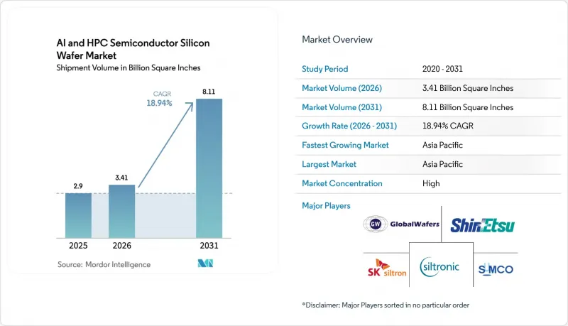
Capacity secured for sub-3-nanometer logic, multi-year offtake deals tied to sovereign subsidy programs, and the migration toward inference-optimized accelerators collectively reinforce demand momentum. Taiwan, South Korea, the United States, and China are expanding 300 millimeter lines faster than crystal-pulling equipment can be delivered, tightening spot availability and lifting contract prices. Asian foundries no longer crowd out Western peers, because parallel subsidy corridors in Washington, Brussels, and Beijing have seeded geographically balanced investments. Taken together, these factors position wafer suppliers with flatness and defect-density leadership to capture structurally higher margins through the decade.
Global AI And HPC Semiconductor Silicon Wafer Market Trends and Insights
Surging Demand for 300mm Wafers in AI Accelerators
Hyperscale operators purchased 1.2 million accelerator cards in 2025, with each unit consuming up to 1,200 mm2 of silicon on 300 millimeter substrates, a footprint 40% larger than general-purpose CPUs. Chip-on-wafer-on-substrate packaging doubles wafer usage per GPU because multiple reticle-limited dies share a single interposer. Transition plans by Microsoft and Meta to launch proprietary 3 nanometer inference processors in 2026 further lift demand pressure. The economic obsolescence of 200 millimeter substrates for leading-edge logic concentrates volume on 300 millimeter lines that can hold total-thickness variation below 0.15 µm. Fewer than five global suppliers currently meet that tolerance, which preserves oligopolistic pricing power through the forecast horizon.
Rapid Foundry Expansions Below 7nm in Taiwan and the United States
TSMC committed USD 65 billion to Arizona plants that began shipping 4 nanometer engineering wafers in December 2025. Samsung's Pyeongtaek campus added a fifth cleanroom for 2 nanometer gate-all-around devices slated for mid-2026 volume. Intel's Ohio project will reach 60,000 wafer starts per month on 18A in 2027. These three programs alone add 300,000 starts monthly by 2028, though equipment bottlenecks push full output 12-18 months to the right. Taiwan's share of sub-7 nanometer capacity therefore declines from 92% in 2023 to roughly 78% in 2027, diffusing geopolitical risk but introducing jurisdictional export-control frictions that complicate cross-border logistics.
Supply Chain Fragility for Ultrapure Polysilicon
Seven firms produced nearly all semiconductor-grade polysilicon in 2025, with Wacker, Hemlock, and Tokuyama covering 65%. Solar demand lifted spot prices from USD 28/kg to USD 41/kg during the year. U.S. forced-labor rules blocked Xinjiang origin, removing 40,000 t of capacity. Tokuyama's Sarawak expansion adds 10,000 t in mid-2026 but needs 18 months of qualification. Smaller wafer houses without long contracts therefore face feedstock rationing, which could shave nearly 2 percentage points off the forecast CAGR if unmitigated.
Other drivers and restraints analyzed in the detailed report include:
- Growing Capital Support for Domestic Wafer Fabs in China
- Aggressive Node Shrinks for Advanced HPC GPUs
- Long Lead Times on Crystal-Pulling Equipment
For complete list of drivers and restraints, kindly check the Table Of Contents.
Segment Analysis
The 300 mm segment of the AI and HPC semiconductor silicon wafer market accounted for 94.64% of the market share in 2025, reflecting its superior die-yield economics. Every 300 millimeter disk offers roughly 2.4X usable area versus a 200 millimeter substrate, reducing manufacturing expense per transistor by 30-40%. Foundry packaging flows, such as TSMC CoWoS, only accept 300 millimeter interposers, which lock hyperscale buyers into this diameter. Intel's upcoming backside power architecture tightens total-thickness budgets to 0.12 µm, a figure unreachable on legacy 200 millimeter tools. Consequently, suppliers that master ultra-flat 300 millimeter crystals hold preferred-vendor status at all advanced logic fabs.
Growth momentum is unlikely to abate, as hyperscalers plan to produce custom inference chips on 3-nanometer nodes from 2026 onward. The segment's 19.68% CAGR, therefore, exceeds the broader AI and HPC semiconductor silicon wafer market size trajectory as measured in square inches. Conversely, demand for 200 millimeter wafers is growing steadily, driven by FD-SOI and silicon-carbide applications where die sizes remain small. Equipment vendors have begun to sunset 150 millimeter service, forcing older fabs either to migrate or exit, a trend that accelerates consolidation. Recent M&A, such as GlobalWafers acquiring Siltronic's Singapore asset, places more than one-quarter of non-Chinese 300 millimeter capacity under one owner, reshaping bargaining dynamics with foundry customers.
The AI and HPC Semiconductor Silicon Wafer Market Report is Segmented by Wafer Diameter (300mm and 200mm), Technology Node (Advanced Node, Mainstream Node, and Mature Node), and Geography. The Market Forecasts are Provided in Terms of Volume (Square Inches).
Geography Analysis
Asia-Pacific retained 74.62% of the market share in 2025 and is forecast to advance at 19.82% through 2031. TSMC alone consumed 800,000 starts per month across Taiwan, while its new Kumamoto plant in Japan adds 55,000 starts in late 2026. Samsung's Pyeongtaek campus reached 400,000 starts monthly after the P4 line came online in 2025. China lifted domestic wafer sourcing to 32% by 2025, substituting imports despite defect-density disparities, and poured RMB 150 billion into upstream materials. Japan attracted JPY 4 trillion (USD 27 billion) in subsidies that hedge against Taiwan concentration, raising regional competition for skilled labor.
North America, though smaller, expands rapidly under CHIPS Act incentives. Intel's Arizona and Ohio sites will draw 120,000 starts monthly by 2028, while TSMC's Phoenix module already ships 4 nanometer silicon. GlobalWafers broke ground on a USD 5 billion Sherman, Texas plant, aiming for 1.2 million wafers annually. Water scarcity surfaced as a binding constraint, with Arizona fabs consuming 4 million gallons daily, prompting regulators to mandate 90% reuse targets that only TSMC currently meets. Achieving sustainable water intensity is now a gating factor for future incentive disbursements.
Europe captured 8% of global square-inch output in 2025, specializing in automotive and power devices. Infineon's Dresden fab and STMicroelectronics' Crolles site pull wafers from Siltronic's Freiberg plant to satisfy Chips Act local-content rules. Bosch added a 200 millimeter line in Reutlingen to ease vehicle-sensor shortages but remains reliant on imports for leading-edge logic. South America and the Middle East and Africa together account for less than 2% of volume and host no prime-wafer facilities, exposing local assemblers to shipping and tariff shocks when Asia-Pacific logistics tighten.
- Shin-Etsu Chemical Co., Ltd.
- Sumco Corporation
- GlobalWafers Co., Ltd.
- Siltronic AG
- SK Siltron Co., Ltd.
- Wafer Works Corporation
- Soitec S.A.
- Okmetic Oyj
- Sil'tronix Silicon Technologies
- Shanghai Simgui Technology Co., Ltd.
- Zhejiang Jinruihong Silicon Material Co., Ltd.
- Episil-Precision Inc.
- Poshing Technology Co., Ltd.
- Heraeus Holding GmbH
- LG Siltron Inc.
- Tokuyama Corporation
- Ferrotec Holdings Corporation
- AXT, Inc.
Additional Benefits:
- The market estimate (ME) sheet in Excel format
- 3 months of analyst support
TABLE OF CONTENTS
1 INTRODUCTION
- 1.1 Study Assumptions and Market Definition
- 1.2 Scope of the Study
2 RESEARCH METHODOLOGY
3 EXECUTIVE SUMMARY
4 MARKET LANDSCAPE
- 4.1 Market Overview
- 4.2 Market Drivers
- 4.2.1 Surging Demand for 300 Mm Wafers in AI Accelerators
- 4.2.2 Rapid Foundry Expansions Below 7 Nm in Taiwan and the United States
- 4.2.3 Growing Capital Support for Domestic Wafer Fabs in China
- 4.2.4 Aggressive Node Shrinks for Advanced HPC GPUs
- 4.2.5 Adoption of Backside-Power Delivery and Wafer-Level Bonding
- 4.2.6 Sustainability Mandates Driving Prime Wafer Recycling
- 4.3 Market Restraints
- 4.3.1 Supply Chain Fragility for Ultrapure Polysilicon
- 4.3.2 Long Lead Times on Crystal-Pulling Equipment
- 4.3.3 High Capex Intensity Limiting New Entrants
- 4.3.4 Water and Power Scarcity Risks at Mega-Fabs
- 4.4 Industry Supply-Chain Analysis
- 4.5 Regulatory Landscape
- 4.6 Technological Outlook
- 4.7 Impact of Macroeconomic Factors on the Market
- 4.8 Porter's Five Forces Analysis
- 4.8.1 Threat of New Entrants
- 4.8.2 Bargaining Power of Suppliers
- 4.8.3 Bargaining Power of Buyers
- 4.8.4 Threat of Substitutes
- 4.8.5 Intensity of Competitive Rivalry
5 MARKET SIZE AND GROWTH FORECASTS (VOLUME)
- 5.1 By Wafer Diameter
- 5.1.1 300 mm
- 5.1.2 200 mm
- 5.2 By Technology Node
- 5.2.1 Advanced Node (Below 7nm)
- 5.2.2 Mainstream Node (10nm-28nm)
- 5.2.3 Mature Node (Above 28nm)
- 5.3 By Geography
- 5.3.1 North America
- 5.3.1.1 United States
- 5.3.1.2 Canada
- 5.3.1.3 Mexico
- 5.3.2 Europe
- 5.3.2.1 Germany
- 5.3.2.2 United Kingdom
- 5.3.2.3 France
- 5.3.2.4 Rest of Europe
- 5.3.3 Asia-Pacific
- 5.3.3.1 China
- 5.3.3.2 Japan
- 5.3.3.3 India
- 5.3.3.4 South Korea
- 5.3.3.5 Taiwan
- 5.3.3.6 Rest of Asia-Pacific
- 5.3.4 South America
- 5.3.5 Middle East and Africa
- 5.3.1 North America
6 COMPETITIVE LANDSCAPE
- 6.1 Market Concentration
- 6.2 Strategic Moves
- 6.3 Market Share Analysis
- 6.4 Company Profiles (includes Global level Overview, Market Level Overview, Core Segments, Financials as Available, Strategic Information, Market Rank/Share for Key Companies, Products and Services, and Recent Developments)
- 6.4.1 Shin-Etsu Chemical Co., Ltd.
- 6.4.2 Sumco Corporation
- 6.4.3 GlobalWafers Co., Ltd.
- 6.4.4 Siltronic AG
- 6.4.5 SK Siltron Co., Ltd.
- 6.4.6 Wafer Works Corporation
- 6.4.7 Soitec S.A.
- 6.4.8 Okmetic Oyj
- 6.4.9 Sil'tronix Silicon Technologies
- 6.4.10 Shanghai Simgui Technology Co., Ltd.
- 6.4.11 Zhejiang Jinruihong Silicon Material Co., Ltd.
- 6.4.12 Episil-Precision Inc.
- 6.4.13 Poshing Technology Co., Ltd.
- 6.4.14 Heraeus Holding GmbH
- 6.4.15 LG Siltron Inc.
- 6.4.16 Tokuyama Corporation
- 6.4.17 Ferrotec Holdings Corporation
- 6.4.18 AXT, Inc.
7 MARKET OPPORTUNITIES AND FUTURE OUTLOOK
- 7.1 White-Space and Unmet-Need Assessment

