

|
시장보고서
상품코드
2065434
GPU 및 HPC 실리콘 인터포저 : 시장 점유율 분석, 업계 동향 및 통계, 성장 예측(2026-2031년)GPU And HPC Silicon Interposer - Market Share Analysis, Industry Trends & Statistics, Growth Forecasts (2026 - 2031) |
||||||
 Mordor Intelligence
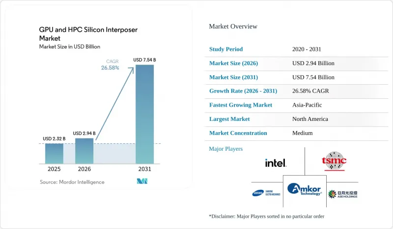
GPU 및 HPC 실리콘 인터포저 시장 규모는 2025년 23억 2,000만 달러로 평가되었습니다. 2026년에는 29억 4,000만 달러로 확대되어 2031년까지 75억 4,000만 달러에 이를 것으로 예상되며 2026년부터 2031년에 걸쳐 CAGR 26.58%로 성장할 전망입니다.
본 보고서는 인터포저의 유형(패시브 실리콘 인터포저 및 액티브 실리콘 인터포저), 용도(AI/머신러닝 가속기, HPC, 데이터센터용 GPU, 네트워크 및 고속 연산), 최종 사용자(클라우드 서비스 제공업체, 연구·정부계 HPC 센터, 기업 데이터센터), 그리고 지역별로 분류되어 있습니다. 시장 전망은 금액(달러) 기준으로 제시되어 있습니다.
세계의 GPU 및 HPC 실리콘 인터포저 시장 동향 및 인사이트
생성형 AI 워크로드의 급속한 확대
최첨단 모델은 현재 1조 개의 파라미터를 초과하며, 20 TB/s를 넘는 메모리 대역폭을 필요로 하지만, 이러한 임계값은 대면적 실리콘 인터포저를 통해서만 달성할 수 있습니다. NVIDIA의 Blackwell 아키텍처는 2026년에 양산이 시작되며, 8개의 HBM3E 스택을 통해 18 TB/s를 구현하기 때문에 패키지 면적은 3,500 mm²를 초과하게 됩니다. 훈련 중심에서 추론 중심으로의 전환에 따라, 2025년에 출시된 마이크로소프트의 Maia 100이나 구글의 TPU v5p에서 볼 수 있듯이, 순수한 연산 밀도보다 메모리 용량과 지연 시간이 우선시되고 있습니다. 각 하이퍼스케일러 기업의 맞춤형 반도체는 GPU 및 HPC 실리콘 인터포저 시장을 세분화하고 있습니다. 이는 각 전용 가속기가 고유한 CoWoS 할당을 필요로 하기 때문에 설령 GPU 유닛의 성장세가 둔화되더라도 수요는 높은 수준을 유지하기 때문입니다. 그 결과, 인터포저 공급업체는 향후 수년간 수요 전망을 확보할 수 있지만, 소량 주문형 설계에 대응해야 하기 때문에 생산 라인 가동률 관리가 복잡해지고 있습니다.
GPU 패키지당 HBM 스택 수 증가
HBM 통합 스택 수는 2022년 4스택에서 2025년에는 8스택으로 두 배로 증가했으며, 2028년에는 12스택으로 확대한다는 로드맵이 순조롭게 진행되고 있습니다. 스택이 하나 늘어날 때마다 TSV 밀도가 두 배로 증가하며, 다이 전체에 걸친 온도 구배가 확대되어 2,000 mm²를 초과합니다. 2024년에 도입된 TSMC의 CoWoS-L은 로직 영역과 메모리 영역을 분리함으로써, 400W의 열 부하 한도를 초과하지 않으면서 12스택 레이아웃을 구현하고 있습니다. 한편, SK하이닉스는 2025년에 12층 적층형 HBM3E의 양산 출하를 시작했습니다. 메모리 분야의 병목 현상은 여전히 심각하며, 3개 업체가 HBM 생산 능력의 95%를 계속 차지하고 있어 인터포저 웨이퍼 계획까지 파급되는 영향이 발생하고 있습니다.
65 K mm² 이상의 인터포저에 대한 파운드리 생산 능력 부족
현재 레티클 크기가 6만 5,000 mm²를 초과하는 인터포저를 제조할 수 있는 공급업체는 TSMC, 삼성, 인텔 등 3곳뿐입니다. TSMC는 CoWoS 제조 설비의 약 70%를 차지하며 지배적인 위치를 차지하고 있지만, 2026년 말까지 월간 15만 장의 웨이퍼 스타트까지 생산을 확대한다고 해도, NVIDIA 혼자서 그 생산량의 절반 이상을 독점하게 될 것입니다. 멀티샷 리소그래피로 인해 각 장비의 처리 속도는 하루에 불과 40장 정도로 떨어졌으며, TSV 에칭 장비의 리드타임은 18개월에 달하고 있습니다. 최종 조립을 ASE Technology 및 Amkor Technology에 외주화함으로써 처리량은 향상되지만, 공정 이관 단계에서 수율 위험이 발생하며, 이러한 공급 부족은 적어도 2027년까지 지속될 전망입니다.
부문별 분석
2025년, GPU 및 HPC 실리콘 인터포저 시장 중 패시브형 실리콘 인터포저가 82%를 차지했습니다. 이는 공정 제어의 성숙도, TSV의 높은 수율, 그리고 신호 배선과 HBM 통합에 중점을 둔 패키지의 뚜렷한 비용 우위를 반영한 것입니다. 패시브 설계의 GPU 및 HPC 실리콘 인터포저 시장은 2025년에 19억 달러에 달할 것으로 예상되며, 하이퍼스케일 클러스터가 점점 더 대규모 실적를 채택함에 따라 계속 성장하고 있습니다. 그러나 순수한 패시브 층에는 열 및 전력 공급에 한계가 있기 때문에 설계자들은 국소적인 레귤레이터, 리타이머 및 모니터링 회로를 인터포저 평면에 직접 통합하고 있습니다.
따라서 액티브형 제품은 2025년 4억 2,000만 달러라는 보수적인 기준치에서 출발해, 2031년까지 연평균 성장률(CAGR) 26.98%라는 견실한 성장세를 기록할 것으로 전망됩니다. 인텔의 EMIB는 국소적인 실리콘 브리지가 소형 다이 레이아웃에서 재료 비용을 최대 50%까지 절감할 수 있음을 보여주고 있는 반면, TSMC의 SoIC는 1µm 미만의 피치로 적층된 로직 블록을 결합하고 있습니다. 메모리 용량이 급증하는 가운데, 능동형 전력 공급 그리드는 전압 강하를 억제하여 더 높은 클럭 주파수를 실현할 뿐만 아니라, 설계의 복잡성을 상회하는 효율 향상을 가져옵니다. 분석가들은 2031년까지 액티브 솔루션이 GPU 및 HPC 실리콘 인터포저 시장에서 25-30%의 점유율을 차지할 것으로 전망하고 있습니다.
지역별 분석
2025년, 아시아태평양은 GPU 및 HPC 실리콘 인터포저 시장에서 65%라는 압도적인 점유율을 유지했습니다. 이는 주난(Zhunan)과 롱탄(Longtan)에 위치한 TSMC의 CoWoS 허브와 화성(Hwaseong) 및 평택(Pyeongtaek)에 위치한 삼성의 I-Cube 라인이 뒷받침하고 있습니다. 대만 alone이 전 세계 인터포저 생산량의 약 절반을 차지하고 있으며, 대만과 한국의 팹은 기판, 마스크, 화학약품 공급업체가 밀집해 있는 이점을 누리고 있습니다. JCET 그룹 등 중국의 OSAT 기업들은 첨단 팬아웃 장비를 보유하고 있지만, 최첨단 TSV 장비에 대한 접근을 가로막는 미국의 수출 규제에 직면해 있어, 국내 패키지는 HBM4를 지원하지 못하는 구형 설계로 제한되어 있습니다.
북미는 가장 빠르게 성장하고 있는 시장으로, 2031년까지 연평균 성장률(CAGR) 27.58%를 나타낼 것으로 전망됩니다. 'CHIPS법'에 따른 총 390억 달러 규모의 우대 조치로 인해 신규 팹 및 패키징 공장 건설이 가속화되고 있습니다. 인텔은 85억 달러의 보조금과 110억 달러의 대출을 받아, EMIB 및 Foveros 어셈블리를 생산하는 애리조나주와 오하이오주의 거점을 지원하고 있습니다. 한편, TSMC의 애리조나주 팹은 66억 달러 규모의 연방 자금 지원을 받아 2027년에 CoWoS 생산 능력을 확대할 예정입니다. 암콜 테크놀로지는 2027년 생산 개시를 목표로 애리조나주 캠퍼스에 70억 달러를 투자하고 있지만, 북미의 비용 수준은 아시아태평양보다 30-40% 높은 상태를 유지하고 있어, 비용을 중시하는 기업들의 투자를 제한하고 있습니다.
유럽은 파운드리 생산 능력이 부족하고, 하이엔드 기판을 제외한 패키징 기술도 제한적이기 때문에 시장 점유율은 한 자릿수 중반에 머물고 있습니다. ‘유럽 칩법’은 2.5D 조립 라인이 아닌 로직 파브에 430억 유로(약 464억 달러)를 배정하고 있으며, 그 결과 해당 지역은 HBM을 중심으로 한 디바이스에 대해 수입에 의존할 수밖에 없는 상황에 처해 있습니다. 남미, 중동 및 아프리카를 합쳐도 수요의 2% 미만에 불과하지만, 각국의 AI 프로그램 확대에 따라 해당 지역 내 데이터센터 건설이 촉진될 것이며, 그 결과 향후 10년 후반에는 현지에서 패키징 수요가 발생할 가능성이 있습니다.
기타 혜택 :
- 엑셀 형식 시장 예측(ME) 시트
- 3개월간의 애널리스트 지원
자주 묻는 질문
목차
제1장 서론
제2장 조사 방법
제3장 주요 요약
제4장 시장 구도
제5장 시장 규모 및 성장 예측
제6장 경쟁 구도
제7장 시장 기회 및 향후 전망
KTH 26.06.29According to Mordor Intelligence, the gPU and HPC silicon interposer market size is expected to increase from USD 2.32 billion in 2025 to USD 2.94 billion in 2026 and reach USD 7.54 billion by 2031, growing at a CAGR of 26.58% over 2026-2031.
This report is Segmented by Interposer Type (Passive Silicon Interposer, and Active Silicon Interposer), Application (AI/Machine Learning Accelerators, HPC, Data Center GPUs, and Networking and High-Speed Compute), End-User (Cloud Service Providers, Research and Government HPC Centers, and Enterprise Data Centers), and Geography. The Market Forecasts are Provided in Terms of Value (USD).
Global GPU And HPC Silicon Interposer Market Trends and Insights
Rapid Proliferation Of Generative AI Workloads
Frontier models now exceed one trillion parameters and demand memory bandwidth above 20 TB/s, a threshold only attainable with large-area silicon interposers. NVIDIA's Blackwell architecture ships in volume during 2026 with eight HBM3E stacks delivering 18 TB/s, forcing package footprints beyond 3,500 mm2. The pivot from training-centric to inference-dominant deployments prioritizes memory capacity and latency over sheer compute density, as illustrated by Microsoft's Maia 100 and Google's TPU v5p, both launched in 2025. Hyperscalers' custom silicon is fragmenting the GPU and HPC silicon interposer market, because every proprietary accelerator requires its own CoWoS allocation, keeping demand high even if GPU unit growth moderates. Consequently, interposer suppliers enjoy multi-year visibility but must juggle small-lot custom designs, which complicate line utilization.
Escalating HBM Stack Counts Per GPU Package
HBM integration has doubled from four stacks in 2022 to eight in 2025, with 12-stack roadmaps on track for 2028. Each additional stack multiplies TSV density and amplifies thermal gradients across die sizes, surpassing 2,000 mm2. TSMC's CoWoS-L, introduced in 2024, partitions logic and memory zones to enable 12-stack layouts without breaching 400-W thermal envelopes, while SK Hynix began volume shipments of 12-high HBM3E in 2025. Memory-side bottlenecks remain acute, as three vendors still command 95% of HBM capacity, creating ripple effects that propagate into interposer wafer planning.
Limited Foundry Capacity For >=65 K mm2 Interposers
Only three suppliers, TSMC, Samsung, and Intel, can currently process interposers that exceed reticle sizes of 65,000 mm2. TSMC dominates with roughly 70% of installed CoWoS fabrication, but even after ramping to 150,000 wafer starts per month by late 2026, NVIDIA alone will soak up more than half that output. Multi-shot lithography slows each tool to barely 40 wafers per day, and TSV etchers face 18-month lead times. Outsourcing final assembly to ASE Technology and Amkor Technology improves throughput yet introduces yield risk at the hand-off points, prolonging the shortage until at least 2027.
Other drivers and restraints analyzed in the detailed report include:
- Transition Toward Chiplet-Based GPU Architectures
- Mainstream Adoption Of 2.5D Packages In Networking ASICs
- High Build-Up Substrate Costs Offsetting Interposer Savings
For complete list of drivers and restraints, kindly check the Table Of Contents.
Segment Analysis
Passive silicon interposers accounted for 82% of the GPU and HPC silicon interposer market in 2025, reflecting mature process control, high TSV yields, and a clear cost edge for packages focused on signal routing and HBM integration. The GPU and HPC silicon interposer market for passive designs stood at USD 1.90 billion in 2025 and continues to expand as hyperscale clusters adopt ever-larger footprints. Yet the thermal and power-delivery limits of purely passive layers are prompting designers to embed localized regulators, retimers, and monitoring circuits directly on the interposer plane.
Active variants therefore register a brisk 26.98% CAGR to 2031, rising from a modest USD 0.42 billion baseline in 2025. Intel's EMIB shows how localized silicon bridges can cut material costs by up to 50% for small-die layouts, while TSMC's SoIC locks stacked logic blocks together at sub-1 µm pitches. As memory counts swell, active power-delivery grids reduce voltage droop, enabling higher clock frequencies and yielding efficiency gains that outweigh their design complexity. Analysts expect active solutions to seize 25-30% of the GPU and HPC silicon interposer market share by 2031.
Geography Analysis
Asia-Pacific maintained a commanding 65% share of the GPU and HPC silicon interposer market in 2025, anchored by TSMC's CoWoS hubs in Zhunan and Longtan and Samsung's I-Cube lines in Hwaseong and Pyeongtaek. Taiwan alone represents roughly half of worldwide interposer output, and both Taiwanese and South Korean fabs benefit from the tight clustering of substrate, mask, and chemical suppliers. Chinese OSATs such as JCET Group own advanced fan-out tools but face U.S. export controls that bar access to leading-edge TSV tooling, limiting domestic packages to legacy designs that cannot host HBM4.
North America is the fastest-growing theatre market, projected to grow at a 27.58% CAGR through 2031. CHIPS Act incentives totaling USD 39 billion have accelerated the construction of new fabs and packaging plants. Intel's USD 8.5 billion grant plus USD 11 billion loan backs Arizona and Ohio sites that will produce EMIB and Foveros assemblies, while TSMC's Arizona fab, supported by USD 6.6 billion in federal funding, adds CoWoS capacity in 2027. Amkor Technology is investing USD 7 billion in an Arizona campus aiming at 2027 production, but North America's cost base remains 30-40% above Asia-Pacific, limiting adoption among cost-sensitive enterprises.
Europe captures a mid-single-digit slice, constrained by scant foundry capacity and minimal packaging expertise beyond high-end substrates. The European Chips Act steers EUR 43 billion (approximately USD 46.4 billion) toward logic fabs rather than 2.5-D assembly lines, leaving the region dependent on imports for HBM-centric devices. South America, the Middle East, and Africa together account for less than 2% of demand, yet rising sovereign AI programs could spur regional data-center builds that, in turn, pull localized packaging in the latter half of the decade.
- TSMC
- Samsung Electronics Co., Ltd.
- ASE Technology Holding Co., Ltd.
- Amkor Technology, Inc.
- Intel Corporation
- Advanced Micro Devices, Inc.
- NVIDIA Corporation
- Taiwan Union Technology Corporation
- Unimicron Technology Corp.
- Siliconware Precision Industries Co., Ltd.
- Shinko Electric Industries Co., Ltd.
- JCET Group Co., Ltd.
- SPIL (Siliconware Precision Industries)
- AT&S Austria Technologie & Systemtechnik AG
- Nepes Corporation
- UMC (United Microelectronics Corporation)
- Xilinx, Inc. (AMD Adaptive and Embedded Computing Group)
- Marvell Technology, Inc.
- Broadcom Inc.
- Texas Instruments Incorporated
Additional Benefits:
- The market estimate (ME) sheet in Excel format
- 3 months of analyst support
TABLE OF CONTENTS
1 INTRODUCTION
- 1.1 Study Assumptions and Market Definition
- 1.2 Scope of the Study
2 RESEARCH METHODOLOGY
3 EXECUTIVE SUMMARY
4 MARKET LANDSCAPE
- 4.1 Market Overview
- 4.2 Market Drivers
- 4.2.1 Rapid Proliferation of Generative AI Workloads
- 4.2.2 Escalating HBM Stack Counts per GPU Package
- 4.2.3 Transition Toward Chiplet-Based GPU Architectures
- 4.2.4 Mainstream Adoption of 2.5D Packages in Networking ASICs
- 4.2.5 Wafer-Scale Fabrication Yield Improvements
- 4.2.6 Growing Use of Lateral Power-Delivery Networks Inside Interposers
- 4.3 Market Restraints
- 4.3.1 Limited Foundry Capacity for >=65 K Reticle-Size Interposers
- 4.3.2 High Build-Up Substrate Costs Offsetting Interposer Savings
- 4.3.3 Reliability Concerns in Large-Area Passive Silicon
- 4.3.4 Complex Thermal Management for Tiled GPU Dies
- 4.4 Impact of Macroeconomic Factors on the Market
- 4.5 Industry Value Chain Analysis
- 4.6 Regulatory Landscape
- 4.7 Technological Outlook
- 4.8 Porter's Five Forces Analysis
- 4.8.1 Bargaining Power of Suppliers
- 4.8.2 Bargaining Power of Buyers
- 4.8.3 Threat of New Entrants
- 4.8.4 Threat of Substitutes
- 4.8.5 Intensity of Competitive Rivalry
5 MARKET SIZE AND GROWTH FORECASTS (VALUE)
- 5.1 By Interprosr Type
- 5.1.1 Passive Silicon Interposer
- 5.1.2 Active Silicon Interposer
- 5.2 By Application
- 5.2.1 AI / Machine Learning accelerators
- 5.2.2 HPC (Scientific and Technical Computing)
- 5.2.3 Data Center GPUs
- 5.2.4 Networking and High-Speed Compute
- 5.3 By End-User
- 5.3.1 Cloud Service Providers (Hyperscalers)
- 5.3.2 Research and Government HPC Centers
- 5.3.3 Enterprise Data Centers
- 5.4 By Geography
- 5.4.1 North America
- 5.4.1.1 United States
- 5.4.1.2 Canada
- 5.4.1.3 Mexico
- 5.4.2 Europe
- 5.4.2.1 United Kingdom
- 5.4.2.2 Germany
- 5.4.2.3 France
- 5.4.2.4 Rest of Europe
- 5.4.3 Asia-Pacific
- 5.4.3.1 China
- 5.4.3.2 Japan
- 5.4.3.3 India
- 5.4.3.4 South Korea
- 5.4.3.5 Rest of Asia-Pacific
- 5.4.4 South America
- 5.4.5 Middle East and Africa
- 5.4.1 North America
6 COMPETITIVE LANDSCAPE
- 6.1 Market Concentration
- 6.2 Strategic Moves
- 6.3 Market Share Analysis
- 6.4 Company Profiles (includes Global Level Overview, Market Level Overview, Core Segments, Financials as available, Strategic Information, Market Rank/Share, Products and Services, Recent Developments)
- 6.4.1 TSMC
- 6.4.2 Samsung Electronics Co., Ltd.
- 6.4.3 ASE Technology Holding Co., Ltd.
- 6.4.4 Amkor Technology, Inc.
- 6.4.5 Intel Corporation
- 6.4.6 Advanced Micro Devices, Inc.
- 6.4.7 NVIDIA Corporation
- 6.4.8 Taiwan Union Technology Corporation
- 6.4.9 Unimicron Technology Corp.
- 6.4.10 Siliconware Precision Industries Co., Ltd.
- 6.4.11 Shinko Electric Industries Co., Ltd.
- 6.4.12 JCET Group Co., Ltd.
- 6.4.13 SPIL (Siliconware Precision Industries)
- 6.4.14 AT&S Austria Technologie & Systemtechnik AG
- 6.4.15 Nepes Corporation
- 6.4.16 UMC (United Microelectronics Corporation)
- 6.4.17 Xilinx, Inc. (AMD Adaptive and Embedded Computing Group)
- 6.4.18 Marvell Technology, Inc.
- 6.4.19 Broadcom Inc.
- 6.4.20 Texas Instruments Incorporated
7 MARKET OPPORTUNITIES AND FUTURE OUTLOOK
- 7.1 White-Space and Unmet-Need Assessment


