

|
시장보고서
상품코드
2044043
아시아태평양의 LED 에피택시 MOCVD 장비 : 시장 점유율 분석, 업계 동향 및 통계, 성장 예측(2026-2031년)Asia-Pacific LED Epitaxy MOCVD Equipment - Market Share Analysis, Industry Trends & Statistics, Growth Forecasts (2026 - 2031) |
||||||
 Mordor Intelligence
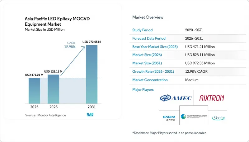
아시아태평양의 LED 에피택시 MOCVD 장비 시장 규모는 2025년에 4억 7,121만 달러로 평가되었습니다. 2026년 5억 2,811만 달러에서 2031년까지 9억 7,205만 달러에 이를 것으로 예측되며, 2026년부터 2031년에 걸쳐 CAGR 12.98%를 나타낼 전망입니다.
국내 반도체 제조 장비에 대한 정부의 강력한 지원책, 미니 LED 및 마이크로 LED 디스플레이로의 전환, 그리고 대형 GaN 웨이퍼로의 전환과 함께 중국, 대만, 일본, 한국에서의 설비 투자가 가속화되고 있습니다. 현지 업체들은 신규 반도체 제조 장비의 절반 이상을 국내 공급업체로부터 조달하라는 중국 당국의 지시를 활용하고 있으며, 디스플레이 제조업체들은 엄격한 파장 비닝 목표를 달성하기 위해 첨단 샤워헤드형 리액터 인증을 추진하고 있습니다. 갈륨 수출 규제는 지역의 자급자족을 강화하고 장기적인 공급망 재편을 촉진하는 동시에 국내 전구체 정제에 대한 잠재적 수요를 확대되고 있습니다. 동시에 AI를 활용한 인시츄 측정 기술이 신규 장비의 표준 장비로 자리 잡으면서 결함 밀도 감소와 근본 원인 분석 주기를 단축하고 있습니다. 또한, 리퍼비시 프로그램을 통해 Tier-2 팹(Tier-2 팹)이 성숙한 리액터를 활용할 수 있게 되어, 대규모 설비투자 없이도 단계적으로 생산능력을 증강할 수 있게 되었습니다.
아시아태평양의 LED 에피택시 MOCVD 장비 시장 동향과 인사이트
중국의 화합물 반도체 팹에 대한 정부 보조금 지급
중국의 '빅펀드 3기'는 국내 장비 도입을 가속화하기 위해 475억 달러가 책정되었으며, 신규 장비 구매의 절반을 현지 업체로부터 조달하도록 의무화하는 할당 규정이 마련되었습니다. 국내 시장 침투율은 2024년 25%에서 2025년 35%까지 상승하여 NAURA Technology Group과 Advanced Micro-Fabrication Equipment Inc.의 출하량을 직접적으로 증가시켰습니다. 지방정부 차원의 세제 혜택과 보조금 지원으로 팹에 대한 실질적 설비투자가 최대 30% 절감되어 멀티 웨이퍼 리액터의 추가 수주로 이어지고 있습니다. 갈륨 자원의 우위는 국가적 인센티브와 공급망 현지화를 더욱 일치시키는 요인이 되고 있습니다. 인근 말레이시아와 베트남의 LED 제조업체들은 이미 감세 무역회랑을 적용받기 위해 중국에서 제조장비를 조달하고 있어, 이 요인으로 인한 지역 파급효과가 더욱 강화되고 있습니다.
Mini 및 Micro-LED 디스플레이 수요 급증
Omdia는 전 세계 마이크로 LED 디스플레이 매출이 2025년부터 2026년까지 두 배로 증가하여 2032년까지 68억 달러에 달할 것으로 예상하고 있습니다. 2024년 미니 LED TV 출하량은 전년 대비 100% 증가한 820만 대에 달하고, 좁은 비닝 에피택셜 웨이퍼에 대한 수요를 촉진했습니다. 현재 디스플레이 공급업체들은 파장 공차 ±2.5nm를 요구하고 있으며, 이로 인해 행성형 리액터에서 샤워헤드형 리액터로의 전환이 진행되고 있습니다. Veeco의 Lumina 시리즈는 2026년 AI 서버의 광링크에 대응하는 인듐 인화물 레이저를 지속적으로 수주하여 시장 횡단적 시너지 효과를 부각시켰습니다. 칩온보드(COB) 백라이트는 공급 과잉의 위험에 직면해 있지만, 자동차 대시보드와 증강현실(AR) 헤드셋에 채택되면서 유휴 에피택셜 생산 능력을 흡수하고 있습니다.
멀티 웨이퍼 MOCVD 장비의 높은 설비 투자 비용
최첨단 200mm 배치 반응기는 300만-500만 달러의 가격대를 형성하고 있으며, 연간 매출액이 5,000만 달러 미만인 팹에게는 장벽이 되고 있습니다. 얼라이언스 MOCVD와 헬라우스 코반틱스는 리퍼브 100mm 장비에 대해 30-40% 할인을 제공하지만, 중고 시장에서 새로운 150mm 또는 200mm 장비의 가용성은 제한적입니다. 4-6년이라는 긴 투자 회수 기간은 수요 전망이 불투명한 상황에서 신규 투자에 걸림돌이 될 수 있습니다. 대만과 일본에서는 임대차 계약이 확산되고 있지만, 중국 본토의 금융기관은 여전히 신중한 태도를 유지하고 있으며, 자금 조달 경로가 제한적입니다. 따라서 설비 투자에 대한 부담이 기술 전환을 지연시켜 아시아태평양의 LED 에피택시 MOCVD 장비 시장의 단기적인 출하량 급증을 억제하고 있습니다.
부문 분석
GaN 플랫폼은 일반 조명, 백라이트, 자동차 헤드램프에 널리 사용되면서 2025년 시장 점유율 68.86%를 차지했습니다. 성숙한 전구체 생태계와 다양한 기판 선택이 GaN 다이의 비용 경쟁력을 유지하고 있으며, 아시아태평양의 LED 에피택시 MOCVD 장비 시장 도입 기반에서 우위를 점하고 있습니다. 대만 반도체 제조 회사(TSMC)의 20억 달러 규모의 갈륨 재활용 프로그램은 GaN 공급을 수출 변동에 따른 영향으로부터 더욱 보호하고 있습니다. AlGaN UV-C 디바이스는 수처리 시설 및 의료시설의 엄격한 위생 기준에 힘입어 13.24%의 예측 CAGR을 유지하고 있습니다. 유럽과 북미의 엄격한 배기가스 규제는 이미 지자체 개보수 프로젝트를 촉진하고 있으며, 1,100°C 이상의 성장 기간을 유지할 수 있는 고온 원자로에 대한 견조한 장비 주문으로 이어지고 있습니다.
공급망의 전문화가 진행되고 있습니다. 중국 및 대만의 파운드리 업체들은 AI를 활용한 인사이트 측정 기술을 활용하여 높은 스레딩 전위 밀도를 해결하고, AlGaN 에피택시 파일럿 라인의 생산 확대를 추진하고 있습니다. 한편, 유럽과 미국 업체들은 비소화인계 반응기 로드맵을 파워일렉트로닉스 및 태양열 집광기 시장으로 전환하고 있으며, 이로 인해 아시아태평양의 국내 업체들이 GaN LED의 점유율을 공고히 할 수 있게 되었습니다. 따라서 아태지역 LED 에피택시 MOCVD 장비 업계에서는 GaN이 지속적으로 수익의 주축을 이루는 가운데, AlGaN이 시너지 효과로 인한 수익률 향상으로 성장의 원동력이 될 것으로 예측됩니다.
2025년에는 150mm 부문이 시장 점유율의 46.39%를 차지했으며, 이는 대량 생산 LED 제조에서 수년간의 역할을 반영합니다. 그러나 200mm 이상 카테고리는 CAGR 13.63%를 나타낼 것으로 예측되는데, 이는 대형 기판이 다이당 비용을 낮추고 주류 실리콘 팹의 물류 체계와 일치하기 때문입니다. 가동률 향상은 엣지 제외 구역의 축소로 인한 것입니다. 이 영역은 100mm 웨이퍼의 경우 20%에 육박했지만, 200mm 로트에서는 약 8-10%까지 감소하여 평방센티미터당 유효 자본 효율이 향상되었습니다. 300mm로 원활하게 전환할 수 있는 Veeco의 Propel 플랫폼은 고객의 로드맵을 미래에 대비할 수 있도록 장비 제조업체가 추진하는 노력을 상징합니다.
그러나 이 전환은 불균일합니다. 일본과 대만의 IDM은 기존 DRAM 클린룸을 GaN 에피택시용으로 전환하여 추가적인 인프라 투자를 최소화하고 있지만, 중국 본토의 많은 팹에서는 200mm 대응을 위해 벌크 가스 시스템 및 배기가스 처리 시스템을 완전히 새로 도입하기 위한 자금 조달이 필요합니다. 자금 조달이 필요하게 되었습니다. 사파이어의 비용과 결함률로 인해 현재 일부 UV-C 및 레이저 응용 분야는 150mm로 제한되어 다경종 생태계를 유지하고 있습니다. 전반적으로, 이러한 전환 추세는 웨이퍼 크기의 변화가 아시아태평양의 LED 에피택시 MOCVD 장비 시장에서 장비 투자 타이밍에 영향을 미칠 수 있다는 점을 강조하고 있습니다.
기타 혜택 :
- 엑셀 형식 시장 예측(ME) 시트
- 3개월간 애널리스트 지원
자주 묻는 질문
목차
제1장 서론
제2장 조사 방법
제3장 주요 요약
제4장 시장 구도
제5장 시장 규모와 성장 예측
제6장 경쟁 구도
제7장 시장 기회와 향후 전망
KTH 26.05.29The Asia-Pacific LED epitaxy MOCVD equipment market size is projected to be USD 471.21 million in 2025, USD 528.11 million in 2026, and reach USD 972.05 million by 2031, growing at a CAGR of 12.98% from 2026 to 2031.
Robust state incentives for domestic semiconductor tools, the pivot toward mini-LED and micro-LED displays, and the shift to larger GaN wafers are together accelerating capital spending across China, Taiwan, Japan, and South Korea. Local equipment vendors are capitalizing on Beijing's mandate that at least half of new semiconductor tools come from domestic suppliers, while display makers are qualifying advanced showerhead reactors to meet tight wavelength-binning targets. Gallium export controls are reinforcing regional self-reliance, driving long-term supply-chain realignment, and expanding addressable demand for indigenous precursor purification. At the same time, AI-driven in-situ metrology is becoming standard on new tools, cutting defect density and shortening root-cause analysis cycles. Refurbishment programs are widening access to mature reactors for Tier-2 fabs, enabling incremental capacity additions without full capital outlays.
Asia-Pacific LED Epitaxy MOCVD Equipment Market Trends and Insights
Government Subsidies for Compound-Semiconductor Fabs in China
China's Big Fund Phase 3 set aside USD 47.5 billion to accelerate domestic tool adoption, with quotas stipulating that half of new equipment purchases come from local vendors. Domestic penetration rose from 25% in 2024 to 35% in 2025, directly lifting shipments for NAURA Technology Group and Advanced Micro-Fabrication Equipment Inc. Provincial tax holidays and subsidized industrial parks have cut effective fab capex by up to 30%, unlocking incremental orders for multi-wafer reactors. Gallium resource dominance further aligns state incentives with supply-chain localization. Neighboring Malaysian and Vietnamese LED makers are already sourcing Chinese tools to qualify for reduced-tariff trade corridors, reinforcing the driver's regional spill-over effect.
Surge in Demand for Mini and Micro-LED Displays
Omdia projects global micro-LED display revenue to double between 2025 and 2026, then scale to USD 6.8 billion by 2032. Mini-LED TV shipments climbed 100% year-over-year to 8.2 million units in 2024, lifting demand for narrow-binning epitaxial wafers. Display suppliers now require +-2.5 nm wavelength tolerance, prompting migration from planetary to showerhead reactors. Veeco's Lumina series logged repeat orders in 2026 for indium-phosphide lasers that support AI-server optical links, highlighting cross-market synergies. Although chip-on-board backlighting faces oversupply risk, adoption in automotive dashboards and augmented-reality headsets is absorbing idle epi capacity.
High Capital Cost of Multi-Wafer MOCVD Tools
State-of-the-art 200 mm batch reactors carry USD 3-5 million price tags, a hurdle for fabs with annual sales below USD 50 million. Although Alliance MOCVD and Heraeus Covantics offer 30-40% discounts on refurbished 100 mm equipment, availability of newer 150 mm or 200 mm tools in the secondary market is limited. Long four-to-six-year payback periods discourage greenfield investment when demand visibility narrows. Leasing structures are emerging in Taiwan and Japan, yet mainland China lenders remain cautious, keeping financing channels constrained. The capex burden therefore delays technology transitions and tempers short-term shipment spikes for the Asia-Pacific LED epitaxy MOCVD equipment market.
Other drivers and restraints analyzed in the detailed report include:
- Shift to 150 mm and 200 mm GaN Wafers for Cost Reduction
- Increasing Adoption of UV-C LED Disinfection Systems
- Oversupply Risk in LED Backlighting Market
For complete list of drivers and restraints, kindly check the Table Of Contents.
Segment Analysis
GaN platforms anchored 68.86% of the market share in 2025, thanks to entrenched use in general lighting, backlighting, and automotive headlamps. Mature precursor ecosystems and substrate optionality keep GaN die costs competitive, reinforcing the Asia-Pacific LED epitaxy MOCVD equipment market's installed base advantage. Taiwan Semiconductor Manufacturing Company's USD 2 billion gallium recycling program is further insulating GaN supply from export volatility. AlGaN UV-C devices sit at a smaller baseline yet carry a 13.24% forecast CAGR, buoyed by stringent hygiene mandates in water-treatment and healthcare facilities. Tight emission regulations in Europe and North America are already spurring municipal retrofit projects, translating into firm tool orders for high-temperature reactors that can sustain >1,100 °C growth windows.
Supply-chain specialization is deepening. Chinese and Taiwanese foundries are ramping AlGaN epi pilot lines, leveraging AI-driven in-situ metrology to tackle high threading-dislocation density. Western vendors, meanwhile, are redirecting arsenide-phosphide reactor roadmaps toward power electronics and solar concentrator markets, allowing domestic APAC players to consolidate GaN LED share. The Asia-Pacific LED epitaxy MOCVD equipment industry therefore expects GaN to remain the revenue anchor, while AlGaN provides the incremental growth zest that lifts blended margins.
In 2025, the 150 mm segment accounted for 46.39% of the market share, reflecting its long-standing role in volume LED manufacturing. Yet the 200 mm and above category is charted to post a 13.63% CAGR, as larger substrates lower per-die cost and align with mainstream silicon fab logistics. Utilization improvements stem from smaller edge exclusion zones, which drop from near 20% on 100 mm wafers to roughly 8-10% on 200 mm lots, enhancing effective capital-per-square-centimeter economics. Veeco's Propel platform, capable of seamless 300 mm transitions, illustrates equipment makers' push to future-proof customer roadmaps.
The transition, however, is uneven. Japanese and Taiwanese IDMs have re-purposed legacy DRAM cleanrooms for GaN epi, minimizing incremental infrastructure spend, whereas many mainland Chinese fabs must finance entirely new bulk-gas and abatement systems for 200 mm readiness. Sapphire cost and defectivity currently limit some UV-C and laser applications to 150 mm, preserving a multi-diameter ecosystem. Overall, migration dynamics underscore how wafer-size shifts can swing capex timing for the Asia-Pacific LED epitaxy MOCVD equipment market.
The Asia-Pacific LED Epitaxy MOCVD Equipment Market Report is Segmented by LED Material System (GaN-Based LED Epitaxy Systems, and More), Wafer Size Capability (Up To 100mm, 150mm, and 200mm and Above), Reactor Configuration (Planetary Reactors, and Showerhead Reactors), End User (Integrated LED Manufacturers, and Epitaxy Foundries and Merchant Epi Suppliers), and Country. The Market Forecasts are Provided in Terms of Value (USD).
List of Companies Covered in this Report:
- AIXTRON SE
- Veeco Instruments Inc.
- Advanced Micro-Fabrication Equipment Inc. (AMEC)
- NAURA Technology Group Co. Ltd.
- Taiyo Nippon Sanso Corporation
- ASM International N.V.
- Tokyo Electron Ltd.
- Applied Materials Inc.
- topecsh Co. Ltd.
- CVD Equipment Corporation
- NuFlare Technology Inc.
- Jusung Engineering Co. Ltd.
- Element 3-5 GmbH
- Alliance MOCVD LLC
- Suzhou Powerway Wafer Co. Ltd.
- Sanan Optoelectronics Co. Ltd.
- Epistar Corporation
- Silan Azure Co. Ltd.
Additional Benefits:
- The market estimate (ME) sheet in Excel format
- 3 months of analyst support
TABLE OF CONTENTS
1 INTRODUCTION
- 1.1 Study Assumptions and Market Definition
- 1.2 Scope of the Study
2 RESEARCH METHODOLOGY
3 EXECUTIVE SUMMARY
4 MARKET LANDSCAPE
- 4.1 Market Overview
- 4.2 Market Drivers
- 4.2.1 Government Subsidies for Compound-Semiconductor Fabs in China
- 4.2.2 Surge in Demand for Mini and Micro-LED Displays
- 4.2.3 Shift to 150 mm and 200 mm GaN Wafers for Cost Reduction
- 4.2.4 Increasing Adoption of UV-C LED Disinfection Systems
- 4.2.5 AI-Driven In-Situ Metrology Integration Reducing Yield Loss
- 4.2.6 Circular Reactor Refurbishment Programs Lowering CapEx
- 4.3 Market Restraints
- 4.3.1 High Capital Cost of Multi-Wafer MOCVD Tools
- 4.3.2 Oversupply Risk in LED Backlighting Market
- 4.3.3 Volatile Trimethylgallium and Ammonia Supply Chains
- 4.3.4 Shortage of Experienced Epitaxy Engineers in Tier-2 Cities
- 4.4 Industry Supply Chain Analysis
- 4.5 Technological Outlook
- 4.6 Regulatory Landscape
- 4.7 Impact of Macroeconomic Factors on the Market
- 4.8 Porter's Five Forces Analysis
- 4.8.1 Threat of New Entrants
- 4.8.2 Bargaining Power of Suppliers
- 4.8.3 Bargaining Power of Buyers
- 4.8.4 Threat of Substitutes
- 4.8.5 Intensity of Competitive Rivalry
5 MARKET SIZE AND GROWTH FORECASTS (VALUE)
- 5.1 By LED Material System
- 5.1.1 GaN-based LED Epitaxy Systems
- 5.1.2 AlGaN UV LED Epitaxy Systems
- 5.1.3 AlInGaP LED Epitaxy Systems
- 5.2 By Wafer Size Capability
- 5.2.1 Upto 100 mm
- 5.2.2 150 mm
- 5.2.3 200 mm and Above
- 5.3 By Reactor Configuration
- 5.3.1 Planetary Reactors
- 5.3.2 Showerhead Reactors
- 5.4 By End User
- 5.4.1 Integrated LED Manufacturers (IDMs)
- 5.4.2 Epitaxy Foundries and Merchant Epi Suppliers
- 5.5 By Country
- 5.5.1 China
- 5.5.2 Japan
- 5.5.3 Taiwan
- 5.5.4 Rest of Asia-Pacific
6 COMPETITIVE LANDSCAPE
- 6.1 Market Concentration
- 6.2 Strategic Moves
- 6.3 Market Share Analysis
- 6.4 Company Profiles (Includes Global Level Overview, Market Level Overview, Core Segments, Financials as Available, Strategic Information, Market Rank/Share, Products and Services, and Recent Developments)
- 6.4.1 AIXTRON SE
- 6.4.2 Veeco Instruments Inc.
- 6.4.3 Advanced Micro-Fabrication Equipment Inc. (AMEC)
- 6.4.4 NAURA Technology Group Co. Ltd.
- 6.4.5 Taiyo Nippon Sanso Corporation
- 6.4.6 ASM International N.V.
- 6.4.7 Tokyo Electron Ltd.
- 6.4.8 Applied Materials Inc.
- 6.4.9 topecsh Co. Ltd.
- 6.4.10 CVD Equipment Corporation
- 6.4.11 NuFlare Technology Inc.
- 6.4.12 Jusung Engineering Co. Ltd.
- 6.4.13 Element 3-5 GmbH
- 6.4.14 Alliance MOCVD LLC
- 6.4.15 Suzhou Powerway Wafer Co. Ltd.
- 6.4.16 Sanan Optoelectronics Co. Ltd.
- 6.4.17 Epistar Corporation
- 6.4.18 Silan Azure Co. Ltd.
7 MARKET OPPORTUNITIES AND FUTURE OUTLOOK
- 7.1 White-Space and Unmet-Need Assessment


