
|
시장보고서
상품코드
2062073
반도체 본딩 시장 : 점유율 분석, 업계 동향과 통계, 성장 예측(2026-2031년)Semiconductor Bonding - Market Share Analysis, Industry Trends & Statistics, Growth Forecasts (2026 - 2031) |
||||||
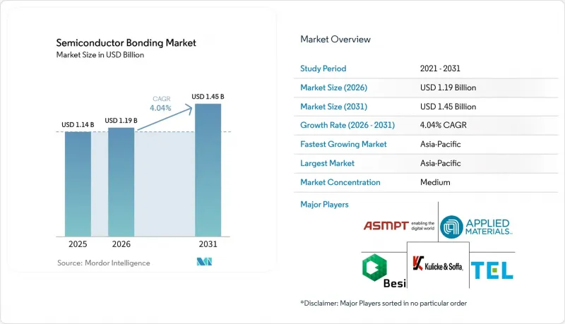
Mordor Intelligence에 의하면, 반도체 본딩 시장 규모는 2025년 11억 4,000만 달러에서 2026년에는 11억 9,000만 달러로 확대되어 2026년부터 2031년까지 CAGR 4.04%로 성장을 지속하여, 2031년까지 14억 5,000만 달러에 이를 것으로 예측됩니다.

본 보고서는 장비 유형(다이 본더, 웨이퍼 본더 등), 상호 연결 수준(다이 간 등), 용도(MEMS 및 센서 등), 최종 이용 산업(소비자 가전, 자동차·모빌리티 등), 그리고 지역(아시아태평양, 북미, 유럽, 남미, 중동 및 아프리카)별로 분류되어 있습니다. 시장 전망은 금액(달러) 기준으로 제시되어 있습니다.
세계 반도체 본딩 시장 동향과 인사이트
고급 패키징 및 소형화에 대한 수요 증가
이기종 치플렛을 통해 파운드리 업체는 로직, 메모리, 아날로그 다이를 10마이크로미터 미만의 피치로 적층할 수 있게 되어, 마이크로 범프를 제거하고 기생 용량을 80% 줄일 수 있습니다. UCIe 3.0은 64GT/s의 링크 속도를 구현하며, AI 가속기에 제곱mm당 최대 4 TB/s의 대역폭을 제공합니다. 인텔 포베로스 직접(Intel Foveros Direct)는 플립 칩 패키징보다 15배 높은 상호 연결 밀도를 구현하며, 데이터센터용 타일에서 300W의 열 설계 전력(TDE)을 지원합니다. 유리 기판은 시제품 단계에 접어들었으며, 유기 소재에 비해 뒤틀림이 10분의 1로 줄어들어 패널 수준의 비용을 30% 절감합니다. 그 결과, 반도체 본딩 시장에서는 플라즈마 활성화, 정렬, 열압축을 하나의 툴 클러스터로 통합한 하이브리드 본더에 대해 사상 최대의 수주가 들어오고 있습니다.
소비자용 전자기기 및 자동차 분야의 확대
웨이퍼 레벨 칩 스케일 패키징(Wafer Level Chip Scale Packaging)을 통해 CMOS(상보형 금속 산화막 반도체) 이미지 센서의 두께가 40% 줄어들어, 더 얇은 스마트폰과 멀티 카메라를 탑재한 차량의 구현이 가능해집니다. 자동차용 CIS의 출하 대수는 2029년까지 12억 대에 달하고, 매출액은 84억 달러에 이를 것으로 전망됩니다. 실리콘 카바이드(SiC) 트랙션 인버터에는 200°C를 견딜 수 있는 다이 어태치 기술이 필요하며, 이로 인해 새로운 EV 플랫폼에서 소결 은의 채택 비율은 50%를 넘어섰습니다. 구리선은 이미 자동차용 본딩 시장의 38%를 차지하고 있으며, AEC-Q006 공정의 성숙에 따라 2027년까지 45%를 넘어설 것으로 전망됩니다. 이러한 추세에 따라 고출력 모듈과 광 모듈이 첨단 패키징 공정에 도입되면서 시장이 확대되고 있습니다.
높은 설비 투자 및 운영 비용
하이브리드 본딩 장비는 1대당 500만-8,000만 달러, 전체 라인의 경우 3,000만 달러를 초과하기 때문에 평균 10%인 OSAT(반도체 조립·시험 수탁)의 이익률을 압박하고 있습니다. 설계 규정이 고객의 인증 요건에 맞추어 발전함에 따라, 초기 가동률은 50% 전후에 그치며, 투자 회수 기간은 3년 이상 소요될 것으로 보입니다. 미국과 유럽의 인건비는 아시아에 비해 40-50% 높으며, CMP(화학적 기계 연마) 소모품은 웨이퍼 1장당 15-20달러로, 플립칩 언더필 비용의 3배에 달하고, 영업 비용을 압박하고 있습니다. 이러한 요인들이 반도체 본딩 시장의 단기적인 성장을 저해하고 있습니다.
부문별 분석
다이본더 장비는 고정밀 공융 및 에폭시 부착 기술이 파워 및 RF 부품의 핵심 기술로 자리매김함에 따라 2025년 매출의 36.77%를 차지했습니다. 플립 칩 본더는 40-150μm 피치를 지원하며 시간당 5,000개 이상의 생산 능력을 갖추고 있는 반면, 와이어 본더는 비용 효율성을 중시하는 조립 분야에서 주류를 이루고 있습니다. 웨이퍼 본더는 MEMS 및 3D NAND의 구현을 가능하게 하며, 다이 레벨 캡핑에 비해 30-40%의 비용 절감을 실현함으로써 레거시 디바이스용 반도체 본딩 시장 규모를 지탱하고 있습니다.
하이브리드 본더는 HBM4, 칩렛 및 코패키지드 옵틱스에서 10μm 미만의 피치가 요구되기 때문에 2031년까지 연평균 성장률(CAGR) 4.27%라는 가장 높은 성장세를 보일 것으로 전망됩니다. EV Group의 GEMINI 플랫폼은 플럭스 프리 본딩에 350 kN의 힘을 가하며, Applied-Besi Kinex 클러스터는 사이클 타임을 40% 단축합니다. TSMC의 CoWoS 양산에는 약 15억 달러 상당의 장비 약 250대가 투입되어, 설비 투자 의지가 높다는 점이 입증되었습니다. 다이아타치 라인의 높은 가동률이 지속되는 가운데, 시장은 지출을 하이브리드 클러스터 툴로 재분배하고 있습니다.
UCIe 규격에 따라 대역폭이 mm²당 4TB/s까지 향상되고, AI 가속기가 로직과 HBM4 타일을 결합할 수 있게 됨에 따라, 2025년 매출의 53.91%를 다이 간 본딩이 차지했습니다. 인텔(Intel)의 EMIB는 풀 인터포저를 사용하지 않고 55μm 피치로 다이를 연결하며, 암코어(Amkor)는 현재 애리조나주와 한국에서 EMIB 서비스를 제공합니다. 이 토폴로지는 2026년부터 2029년까지의 로드맵의 기반이 되며, 반도체 본딩 시장에서 가장 큰 점유율을 차지하고 있습니다.
3D NAND가 400층을 돌파하고 1,000층 스택을 목표로 하고 있는 만큼, 웨이퍼 간 하이브리드 본딩 시장은 예측 기간(2026-2031년) 동안 연평균 성장률(CAGR) 4.52%로 성장할 것으로 전망됩니다. 삼성, YMTC, 키오크시아는 모두 웨이퍼 단계에서 메모리 아래에 CMOS 로직을 본딩하고 있으며, 이를 통해 수율을 25% 향상시켰습니다. 다이-투-웨이퍼 본딩은 정상 작동이 확인된 다이를 수동형 웨이퍼 위에 실장하는 CIS 및 RF 소자를 지원합니다. 이러한 통합된 흐름은 메모리, 로직, 센서 노드에 걸친 반도체 본딩 시장의 확대를 가속화하고 있습니다.
지역별 분석
아시아태평양은 2025년 매출의 41.53%를 차지해, 2031년까지 연평균 성장률(CAGR) 4.91%로 성장할 것으로 전망되는데, 이는 지역별로는 가장 높은 성장률입니다. TSMC는 2026년까지 CoWoS 생산 능력을월12,000 웨이퍼에서 50,000 웨이퍼로 확대하고, AI 가속기용 생산을 위해 자이(Chiayi)에 팹 건설을 착공했습니다. 한국은 2,300억 달러 규모의 계획을 통해 Samsung Electronics 용인 공장과 SK하이닉스의 P&T7에 자금을 투입해, 2028년까지 국내 HBM 생산량을 3배로 확대할 예정입니다. 중국의 232층 NAND ‘XTacking’ 기술은 수출 규제 대상 도구를 우회하고 있는 반면, 일본은 도쿄 일렉트로ンの 연구개발에 1조 5,000억 엔(93억 달러)을 투자하고 있습니다. 지역별 공급 집중은 숙련된 인력, 공급업체 및 보조금을 한곳에 모음으로써 반도체 본딩 시장을 활성화하고 있습니다.
북미는 364억 달러 규모의 CHIPS 법 지원금의 혜택을 받고 있으며, 암콜의 애리조나 공장과 SK하이닉스의 인디애나주 HBM 생산 라인이 첨단 패키징 역량의 핵심을 담당하고 있습니다. 인텔은 EMIB 패키징을 암콜에 외주했으며, 마이크론은 DRAM 생산량을 확대하기 위해 PSMC의 P5 팹에 18억 달러를 투자했습니다. 멕시코는 인건비가 60% 저렴하다는 장점을 살려 와이어 본딩 업무의 니어쇼어링을 유치하고 있으며, 텍사스주 파브로의 물류 시간을 40% 단축하고 있습니다. 이 정책은 리소그래피가 아닌 패키징에 중점을 두고 있으며, 북미 시장의 견실한 성장을 위한 기반을 마련하고 있습니다.
유럽은 IPCEI-ME를 통해 430억 유로(486억 2,000만 달러)를 확보했으며, 이 중 25억 유로(28억 3,000만 달러)가 NanoIC의 하이브리드 본딩 키트에 배정되었습니다. TSMC는 2027년부터 가동을 예정하고 있는 드레스덴의 300mm 팹에 100억 유로(113억 1,000만 달러)를 투자하며, 인텔의 마그데부르크 사업장에서는 2029년까지 초기 생산을 시작하는 것을 목표로 하고 있습니다. 허가 및 인가 절차로 인해 아시아에 비해 18-24개월 정도 지연되는 반면, 자본 유입으로 인해 현지 본딩 수요는 확대되고 있습니다. 남미는 여전히 기존 기술에 중점을 두고 있으며, 중동의 프로젝트는 아직 탐색 단계에 있습니다. 이러한 영향들을 종합해 보면, 반도체 본딩 시장은 아시아에 집중된 상태를 유지하고 있지만, 지정학적 발자취는 다양화되고 있습니다.
기타 혜택:
- 엑셀 형식 시장 예측(ME) 시트
- 3개월간의 애널리스트 지원
자주 묻는 질문
목차
제1장 서론
제2장 조사 방법
제3장 주요 요약
제4장 시장 구도
제5장 시장 규모와 성장 예측
제6장 경쟁 구도
제7장 시장 기회와 향후 전망
JHS 26.06.19According to Mordor Intelligence, the semiconductor bonding market size is expected to grow from USD 1.14 billion in 2025 to USD 1.19 billion in 2026 and is forecast to reach USD 1.45 billion by 2031 at 4.04% CAGR over 2026-2031.
This report is Segmented by Equipment Type (Die Bonder, Wafer Bonder, and More), Interconnect Level (Die-To-Die, and More), Application (MEMS and Sensors, and More), End-Use Industry (Consumer Electronics, Automotive and Mobility, and More), and Geography (Asia-Pacific, North America, Europe, South America, and Middle East and Africa). The Market Forecasts are Provided in Terms of Value (USD).
Global Semiconductor Bonding Market Trends and Insights
Growing Demand for Advanced Packaging and Miniaturization
Heterogeneous chiplets allow foundries to stack logic, memory, and analog dies at sub-10 micrometer pitches, removing micro-bumps and lowering parasitic capacitance by 80%. UCIe 3.0 enables 64 GT/s links, giving AI accelerators up to 4 TB/s bandwidth per square millimeter. Intel Foveros Direct reaches 15 times the interconnect density of flip-chip packaging, supporting 300 W thermal-design envelopes for datacenter tiles. Glass substrates enter pilot production with 10-times lower warpage than organic materials and cut panel-level cost by 30%. As a result, the semiconductor bonding market attracts record orders for hybrid bonders that integrate plasma activation, alignment, and thermocompression in one tool cluster.
Expansion of Consumer Electronics and Automotive Sectors
Wafer-level chip-scale packaging shrinks CMOS (Complementary Metal-Oxide-Semiconductor) image-sensor height by 40%, enabling thinner phones and multi-camera vehicles. Automotive CIS shipments are projected to hit 1.2 billion units by 2029, equivalent to USD 8.4 billion in revenue. Silicon carbide traction inverters need die-attach that survives 200°C, pushing adoption of sintered silver past 50% share in new EV platforms. Copper wire already represents 38% of automotive bonds and will pass 45% by 2027 as AEC-Q006 processes mature. These trends expand the market by drawing high-power and optical modules into advanced-packaging flows.
High Capital Investment and Operational Costs
Hybrid-bonding tools cost USD 5-8 million each, and a full line tops USD 30 million, straining OSAT (Outsourced Semiconductor Assembly and Test) margins that average 10%. Early utilization stays near 50% because design rules evolve alongside customer qualifications, stretching payback beyond three years. Labor in the United States and Europe is 40-50% pricier than in Asia, and CMP consumables run USD 15-20 per wafer, triple flip-chip underfill expense, pressuring opex. These factors temper near-term expansion of the semiconductor bonding market.
Other drivers and restraints analyzed in the detailed report include:
- Rising Adoption of 3D Integration and MEMS Devices
- AI-Driven Heterogeneous Integration for Edge Computing
- Process Complexity at Advanced Nodes
For complete list of drivers and restraints, kindly check the Table Of Contents.
Segment Analysis
Die Bonder Equipment retained 36.77% of 2025 revenue as high-precision eutectic and epoxy attach remain core for power and RF components. Flip-chip bonders address 40-150 µm pitches at volumes over 5,000 units per hour, while wire bonders dominate cost-sensitive assemblies. Wafer bonders enable MEMS and 3D NAND with 30-40% cost savings over die-level capping, anchoring the semiconductor bonding market size for legacy devices.
Hybrid bonders will post the quickest 4.27% CAGR through 2031 because HBM4, chiplets, and co-packaged optics require less than 10 µm pitches. EV Group's GEMINI platform applies 350 kN forces for flux-free bonding, and the Applied-Besi Kinex cluster cuts cycle time by 40%. TSMC's CoWoS ramp consumed about 250 tools valued at nearly USD 1.5 billion, confirming capital appetite. The market reallocates spend toward hybrid cluster tools even while die-attach lines run at high utilization.
Die-to-die bonding controlled 53.91% of 2025 revenue because UCIe standards lift bandwidth to 4 TB/s mm2, letting AI accelerators pair logic with HBM4 tiles. Intel EMIB connects dies at 55 µm pitch without full interposers, and Amkor now offers EMIB in Arizona and Korea. This topology anchors 2026-2029 roadmaps and secures the largest semiconductor bonding market share.
Wafer-to-wafer hybrid bonding is projcted to grow at 4.52% CAGR during the forecast period (2026-2031) as 3D NAND sails past 400 layers and targets 1,000-layer stacks. Samsung, YMTC, and Kioxia all bond CMOS logic under memory at the wafer level, improving yield by 25%. Die-to-wafer bonding supports CIS and RF devices where known-good dies mount onto passive wafers. These combined flows reinforce the semiconductor bonding market breadth across memory, logic, and sensor nodes.
Geography Analysis
Asia-Pacific generated 41.53% of 2025 revenue and is forecast to grow 4.91% CAGR through 2031, the highest regional pace. TSMC raised CoWoS capacity from 12,000 to 50,000 wafers per month by 2026 and broke ground on a Chiayi fab aimed at AI accelerators. South Korea's USD 230 billion plan funds Samsung Yongin and SK Hynix P&T7, tripling domestic HBM output by 2028. China's XTacking 232-layer NAND avoids restricted tools, while Japan funnels JPY 1.5 trillion (USD 9.3 billion) into Tokyo Electron research and development. Regional supply concentration feeds the semiconductor bonding market by pooling skilled labor, suppliers, and subsidies.
North America benefits from USD 36.4 billion CHIPS Act grants, with Amkor's Arizona plant and SK Hynix's Indiana HBM line anchoring advanced-packaging capacity. Intel outsources EMIB packaging to Amkor, and Micron paid USD 1.8 billion for PSMC's P5 fab to expand DRAM volume. Mexico draws nearshoring wire-bonding jobs at 60% lower labor cost, trimming logistics times to Texas fabs by 40%. The policy focuses on packaging, versus lithography, and positions the market for resilient North American growth.
Europe secured EUR 43 billion (USD 48.62 billion) under IPCEI-ME, with EUR 2.5 billion (USD 2.83 billion) for NanoIC hybrid-bonding kits. TSMC commits EUR 10 billion (USD 11.31 billion) for a 300 mm fab in Dresden, starting 2027, and Intel's Magdeburg site targets initial output by 2029. Although timelines extend 18-24 months longer than in Asia due to permitting, the capital inflow enlarges local bonding demand. South America remains legacy-focused, and Middle East projects are exploratory. Net impact keeps the semiconductor bonding market concentrated in Asia yet diversifies geopolitical footprints.
- ADVANTEST CORPORATION
- Amkor Technology
- Applied Materials, Inc.
- ASMPT
- Besi
- EV Group (EVG)
- HANMI INCHEON
- Hesse GmbH
- Kulicke and Soffa Industries, Inc
- Mycronic
- Nitto Denko Corporation
- Nordson Corporation
- Onto Innovation
- Palomar Technologies
- SHINKO ELECTRIC INDUSTRIES
- SUSS MicroTec SE
- Tokyo Electron Limited
- TORAY ENGINEERING Co., Ltd.
- TPT Wire Bonder GmbH & Co KG
- Yamaha Robotics
Additional Benefits:
- The market estimate (ME) sheet in Excel format
- 3 months of analyst support
TABLE OF CONTENTS
1 Introduction
- 1.1 Study Assumptions and Market Definition
- 1.2 Scope of the Study
2 Research Methodology
3 Executive Summary
4 Market Landscape
- 4.1 Market Overview
- 4.2 Market Drivers
- 4.2.1 Growing demand for advanced packaging and miniaturization
- 4.2.2 Expansion of consumer electronics and automotive sectors
- 4.2.3 Rising adoption of 3D integration and MEMS devices
- 4.2.4 AI-driven heterogeneous integration for edge computing
- 4.2.5 Government semiconductor subsidy races reshaping regional bonding capacity
- 4.3 Market Restraints
- 4.3.1 High capital investment and operational costs
- 4.3.2 Process complexity at advanced nodes
- 4.3.3 Limited availability of ultra-flat wafers for hybrid bonding
- 4.4 Value Chain Analysis
- 4.5 Porter's Five Forces
- 4.5.1 Threat of New Entrants
- 4.5.2 Bargaining Power of Buyers
- 4.5.3 Bargaining Power of Suppliers
- 4.5.4 Threat of Substitutes
- 4.5.5 Competitive Rivalry
5 Market Size and Growth Forecasts (Value)
- 5.1 By Equipment Type
- 5.1.1 Die Bonder Equipment
- 5.1.2 Wafer Bonder Equipment
- 5.1.3 Flip-Chip Bonder Equipment
- 5.1.4 Wire Bonder Equipment
- 5.1.5 Hybrid Bonder Equipment
- 5.2 By Interconnect Level
- 5.2.1 Die-to-Die Bonding
- 5.2.2 Die-to-Wafer Bonding
- 5.2.3 Wafer-to-Wafer Bonding
- 5.3 By Application
- 5.3.1 RF Devices
- 5.3.2 MEMS and Sensors
- 5.3.3 CMOS Image Sensors
- 5.3.4 LED
- 5.3.5 3D NAND
- 5.4 By End-use Industry
- 5.4.1 Consumer Electronics
- 5.4.2 Automotive and Mobility
- 5.4.3 Industrial and Automation
- 5.4.4 Healthcare and Life-Sciences
- 5.4.5 Telecommunications and Datacom
- 5.4.6 Aerospace and Defense
- 5.4.7 Other End-user Industries (Energy and More)
- 5.5 By Geography
- 5.5.1 Asia-Pacific
- 5.5.1.1 China
- 5.5.1.2 Japan
- 5.5.1.3 India
- 5.5.1.4 South Korea
- 5.5.1.5 Taiwan
- 5.5.1.6 Rest of APAC
- 5.5.2 North America
- 5.5.2.1 United States
- 5.5.2.2 Canada
- 5.5.2.3 Mexico
- 5.5.3 South America
- 5.5.3.1 Brazil
- 5.5.3.2 Argentina
- 5.5.3.3 Rest of South America
- 5.5.4 Europe
- 5.5.4.1 Germany
- 5.5.4.2 United Kingdom
- 5.5.4.3 France
- 5.5.4.4 Italy
- 5.5.4.5 Russia
- 5.5.4.6 Rest of Europe
- 5.5.5 Middle-East and Africa
- 5.5.5.1 Saudi Arabia
- 5.5.5.2 South Africa
- 5.5.5.3 Middle-East and Africa
- 5.5.1 Asia-Pacific
6 Competitive Landscape
- 6.1 Market Concentration
- 6.2 Strategic Moves
- 6.3 Market Share(%)/Ranking Analysis
- 6.4 Company Profiles (includes Global-level Overview, Market-level Overview, Core Segments, Financials as available, Strategic Information, Products and Services, Recent Developments)
- 6.4.1 ADVANTEST CORPORATION
- 6.4.2 Amkor Technology
- 6.4.3 Applied Materials, Inc.
- 6.4.4 ASMPT
- 6.4.5 Besi
- 6.4.6 EV Group (EVG)
- 6.4.7 HANMI INCHEON
- 6.4.8 Hesse GmbH
- 6.4.9 Kulicke and Soffa Industries, Inc
- 6.4.10 Mycronic
- 6.4.11 Nitto Denko Corporation
- 6.4.12 Nordson Corporation
- 6.4.13 Onto Innovation
- 6.4.14 Palomar Technologies
- 6.4.15 SHINKO ELECTRIC INDUSTRIES
- 6.4.16 SUSS MicroTec SE
- 6.4.17 Tokyo Electron Limited
- 6.4.18 TORAY ENGINEERING Co., Ltd.
- 6.4.19 TPT Wire Bonder GmbH & Co KG
- 6.4.20 Yamaha Robotics
7 Market Opportunities and Future Outlook
- 7.1 White-space and Unmet-Need Assessment
