
|
시장보고서
상품코드
2062168
흑린 : 시장 점유율 분석, 업계 동향 및 통계, 성장 예측(2026-2031년)Black Phosphorus - Market Share Analysis, Industry Trends & Statistics, Growth Forecasts (2026 - 2031) |
||||||
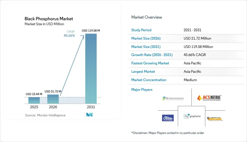
Mordor Intelligence에 의하면, 2025년에 1,544만 달러 규모인 흑린 시장은 2026년에는 2,172만 달러로 확대되어 2031년까지 1억 1,958만 달러에 이를 것으로 예측됩니다.
2026년부터 2031년까지의 연평균 성장률(CAGR)은 40.66%가 될 것으로 전망됩니다.

본 보고서는 형태(분말, 결정, 박리 나노시트, 박막), 용도(일렉트로믹스 및 반도체, 에너지 저장, 포토닉스·광전자, 생의학·바이오센서, 환경 촉매·수처리, 기타), 지역(아시아태평양, 북미, 유럽, 남미, 중동 및 아프리카)별로 분류되어 있습니다. 시장 전망은 금액(달러) 기준으로 제시되어 있습니다.
세계의 흑린 시장 동향 및 분석
플렉서블 및 고주파 전자 분야에서 2차원 반도체 수요 급증
2024년, 초음파 화학법을 통해 박리된 흑린으로 제조된 나노리본 트랜지스터는 온/오프 비율 1.7×10⁶, 이동도 1,506 cm²V-¹s-¹을 나타내며, 5 nm 미만의 로드맵 기준을 충족했습니다. 이러한 채택을 뒷받침하는 주요 요인 중 하나는 0.29 eV에서 0.64 eV 범위 내에서 변화하는 폭 의존적 밴드갭입니다. 이러한 특성 덕분에 설계자는 합금화 공정에 구애받지 않고 논리 레벨을 변경할 수 있어 설계의 유연성을 확보할 수 있습니다. 또 다른 중요한 요인은 재료의 면내 이방성으로, 이를 통해 방향성을 가진 전하 제어가 가능해집니다. 이 특성은 정확한 전하 제어가 필수적인 굽힘 가능한 디스플레이와 같은 용도에서 특히 중요합니다. 매끄러운 에지를 가진 채널을 채택함으로써 쇼트 채널 효과가 억제되어, 실리콘에서는 일반적으로 누설 전류 문제가 심해지는 20 nm 미만의 게이트 길이에서도 트랜스컨덕턴스 수준이 200µSµm-1 이상을 유지할 수 있게 됩니다. 또한, 150°C 미만의 전이 온도에서 작동할 수 있다는 점은 웨어러블 기술에 일반적으로 사용되는 폴리이미드 기판의 요구 사항을 충족하므로, 제조업체에게 중요한 요소가 됩니다. 또한, NSF의 지원을 받아 2026년에 도입된 표면 배위 화학 기술을 통해 최대 1개월간의 상온 안정성을 실현했습니다. 이러한 안정성은 해당 트랜지스터의 상용화를 가속화하는 데 중요한 역할을 할 것으로 기대됩니다. 흑린 시장 업스트림의 수익원.
BP 기반 광집적회로의 급속한 보급
Iris Light Technologies사는 NanoBLACK(TM)을 사용하여 표준 CMOS 웨이퍼에서 1,550 nm 파장에서 11.2 A W-¹라는 놀라운 감도를 달성했습니다. 트위스트 적층 소자를 채택함으로써 감지 능력을 2,700 nm까지 확장하고, 암호화된 자유 공간 광학 시스템에 필수적인 기능인 양극성 원편광 식별 기능을 탑재했습니다. 면외 변형 제어를 통해 열 부하가 없는 상태에서도 -3%의 압축 하에서 공진 모드를 100 nm 이상 적색 편이시키는 데 성공함으로써, 고밀도 포토닉 배선의 길을 열었습니다. 이 소재는 근적외선 스펙트럼에서 양자 효율 면에서 이황화 몰리브덴을 능가할 뿐만 아니라, 그래핀과 달리 밴드갭을 가지고 있어 효율적인 변조가 가능합니다. AFRL이 체결한 2025년 계약은 이러한 진전을 국방 등급 중적외선 시스템에 적용하는 데 대한 최종 사용자의 신뢰를 입증하는 것입니다.
상온 대기 조건에서의 불안정성과 높은 봉입 비용
보호 처리가 되지 않은 나노시트는 72시간 이내에 자외선 및 가시광선 흡수율이 60%나 급격히 떨어집니다. 이러한 열화로 인해 글러브 박스 내에서의 취급 및 다층 차단막의 사용이 필요하게 되며, 이로 인해 총 비용이 최대 50%까지 증가할 가능성이 있습니다. 옥살리플라틴과의 배위 결합을 통해 흡수 유지율은 62%까지 향상됩니다. 세포막 코팅을 통해 유지율은 78%까지 더욱 향상되지만, 층을 추가할 때마다 재료비와 인건비가 증가합니다. 폴리도파민 필름은 이러한 나노시트의 수명을 몇 주까지 연장할 수 있지만, 이러한 개선에는 원자재 비용이 30% 증가하는 대가가 따릅니다. PLGA에 주입하면 서방형 방출 메커니즘을 제공하지만, 35-45%의 비용 증가로 이어집니다. 피틴산을 이용한 전기화학적 박리 공정은 가장자리가 부동태화된 플레이크를 생성하여, 캡슐화 후의 후처리를 최소화할 수 있습니다. 그러나 처리 능력은 1배치당 10그램 미만에 그치고 있어, 이로 인해 산업적 실용성이 제한되고 있습니다. 배터리 제조업체들은 흑연과의 경쟁력을 유지하기 위해 음극재 가격을 1그램당 5달러 미만으로 억제해야 한다는 과제에 직면해 있습니다. 이에 반해, 포토닉스 분야의 구매자들은 더 유연하며, 1그램당 500-1,000달러를 지불할 의사가 있고, 간접비 관리도 용이합니다.
부문별 분석
2025년, 분말은 흑린 시장 점유율의 36.67%를 차지했습니다. 이는 불규칙한 형태에도 대응할 수 있는 배터리용 슬러리 및 촉매로의 응용이 뒷받침한 결과입니다. 1그램당 800-1,200달러 가격대의 박리 나노시트는 41.23%의 성장률을 기록하며 시장이 확대될 것으로 예측됩니다. 이러한 성장은 10 nm 미만의 두께와 원자 수준에서 매끄러운 가장자리를 요구하는 디바이스 엔지니어들 수요 증가에 기인합니다. 흑린 나노 시트 시장 규모는 2026년 570만 달러에서 2031년까지 3,600만 달러로 확대될 것으로 전망됩니다. 순도 99.999% 이상의 결정은 연구 목적으로 계속해서 주목을 받고 있습니다. 그러나 웨이퍼 규모의 화학기상증착법과의 경쟁으로 인해 그 시장 점유율은 하락할 가능성이 있습니다. 분자선 에피택시 등의 박막 형성 방법에서는 현재 디바이스 등급의 커버율이 8% 미만에 그치고 있습니다. Chips-Act의 시범 생산 라인은 생산성을 높이고 불량률을 50% 낮춤으로써 비용 절감으로 이어질 것으로 기대됩니다.
장비 제조업체의 보고에 따르면, 초음파 박리법을 사용하면 나노 리본의 수율이 95%에 달하여, 선별 후 발생하는 폐기물 감축에 기여하고 있습니다. 가장자리의 거칠기를 줄임으로써, 나노시트는 트랜지스터의 이동도 및 광검출기의 감도 측면에서 분말 유래 소결층보다 뛰어난 성능을 발휘합니다. 한편, 비용 상한을 0.20달러/Wh로 설정한 양극 프로토타입의 경우, 분말이 여전히 주요 재료로 사용되고 있습니다. 이는 분말의 다운스트림 단계에 있는 분쇄 공정이 기존의 슬러리 라인과 잘 호환되기 때문입니다. CO₂ 박리 기술의 규모 확대에 따라, 흑린 시장에서는 나노시트의 가격이 1그램당 약 150달러까지 하락할 가능성이 있습니다. 이러한 가격 조정을 통해 기존의 가격 프리미엄이 해소되고, 연평균 성장률(CAGR) 측면에서 입지가 강화될 가능성이 있습니다.
지역별 분석
2025년, 아시아태평양은 전 세계 매출의 47.78%를 차지하며 연평균 성장률(CAGR) 41.56%로 성장했습니다. 동 지역 내에서 중국은 루이펑(Ruifeng)의 CO2 방식을 도입하여, 이를 통해 배치 주기가 15일에서 3일로 단축되었습니다. 이 공정을 통해 변동비가 98%나 대폭 절감되어, 장쑤성과 광둥성에 위치한 현지 셀 공장을 지원하고 있습니다. 또한, 일본과 한국은 포토닉스 및 로직 벤치마크의 발전에 주력하고 있습니다. 이 국가들은 스핀 수송 및 키랄 검출과 관련하여 주목할 만한 데이터를 발표했으며, 이는 2028년에 예정된 FAB 평가에 영향을 미칠 것으로 예측됩니다.
북미에서는 AFRL 및 NSF 프로그램의 자금이 보안 통신용 포토닉스 및 산화 안정성 화학 분야에 투입되고 있습니다. 그러나 국내 생산자들이 아직 Kg 규모의 생산 능력을 확보하지 못했기 때문에 해당 지역은 여전히 수입에 의존하고 있습니다. 이러한 의존 관계로 인해 구매자는 아시아태평양에서의 운송비 및 리드타임과 관련된 위험에 노출되어 있습니다. 캐나다는 스핀 수송 연구에 적극적으로 협력하고 있으며, 멕시코는 환경 촉매에 관한 시험을 진행하고 있습니다. 이러한 노력에도 불구하고, 해당 지역의 상업적 생산량은 여전히 제한적입니다.
유럽에서는 REACH 규정의 모호성으로 인해 문제에 직면해 있으며, 이로 인해 제품 인증 주기가 최대 1년까지 연장될 가능성이 있습니다. Chips-Act 보조금은 해당 지역의 경쟁력 강화를 목적으로 하고 있지만, 시범 생산 라인은 여전히 중국에서 수입된 종결정(seed crystal)에 의존하고 있습니다. 이러한 의존으로 인해 1그램당 현물 가격은 500달러를 상회하는 상태를 유지하고 있습니다. 이탈리아와 스페인은 골 재생용 스캐폴드 개발을 가속화하기 위한 제어 분해 기술에 초점을 맞추어, 생의학 분야의 임상시험을 주도하고 있습니다. 그 밖의 지역에서는 브라질과 남아프리카의 신흥 클러스터들이 수질 정화용 촉매의 활용 방안을 모색하고 있습니다. 그러나 이러한 노력은 15%에서 25%에 이르는 수입 관세로 인해 저해받고 있어, 이 이니셔티브의 시행이 지연되고 있습니다.
기타 혜택 :
- 엑셀 형식 시장 예측(ME) 시트
- 3개월간의 애널리스트 지원
자주 묻는 질문
목차
제1장 서론
제2장 분석 방법
제3장 주요 요약
제4장 시장 구도
제5장 시장 규모 및 성장률 예측
제6장 경쟁 구도
제7장 시장 기회 및 향후 전망
KTH 26.06.24According to Mordor Intelligence, the black phosphorus market, valued at USD 15.44 million in 2025, is projected to grow to USD 21.72 million in 2026 and is expected to reach USD 119.58 million by 2031, with a CAGR of 40.66% from 2026 to 2031.
This report is Segmented by Form (Powder, Crystal, Exfoliated Nanosheets, Thin Films), Application (Electronics and Semiconductors, Energy Storage, Photonics and Optoelectronics, Biomedical and Biosensors, Environmental Catalysis and Water Treatment, Others), and Geography (Asia-Pacific, North America, Europe, South America, Middle-East and Africa). The Market Forecasts are Provided in Terms of Value (USD).
Global Black Phosphorus Market Trends and Insights
Surging Demand for 2D Semiconductors in Flexible and High-Frequency Electronics
In 2024, nanoribbon transistors fabricated from sonochemically exfoliated black phosphorus demonstrated on/off ratios of 1.7 X 10⁶ and mobilities of 1,506 cm2 V-1 s-1, meeting the sub-5 nm roadmap thresholds. One of the key drivers for their adoption is the width-dependent bandgaps, which range from 0.29 eV to 0.64 eV. This feature allows designers to modify logic levels without relying on alloying processes, providing flexibility in design. Another significant driver is the material's in-plane anisotropy, which enables directional charge control. This characteristic is particularly important for applications such as bendable displays, where precise charge control is essential. The use of smooth-edge channels addresses short-channel effects, ensuring that transconductance levels remain above 200 µS µm-1 at gate lengths smaller than 20 nm, a size where silicon typically encounters increased leakage issues. Additionally, the ability to operate at transfer temperatures below 150 °C is a critical factor for manufacturers, as it aligns with the requirements of polyimide substrates commonly used in wearable technology. Furthermore, surface-coordination chemistry supported by the NSF and introduced in 2026 provides ambient stability lasting up to a month. This stability is expected to play a significant role in accelerating the commercialization of these transistors.he upstream revenue stream of the black phosphorus market.
Rapid Uptake of BP-Based Photonic Integrated Circuits
Using NanoBLACK(TM), Iris Light Technologies achieved an impressive 11.2 A W-1 responsivity at 1,550 nm on standard CMOS wafers. By employing twist-stacked devices, they expanded detection capabilities to 2,700 nm and incorporated bipolar circular-polarization discrimination, a crucial feature for encrypted free-space optics. Through out-of-plane strain engineering, they successfully red-shifted cavity modes by over 100 nm under -3% compression, even without thermal loading, paving the way for dense photonic routing. This material not only surpasses molybdenum disulfide in quantum efficiency within the near-infrared spectrum but also boasts a bandgap, unlike graphene, facilitating efficient modulation. The 2025 contract from AFRL underscores the end-user's confidence in translating these advancements to defense-grade mid-IR systems.
Ambient-Air Instability and Encapsulation Cost Premium
Unprotected nanosheets experience a significant reduction of 60% in UV-visible absorption within 72 hours. This degradation necessitates the use of glovebox handling and multi-layer barriers, which can increase landed costs by up to 50%. Coordination bonding with oxaliplatin improves absorption retention to 62%. Cell-membrane coatings further enhance retention to 78%, although each additional layer contributes to increased material and labor costs. Polydopamine films are capable of extending the lifespan of these nanosheets to several weeks, but this improvement comes with a 30% rise in raw material expenses. Embedding in PLGA offers a slow-release mechanism but results in a cost increase of 35-45%. Electrochemical exfoliation in phytic acid produces edge-passivated flakes that require minimal post-encapsulation processing. However, the throughput remains limited to less than 10 grams per batch, which restricts its industrial relevance. Battery manufacturers encounter challenges as they must maintain anode prices below USD 5 per gram to remain competitive with graphite. In comparison, buyers in the photonics sector are more accommodating, with a willingness to pay between USD 500 and 1,000 per gram, making it easier for them to manage overhead costs.
Other drivers and restraints analyzed in the detailed report include:
- Mainstream R&D Funding for BP Anodes in Next-Gen Li/Na-Ion Batteries
- Defense Investment in BP-Enabled Mid-IR Stealth and Secure-Comms Coatings
- Regulatory Uncertainty Around Nanomaterial Toxicology
For complete list of drivers and restraints, kindly check the Table Of Contents.
Segment Analysis
In 2025, powder accounted for 36.67% of the Black phosphorus market share, supported by its application in battery slurries and catalysts that accommodate irregular morphologies. Exfoliated nanosheets, priced at USD 800-1,200 per gram, are expected to grow at a rate of 41.23%. This growth is attributed to the increasing demand from device engineers for thicknesses under 10 nm and atomically smooth edges. The market size for Black phosphorus nanosheets is projected to increase from USD 5.7 million in 2026 to USD 36 million by 2031. Crystals, with a purity level exceeding 99.999%, continue to attract interest for research purposes. However, their market share may decline due to competition from wafer-scale chemical-vapor growth. Thin-film methods, such as molecular beam epitaxy, currently achieve less than 8% device-grade coverage. The Chips-Act pilot lines are anticipated to improve output and reduce defectivity by 50%, potentially lowering costs.
Equipment manufacturers report that sonochemical exfoliation achieves 95% yield for nanoribbons, which helps reduce post-sorting waste. By reducing edge roughness, nanosheets demonstrate better performance than powder-derived sintered layers in both transistor mobility and photodetector responsivity. On the other hand, powder remains a key material for anode prototypes targeting a cost ceiling of USD 0.20 Wh-1, as its downstream milling aligns well with existing slurry lines. With the scaling of CO2 exfoliation, the Black phosphorus market may experience a reduction in nanosheet pricing to approximately USD 150 per gram. This price adjustment could eliminate the historical premium and strengthen their position in terms of compound annual growth rate.
Geography Analysis
In 2025, the Asia-Pacific region contributed 47.78% of global revenue and is projected to grow at a compound annual growth rate (CAGR) of 41.56%. Within the region, China has implemented Ruifeng's CO2 route, which reduces batch cycles from 15 days to 3 days. This process significantly lowers variable costs by 98% and supports local cell factories located in Jiangsu and Guangdong. Additionally, Japan and South Korea are concentrating on advancements in photonic and logic benchmarks. These countries have published notable data on spin-transport and chiral-detection, which are expected to influence fab evaluations planned for 2028.
In North America, funding from AFRL and NSF programs is directed toward secure-communication photonics and oxidative-stability chemistry. However, the region continues to rely on imports, as domestic producers have not yet achieved kilogram-scale throughput. This dependency exposes buyers to risks associated with freight and lead times from the Asia-Pacific region. Canada is actively collaborating on spin transport research, while Mexico is conducting tests on environmental catalysts. Despite these efforts, commercial production volumes in the region remain limited.
Europe is encountering challenges due to ambiguities in REACH regulations, which can extend product-qualification cycles by up to a year. Although Chips-Act grants are intended to enhance the region's competitiveness, pilot production lines still depend on seed crystals imported from China. This reliance keeps per-gram spot prices above USD 500. Italy and Spain are leading efforts in biomedical trials, focusing on controlled degradation techniques to accelerate the development of bone-regrowth scaffolds. In other regions, emerging clusters in Brazil and South Africa are exploring the use of water-purification catalysts. However, these efforts are hindered by import tariffs ranging from 15% to 25%, which delay the implementation of these initiatives.
- 2D Semiconductor
- ACS Material
- American Elements
- Aritech Chemazone Pvt. Ltd.
- ATT Advanced elemental materials Co., Ltd.
- Borophene LLC
- HQ Graphene
- Merch KgGA
- Nanjing XFNANO Materials Tech Co.,Ltd
- NANOCHEMAZONE
- Nanografi Advanced Materials.
- Ossila Ltd
- RASA Industries, LTD.
- Shandong Ruifeng Chemical Co Ltd
- SixCarbon Technology (Shenzhen)
- Smart-Elements GmbH
Additional Benefits:
- The market estimate (ME) sheet in Excel format
- 3 months of analyst support
TABLE OF CONTENTS
1 Introduction
- 1.1 Study Assumptions and Market Definition
- 1.2 Scope of the Study
2 Research Methodology
3 Executive Summary
4 Market Landscape
- 4.1 Market Overview
- 4.2 Market Drivers
- 4.2.1 Surging demand for 2D semiconductors in flexible and high-frequency electronics
- 4.2.2 Rapid uptake of BP-based photonic integrated circuits
- 4.2.3 Mainstream R&D funding for BP anodes in next-gen Li/Na-ion batteries
- 4.2.4 Defense investment in BP-enabled mid-IR stealth and secure-comms coatings
- 4.2.5 European Union Chips-Act pilot-line grants catalysing wafer-scale BP synthesis
- 4.3 Market Restraints
- 4.3.1 Ambient-air instability and encapsulation cost premium
- 4.3.2 Regulatory uncertainty around nanomaterial toxicology
- 4.3.3 IP thicket on BP exfoliation routes drives licensing costs
- 4.4 Value Chain Analysis
- 4.5 Porter's Five Forces
- 4.5.1 Bargaining Power of Suppliers
- 4.5.2 Bargaining Power of Buyers
- 4.5.3 Threat of New Entrants
- 4.5.4 Threat of Substitutes
- 4.5.5 Competitive Rivalry
5 Market Size and Growth Forecasts (Value)
- 5.1 By Form
- 5.1.1 Powder
- 5.1.2 Crystal
- 5.1.3 Exfoliated Nanosheets
- 5.1.4 Thin Films
- 5.2 By Application
- 5.2.1 Electronics and Semiconductors
- 5.2.2 Energy Storage (Batteries and Super-capacitors)
- 5.2.3 Photonics and Optoelectronics
- 5.2.4 Biomedical and Biosensors
- 5.2.5 Environmental Catalysis and Water Treatment
- 5.2.6 Others (Additives, Research-grade, etc.)
- 5.3 By Geography
- 5.3.1 Asia-Pacific
- 5.3.1.1 China
- 5.3.1.2 Japan
- 5.3.1.3 India
- 5.3.1.4 South Korea
- 5.3.1.5 ASEAN Countries
- 5.3.1.6 Rest of Asia-Pacific
- 5.3.2 North America
- 5.3.2.1 United States
- 5.3.2.2 Canada
- 5.3.2.3 Mexico
- 5.3.3 Europe
- 5.3.3.1 Germany
- 5.3.3.2 United Kingdom
- 5.3.3.3 France
- 5.3.3.4 Italy
- 5.3.3.5 Spain
- 5.3.3.6 Russia
- 5.3.3.7 Rest of Europe
- 5.3.4 South America
- 5.3.4.1 Brazil
- 5.3.4.2 Argentina
- 5.3.4.3 Rest of South America
- 5.3.5 Middle-East and Africa
- 5.3.5.1 Saudi Arabia
- 5.3.5.2 South Africa
- 5.3.5.3 Rest of Middle-East and Africa
- 5.3.1 Asia-Pacific
6 Competitive Landscape
- 6.1 Market Concentration
- 6.2 Strategic Moves
- 6.3 Market Share(%)/Ranking Analysis
- 6.4 Company Profiles (includes Global Overview, Market Overview, Core Segments, Financials, Strategic Information, Products and Services, and Recent Developments)
- 6.4.1 2D Semiconductor
- 6.4.2 ACS Material
- 6.4.3 American Elements
- 6.4.4 Aritech Chemazone Pvt. Ltd.
- 6.4.5 ATT Advanced elemental materials Co., Ltd.
- 6.4.6 Borophene LLC
- 6.4.7 HQ Graphene
- 6.4.8 Merch KgGA
- 6.4.9 Nanjing XFNANO Materials Tech Co.,Ltd
- 6.4.10 NANOCHEMAZONE
- 6.4.11 Nanografi Advanced Materials.
- 6.4.12 Ossila Ltd
- 6.4.13 RASA Industries, LTD.
- 6.4.14 Shandong Ruifeng Chemical Co Ltd
- 6.4.15 SixCarbon Technology (Shenzhen)
- 6.4.16 Smart-Elements GmbH
7 Market Opportunities and Future Outlook
- 7.1 White-space and Unmet-need Assessment
