

|
시장보고서
상품코드
2098536
DRAM 메모리 인터페이스 IP : 시장 점유율 분석, 업계 동향과 통계, 성장 예측(2026-2031년)DRAM Memory Interface IP - Market Share Analysis, Industry Trends & Statistics, Growth Forecasts (2026 - 2031) |
||||||
 Mordor Intelligence
Mordor Intelligence에 의하면, DRAM 메모리 인터페이스 IP 시장 규모는 2025년에 9억 3,000만 달러, 2026년에 10억 7,000만 달러에서 2031년까지 21억 9,000만 달러에 이를 것으로 예측되며, 2026-2031년 CAGR 15.32%를 기록할 전망입니다.
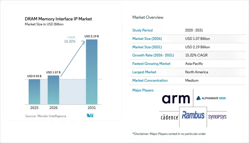
본 보고서는 메모리 인터페이스 아키텍처(DDR 및 DIMM 메모리 인터페이스 IP, LPDDR 메모리 인터페이스 IP, GDDR 메모리 인터페이스 IP, HBM 메모리 인터페이스 IP), 용도(데이터센터/클라우드/HPC/AI, 모바일 및 소비자 기기, 그래픽/게임 등), 고객 유형(팹리스 반도체 기업 등), 그리고 지역별로 분류되어 있습니다. 시장 전망은 금액(달러) 기준으로 제시되어 있습니다.
세계 DRAM 메모리 인터페이스 IP 시장 동향 및 인사이트
AI, HPC 및 데이터센터에서의 메모리 대역폭 요구 사항 증가
AI 훈련 및 추론 워크로드로 인해 메모리 대역폭은 첨단 가속기 설계의 핵심 제약 요인이 되고 있으며, DRAM 메모리 인터페이스 IP 시장의 전략적 역할이 커지고 있습니다. 사내 개발만으로는 경쟁 AI 프로그램의 일정을 따라잡을 수 없게 됨에 따라, 구매자들은 이미 실리콘 검증된 완전한 컨트롤러 및 PHY 스택을 점점 더 필요로 하고 있습니다. 이러한 요구 사항은 HBM 프로그램에서 특히 두드러집니다. HBM 프로그램에서는 서브시스템 검증, 패키징 준비 상태, 상호 운용성이 사후 작업이 아닌 구매 결정의 한 요소로 작용하고 있습니다. 이러한 추세로 인해 동적 랜덤 액세스 메모리(DRAM) 메모리 인터페이스 IP 시장에서 인증된 공급업체의 선택지는 점점 좁아지고 있습니다. 실적이 입증된 플랫폼을 통해 대규모 AI 및 HPC 도입을 지원할 수 있는 공급업체는 극소수에 불과하기 때문입니다. 시노프시스는 2026년 2월, 3nm 공정에서 9.2Gbps HBM4 IP 테스트 칩의 검증을 성공적으로 마쳤으며, 램버스는 2026년 3월, 핀당 최대 16Gbps를 지원하는 HBM4E 컨트롤러 IP를 출시했습니다. 이는 AI 메모리 요구 사항이 현재 제품 로드맵에 얼마나 큰 영향을 미치고 있는지를 보여줍니다.
LPDDR5X, GDDR7 및 HBM 연동 인터페이스로의 전환
LPDDR6, GDDR7 및 차세대 HBM으로의 전환에 따라, DRAM 메모리 인터페이스 IP 시장에서 모바일, 그래픽스, AI, 서버 각 분야에서 광범위한 교체 주기가 발생하고 있습니다. JEDEC은 2025년에 핀당 최대 14.4Gbps의 데이터 전송 속도와 더 넓은 대역폭의 채널 구조를 갖춘 LPDDR6 사양을 발표했습니다. 이는 공급업체가 최신 상태를 유지하기 위해서는 단순한 PHY의 사소한 개정 이상의 대응이 필요함을 의미합니다. Cadence사는 2025년 7월, LPDDR6/5X 14.4Gbps 메모리 IP 시스템 솔루션을 발표하며, 신규 규격의 채택과 상용 IP 제공을 직접 연계했습니다. 이러한 추세로 인해 DRAM 메모리 인터페이스 IP 시장의 벤더들은 여러 개발 트랙을 동시에 유지해야만 하게 되었으며, 연구 개발 압박이 커지는 한편, 보다 충실한 플랫폼 자원을 보유한 공급업체들이 유리한 입장에 서게 되었습니다. 또한, 많은 구매자들이 특정 규격의 전환기와 다음 전환기 사이에 끼이는 상황을 피하기 위해 차세대 IP를 조기에 확정하는 것을 선호하게 되면서, 고객의 일정에도 변화가 생기고 있습니다.
첨단 메모리 인터페이스의 고액 NRE 및 검증 비용
높은 개발 및 검증 비용은 특히 첨단 노드나 HBM 프로그램에서 DRAM 메모리 인터페이스 IP 시장에 여전히 가장 뚜렷한 걸림돌이 되고 있습니다. 기술적 부담은 컨트롤러나 PHY 설계에 그치지 않고, 패키지와 상호작용, 상호운용성 확보, 그리고 다양한 작동 조건에 걸친 상세한 특성 평가까지 미치고 있습니다. 시노프시스의 HBM4 검증에 대한 이정표와 GUC가 TSMC의 3nm 공정(CoWoS 채택)에서 선보인 12Gbps HBM4 데모는 상용화가 현실화되기까지 필요한 기술적 깊이를 보여줍니다. 이러한 비용 구조로 인해 최첨단 IP를 신속하게 도입할 수 있는 고객층이 좁아질 뿐만 아니라, 연속되는 규격에 걸친 개발에 자금을 투입할 수 있는 벤더의 선택지도 좁아집니다. 현실적으로 DRAM 메모리 인터페이스 IP 시장은 성장을 이어가고 있지만, 그 최고 가치 계층에 대한 접근은 소규모 신규 진출기업보다는 대형 벤더나 자금력이 있는 구매자에게 여전히 용이한 상황입니다.
부문 분석
2025년, DDR 및 DIMM 메모리 인터페이스 IP는 클라우드, 엔터프라이즈, AI 서버 시스템에서의 DDR5 및 MRDIMM 인터페이스의 광범위한 도입 실적을 바탕으로 DRAM 메모리 인터페이스 IP 시장 점유율의 39.21%를 차지했습니다. 서버 플랫폼이 익숙한 DDR 생태계를 포기하지 않으면서 메모리 대역폭 향상을 지속함에 따라, DRAM 메모리 인터페이스 IP 시장의 이 분야는 계속해서 호황을 누렸습니다. 2025년 4월, Cadence는 AI 클라우드 및 엔터프라이즈 데이터센터용 TSMC N3 공정을 기반으로 한 DDR5 12.8Gbps MRDIMM Gen2 메모리 IP 시스템 솔루션을 발표하며 이러한 수요를 더욱 부추겼습니다. 또한 LPDDR 역시 새로운 규격이 자동차 컴퓨팅, 엣지 AI, 저전력 서버 메모리 용도과 연계되면서, 휴대전화 이외의 분야에서도 그 중요성을 지속적으로 확대되고 있습니다.
JEDEC의 2025년판 LPDDR6 자료에서는 핀당 14.4Gbps로의 전환과 채널 구조의 확장이 제시되어, 모바일 및 추론 워크로드를 지원하는 공급업체들에게 새로운 개발 주기가 열렸습니다. Cadence는 이러한 전환에 발맞추어 LPDDR6/5X 시스템 솔루션을 발표하며, 표준 제정 움직임이 얼마나 신속하게 제품 출시로 이어지고 있는지를 보여주었습니다. HBM 메모리 인터페이스 IP는 2031년까지 연평균 성장률(CAGR) 16.12%를 나타낼 것으로 예측되며, AI 가속기 및 GPU 프로그램이 HBM4 및 HBM4E 주기로 전환됨에 따라 DRAM 메모리 인터페이스 IP 시장에서 가장 빠르게 성장하는 아키텍처가 될 전망입니다. 램버스(Lambus)는 2026년 3월에 HBM4E 컨트롤러 IP를 발표했으며, GUC는 2026년 4월에 12Gbps HBM4 플랫폼을 시연했습니다. 이는 HBM이 컨트롤러 로직, PHY 설계, 패키지 지원, 시뮬레이션 관련 자료 등을 포함하는 보다 광범위한 서브시스템으로서의 기회가 되고 있음을 보여줍니다.
지역별 분석
2025년, 북미는 DRAM 메모리 인터페이스 IP 시장 점유율의 39.51%를 차지하며, 지역별로는 가장 큰 기여도를 보였습니다. 이 지역은 하이퍼스케일러, AI 칩 개발 기업, 주요 플랫폼 IP 벤더가 밀집해 있다는 이점이 있어, 시장의 최첨단 분야에서 유례없이 활발한 설계 활동이 이루어지고 있습니다. 시노프시스, 케이던스, 램버스 등 각사는 HBM, DDR, LPDDR 플랫폼에서의 리더십을 통해 북미에서 시작된 고부가가치 파이프라인의 대부분을 계속해서 주도하고 있습니다. 또한, 북미의 프로젝트는 맞춤형 AI 실리콘이나 대규모 클라우드 인프라의 로드맵과 연계된 경우가 많아, 고부가가치이며 장기적인 계약으로 이어지는 경향이 있습니다. 따라서 구매 기업의 수는 제한적이지만, 이 지역의 DRAM 메모리 인터페이스 IP 시장은 특히 두터운 규모를 유지하고 있습니다.
유럽은 자동차용 반도체 수요와 안전성을 중시하는 인증 요건을 통해 독자적인 입지를 유지하고 있습니다. 이 지역의 자동차 부품 공급업체들은 차량용 대역폭 확대와 긴 제품 수명 주기라는 두 가지 요건을 모두 충족할 수 있는 메모리 인터페이스를 필요로 하고 있으며, 이것이 인증된 LPDDR 및 향후 GDDR 솔루션에 대한 지속적인 수요를 뒷받침하고 있습니다. JEDEC의 자동차용 가이드라인에서는 첨단 차량용 AI 시스템에 고성능 메모리가 필수적임을 명확히 보여주고 있으며, 한편으로 규정 준수 요구 사항은 여전히 엄격한 상태입니다. 또한 유럽은 첨단 패키징 워크플로우와 관련된 설계 및 검증 역량을 통해 공급 측면에서도 기여하고 있습니다. 지멘스 EDA의 HBM 패키징 지침은 메모리 인터페이스 계획이 시스템 및 패키지의 공동 설계와 점점 더 밀접하게 연결되어 있음을 보여주며, 직접 라이선싱 규모가 북미보다 작더라도 유럽이 기술 구현에서 수행하는 역할을 더욱 강화하고 있습니다.
아시아태평양은 2031년까지 연평균 성장률(CAGR) 16.28%를 나타낼 것으로 예측되며, DRAM 메모리 인터페이스 IP 시장에서 가장 두드러진 성장을 보일 것으로 전망됩니다. 대만과 한국은 첨단 패키징 및 HBM 생산이 이 시장에 집중되어 있어 여전히 중심적인 위치를 차지하고 있습니다. GUC가 TSMC의 3nm 공정과 CoWoS를 활용한 HBM4 시연을 통해, 최신 패키징 관련 메모리 인터페이스를 양산 단계로 한 걸음 더 가까이 끌어올리는 데 있어 대만이 수행하는 역할을 보여주고 있습니다. 또한 IP 공급 측면에서도 한국의 존재감이 커지고 있으며, OPENEDGES는 2026년 4월 LPDDR6 및 LPDDR5X 메모리 서브시스템 IP에 관한 첫 상용 라이선스 계약을 체결했습니다. 중국은 메모리 인터페이스 IP의 현지화를 추진하고 있으며, 2026년 1월 Innosilicon이 국내 최초로 LPDDR6 및 LPDDR5X 콤보 PHY와 컨트롤러를 납품한 것은 이러한 방향성에서 주목할 만한 한 걸음이 되었습니다. 일본은 자동차 및 산업용 수요를 통해 여전히 중요한 위치를 차지하고 있지만, 세계 기타 지역에서는 더 광범위한 아시아태평양공급망과 연계된 설계 서비스 및 통합 지원을 통해 시장이 서서히 확대되고 있습니다.
기타 혜택:
- 엑셀 형식 시장 예측(ME) 시트
- 3개월간의 애널리스트 지원
자주 묻는 질문
목차
제1장 서론
제2장 조사 방법
제3장 주요 요약
제4장 시장 구도
제5장 시장 규모와 성장 예측
제6장 경쟁 구도
제7장 시장 기회와 향후 전망
KTH 26.08.06According to Mordor Intelligence, the DRAM memory interface IP market size is projected to be USD 0.93 billion in 2025, USD 1.07 billion in 2026, and reach USD 2.19 billion by 2031, growing at a CAGR of 15.32% from 2026 to 2031.
This report is Segmented by Memory Interface Architecture (DDR and DIMM Memory Interface IP, LPDDR Memory Interface IP, GDDR Memory Interface IP, and HBM Memory Interface IP), Application (Data Center/Cloud/HPC/AI, Mobile and Consumer Devices, Graphics/Gaming, and More), Customer Type (Fabless Semiconductor Companies, and More), and Geography. The Market Forecasts are Provided in Terms of Value (USD).
Global DRAM Memory Interface IP Market Trends and Insights
Rising AI, HPC, and Data Center Memory Bandwidth Requirements
AI training and inference workloads have made memory bandwidth a central design constraint for advanced accelerators, elevating the strategic role of the DRAM memory interface IP market. Buyers increasingly need complete controller and PHY stacks that are already silicon-proven, because in-house development no longer aligns with the timing of competitive AI programs. That requirement is especially clear in HBM programs, where subsystem validation, packaging readiness, and interoperability have become part of the buying decision rather than follow-on work. This trend is tightening the qualified vendor pool in the dynamic random-access memory (DRAM) memory interface IP market, because only a few suppliers can support large AI and HPC deployments with proven platforms. Synopsys validated an HBM4 IP test chip at 9.2Gbps on a 3nm process in February 2026, and Rambus launched HBM4E controller IP rated up to 16Gbps per pin in March 2026, showing how strongly AI memory requirements are shaping current product roadmaps.
Migration To LPDDR5X, GDDR7, and HBM-Linked Interfaces
The move to LPDDR6, GDDR7, and newer HBM generations is creating a broad replacement cycle across mobile, graphics, AI, and server programs in the DRAM memory interface IP market. JEDEC presented LPDDR6 features in 2025 with data rates up to 14.4Gbps per pin and wider channel structures, which means suppliers need more than a minor PHY revision to stay current. Cadence launched an LPDDR6/5X 14.4Gbps memory IP system solution in July 2025, which linked new standard adoption directly to commercial IP availability. This pace is forcing vendors in the DRAM memory interface IP market to maintain multiple development tracks simultaneously, increasing R&D pressure and favoring suppliers with deeper platform resources. It also changes customer timing, because many buyers now prefer to lock in next-generation IP earlier to avoid getting trapped between one standard transition and the next.
High NRE and Validation Cost for Advanced Memory Interfaces
High development and validation costs remain the clearest brake on the DRAM memory interface IP market, especially at advanced nodes and in HBM programs. The technical burden now extends beyond controller and PHY design into package interaction, interoperability work, and deep characterization across multiple operating conditions. Synopsys's HBM4 validation milestone and GUC's 12Gbps HBM4 demonstration on TSMC's 3nm with CoWoS show the engineering depth required before commercial deployment becomes credible. That cost structure narrows the pool of customers that can quickly adopt the most advanced IP, and it also narrows the pool of vendors that can fund development across successive standards. In practical terms, the DRAM memory interface IP market continues to grow, but its highest-value tiers remain easier for large vendors and well-capitalized buyers to access than for smaller entrants.
Other drivers and restraints analyzed in the detailed report include:
- Increasing Chiplet-Based and Advanced Package Adoption
- Automotive ADAS and In-Vehicle Compute Memory Complexity
- Limited Customer Base and Long Qualification Cycles
For complete list of drivers and restraints, kindly check the Table Of Contents.
Segment Analysis
DDR and DIMM memory interface IP held 39.21% of the DRAM memory interface IP market share in 2025, supported by the broad installed base of DDR5 and MRDIMM interfaces in cloud, enterprise, and AI server systems. This part of the DRAM memory interface IP market remained active because server platforms continued to upgrade memory bandwidth without abandoning the familiar DDR ecosystem. Cadence reinforced that demand in April 2025 when it introduced a DDR5 12.8Gbps MRDIMM Gen2 memory IP system solution on TSMC N3 for AI cloud and enterprise data center deployments. LPDDR also continued to expand its relevance beyond handsets, as newer standards are now tied to automotive compute, edge AI, and low-power server memory applications.
JEDEC's 2025 LPDDR6 materials showed a move to 14.4 Gbps per pin and broader channel structures, opening a new development cycle for suppliers serving mobile and inference workloads. Cadence followed that transition with its LPDDR6/5X system solution, showing how quickly standards activity is translating into product launches. HBM memory interface IP is projected to grow at a 16.12% CAGR through 2031, making it the fastest-growing architecture in the DRAM memory interface IP market as AI accelerators and GPU programs move into HBM4 and HBM4E cycles. Rambus introduced HBM4E controller IP in March 2026, and GUC demonstrated a 12Gbps HBM4 platform in April 2026, which shows that HBM is becoming a broader subsystem opportunity that includes controller logic, PHY design, package support, and simulation collateral.
Complete Report Scope:
- By Memory Interface Architecture
- DDR and DIMM Memory Interface IP
- LPDDR Memory Interface IP
- GDDR Memory Interface IP
- HBM Memory Interface IP
- By Application
- Data Center/Cloud/HPC/AI
- Mobile and Consumer Devices
- Graphics/Gaming
- Automotive/ADAS
- Industrial/IoT/Networking
- By Customer Type
- Fabless Semiconductor Companies
- IDMs
- System OEMs
- Hyperscalers
- By Geography
- North America
- Europe
- Asia-Pacific
- China
- Japan
- South Korea
- Taiwan
- Rest of Asia-Pacific
- Rest of the World
Geography Analysis
North America held 39.51% of the DRAM memory interface IP market share in 2025, making it the largest regional contributor. The region benefits from a dense mix of hyperscalers, AI chip developers, and major platform IP vendors, which gives it unusually strong design activity at the advanced end of the market. Synopsys, Cadence, and Rambus continue to shape a large share of the high-value pipeline from North America through their leadership in HBM, DDR, and LPDDR platforms. North American programs also tend to support higher-value, longer-duration contracts because many are tied to custom AI silicon and large cloud infrastructure roadmaps. That keeps the DRAM memory interface IP market especially deep in this region, even when buyer counts remain limited.
Europe maintained a distinct position through automotive semiconductor demand and safety-driven qualification requirements. Automotive suppliers in the region need memory interfaces that can satisfy both higher in-vehicle bandwidth and long product life cycles, which support ongoing demand for qualified LPDDR and future GDDR solutions. JEDEC's automotive guidance makes clear that higher-performance memory is becoming necessary for advanced vehicle AI systems, while compliance expectations remain stringent. Europe also contributes to the supply side through design and verification capabilities linked to advanced packaging workflows. Siemens EDA's HBM packaging guidance shows how memory interface planning is increasingly tied to system and package co-design, which adds to Europe's role in enablement even when direct licensing scale is lower than in North America.
Asia-Pacific is projected to grow at a 16.28% CAGR through 2031, making it the fastest-growing geography in the DRAM memory interface IP market. Taiwan and South Korea remain central because advanced packaging and HBM production are heavily concentrated in these markets. GUC's HBM4 demonstration on TSMC 3nm with CoWoS reflects Taiwan's role in bringing the latest packaging-linked memory interfaces closer to production. South Korea is also becoming more visible on the IP supply side, as OPENEDGES signed its first commercial license for LPDDR6 and LPDDR5X memory subsystem IP in April 2026. China is pushing localization in memory interface IP, and Innosilicon's first domestic LPDDR6 and LPDDR5X combo PHY and controller delivery in January 2026 marked a notable step in that direction. Japan remains important through automotive and industrial demand, while the rest of the world continues to expand gradually through design services and integration support tied to the wider Asia-Pacific supply chain.
- Synopsys, Inc.
- Cadence Design Systems, Inc.
- Rambus Inc.
- Alphawave IP Group plc
- Arm Limited
- Siemens EDA
- Ansys, Inc.
- Silicon Creations, LLC
- VeriSilicon Microelectronics (Shanghai) Co., Ltd.
- Imagination Technologies Limited
- Broadcom Inc.
- Qualcomm Technologies, Inc.
- Marvell Technology, Inc.
- Intel Corporation
- Advanced Micro Devices, Inc.
- Samsung Electronics Co., Ltd.
- Micron Technology, Inc.
- SK hynix Inc.
- NXP Semiconductors N.V.
- Texas Instruments Incorporated
Additional Benefits:
- The market estimate (ME) sheet in Excel format
- 3 months of analyst support
TABLE OF CONTENTS
1 INTRODUCTION
- 1.1 Study Assumptions and Market Definition
- 1.2 Scope of the Study
2 RESEARCH METHODOLOGY
3 EXECUTIVE SUMMARY
4 MARKET LANDSCAPE
- 4.1 Market Overview
- 4.2 Market Drivers
- 4.2.1 Rising AI, HPC, and Data Center Memory Bandwidth Requirements
- 4.2.2 Migration to LPDDR5X, GDDR7, and HBM-Linked Interfaces
- 4.2.3 Increasing Chiplet-Based and Advanced Package Adoption
- 4.2.4 Automotive ADAS and In-Vehicle Compute Memory Complexity
- 4.2.5 Shorter Design Cycles Favoring Pre-Verified IP Reuse
- 4.2.6 Memory Security, Reliability, and Signal Integrity Demands
- 4.3 Market Restraints
- 4.3.1 High NRE and Validation Cost for Advanced Memory Interfaces
- 4.3.2 Limited Customer Base and Long Qualification Cycles
- 4.3.3 Rapid DRAM Standard Evolution Risking IP Obsolescence
- 4.3.4 Integration Complexity Across Process Nodes and Packages
- 4.4 Impact of Macroeconomic Factors on the Market
- 4.5 Industry Value Chain Analysis
- 4.6 Supply Chain Analysis
- 4.7 Regulatory Landscape
- 4.8 Technological Outlook
- 4.9 Porter's Five Forces Analysis
- 4.9.1 Threat of New Entrants
- 4.9.2 Bargaining Power of Suppliers
- 4.9.3 Bargaining Power of Buyers
- 4.9.4 Threat of Substitutes
- 4.9.5 Intensity of Competitive Rivalry
5 MARKET SIZE AND GROWTH FORECASTS (VALUE)
- 5.1 By Memory Interface Architecture
- 5.1.1 DDR and DIMM Memory Interface IP
- 5.1.2 LPDDR Memory Interface IP
- 5.1.3 GDDR Memory Interface IP
- 5.1.4 HBM Memory Interface IP
- 5.2 By Application
- 5.2.1 Data Center/Cloud/HPC/AI
- 5.2.2 Mobile and Consumer Devices
- 5.2.3 Graphics/Gaming
- 5.2.4 Automotive/ADAS
- 5.2.5 Industrial/IoT/Networking
- 5.3 By Customer Type
- 5.3.1 Fabless Semiconductor Companies
- 5.3.2 IDMs
- 5.3.3 System OEMs
- 5.3.4 Hyperscalers
- 5.4 By Geography
- 5.4.1 North America
- 5.4.2 Europe
- 5.4.3 Asia-Pacific
- 5.4.3.1 China
- 5.4.3.2 Japan
- 5.4.3.3 South Korea
- 5.4.3.4 Taiwan
- 5.4.3.5 Rest of Asia-Pacific
- 5.4.4 Rest of the World
6 COMPETITIVE LANDSCAPE
- 6.1 Market Concentration
- 6.2 Strategic Moves
- 6.3 Market Share Analysis
- 6.4 Company Profiles (includes Global Level Overview, Market Level Overview, Core Segments, Financials as available, Strategic Information, Market Rank/Share, Products and Services, Recent Developments)
- 6.4.1 Synopsys, Inc.
- 6.4.2 Cadence Design Systems, Inc.
- 6.4.3 Rambus Inc.
- 6.4.4 Alphawave IP Group plc
- 6.4.5 Arm Limited
- 6.4.6 Siemens EDA
- 6.4.7 Ansys, Inc.
- 6.4.8 Silicon Creations, LLC
- 6.4.9 VeriSilicon Microelectronics (Shanghai) Co., Ltd.
- 6.4.10 Imagination Technologies Limited
- 6.4.11 Broadcom Inc.
- 6.4.12 Qualcomm Technologies, Inc.
- 6.4.13 Marvell Technology, Inc.
- 6.4.14 Intel Corporation
- 6.4.15 Advanced Micro Devices, Inc.
- 6.4.16 Samsung Electronics Co., Ltd.
- 6.4.17 Micron Technology, Inc.
- 6.4.18 SK hynix Inc.
- 6.4.19 NXP Semiconductors N.V.
- 6.4.20 Texas Instruments Incorporated
7 MARKET OPPORTUNITIES AND FUTURE OUTLOOK
- 7.1 White-Space and Unmet-Need Assessment


