

|
시장보고서
상품코드
2099407
DRAM 패키징용 열전도성 인터페이스 재료 : 시장 점유율 분석, 업계 동향 및 통계, 성장 예측(2026-2031년)Thermal Interface Materials For DRAM Packaging - Market Share Analysis, Industry Trends & Statistics, Growth Forecasts (2026 - 2031) |
||||||
 Mordor Intelligence
Mordor Intelligence에 의하면, DRAM 패키징용 열전도성 인터페이스 재료 시장 규모는 2025년에 3억 9,000만 달러로 평가되었습니다. 2026년 4억 9,000만 달러에서 2031년까지 13억 2,000만 달러에 이를 것으로 예측되며, 2026년부터 2031년까지 CAGR은 21.92%를 나타낼 전망입니다.
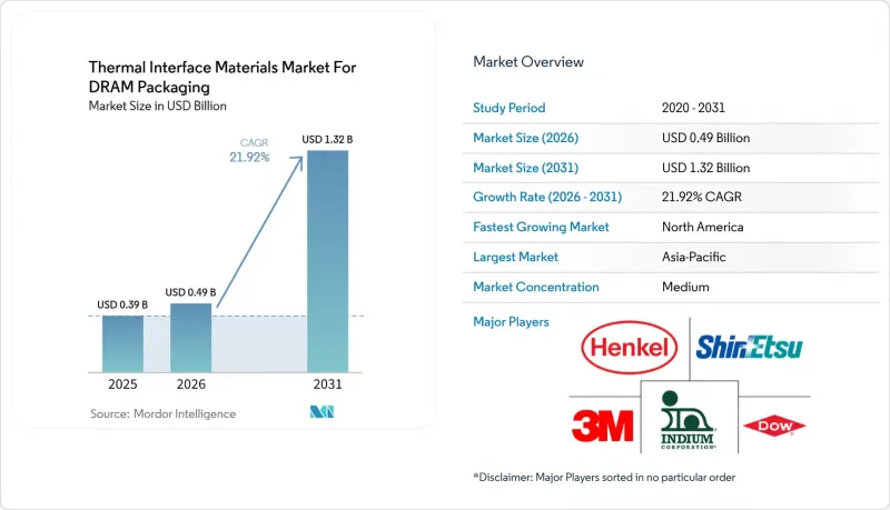
본 보고서는 소재 유형(열전도 그리스 및 페이스트, 열 패드/갭 패드 등), DRAM 패키지/제품 용도(HBM 스택, 첨단 DRAM 패키지, 서버용 DRAM 모듈 등), 최종 용도 플랫폼(AI 서버 및 가속기 등), 지역(북미 등)별로 분류되어 있습니다. 시장 전망은 금액(달러) 기준으로 제시되어 있습니다.
DRAM 패키징용 열전도성 인터페이스 재료 시장 인사이트 및 동향
HBM 스택의 높이 및 D2D 열 밀도 증가
DRAM 패키징용 열전도성 인터페이스 재료 시장은 더 많은 다이가 더 좁은 수직 공간 내에 배치되는 스택형 메모리 아키텍처의 부상에 직접 대응하고 있습니다. HBM 구조의 높이가 증가하면 하층 다이에서 패키지 리드까지의 직렬 열저항이 증가하여, 외부 냉각이 개선되더라도 열 제거가 어려워집니다. Siemens EDA는 HBM4의 설계 목표에서 스택 높이와 I/O 밀도가 모두 향상되어, 이로 인해 다이 간(D2D) 물리 계층에서 국부적인 열 집중이 증가할 것이라고 지적합니다. Imec은 2025년에 이 열적 과제의 규모를 제시하며, 열 대책을 시행하지 않은 3D HBM-on-GPU 구성에서는 GPU의 최고 온도가 141.7°C에 달하는 반면, 2.5D 기준 구성에서는 69.1°C에 그칩니다고 보고했습니다. 이에 반해 SK하이닉스는 2026년 5월, D2D PHY 영역에 냉각 요소를 통합한 iHBM 솔루션을 발표했습니다. 이를 통해 기존 시스템 인 패키지(SiP) 구조와의 호환성을 유지하면서 열 저항을 30% 저감하는 데 성공했습니다. 그 결과, DRAM 패키징 산업용 열계면재 시장은 패키지 내부의 여러 계면 위치에서 더 좁은 갭, 더 안정적인 본딩 라인, 그리고 더 높은 열전도율을 지원할 수 있는 소재로 전환되고 있습니다.
하이브리드 본딩으로의 전환과 열적 공동 최적화
DRAM 패키징용 열전도성 인터페이스 재료 시장은 첨단 메모리 어셈블리에서 열압축 본딩에서 하이브리드 구리 본딩으로의 전환에 따라 재편되고 있습니다. 이러한 전환으로 인해 열이 축적되는 위치와 재료 선택이 패키지의 무결성 및 열 성능 모두에 미치는 영향이 변화합니다. 2025년 『Electronics』지에 게재된 리뷰 기사에서는 SiCN 유전체, 나노트윈 구리 및 폴리머 복합재료가 열 저항, 뒤틀림 제어, 열팽창 계수의 불일치 측면에서 각각 상이한 절충점을 가져온다고 설명되었습니다. Imec의 기술 간 공동 최적화 연구에서는 기술 및 시스템 냉각에 관한 결정을 개별적으로가 아니라 통합적으로 모델링함으로써, 하이브리드 본딩된 3D 시스템이 2.5D의 열 거동에 가까워질 수 있음을 보여주었습니다. 이러한 발전에 따라 제품 수요는 스택 내부 소재와 리드 계면 소재라는 별개의 분야로 나뉘고 있으며, 그 결과 공급업체의 제품 포트폴리오는 더욱 전문화되고 있습니다. 실용적인 관점에서 볼 때, DRAM 패키징 업계의 열 계면 재료 시장에서는 단일 재료 선정에서 보다 광범위한 패키지 수준의 열 설계 결정으로 조달 방침이 전환되고 있습니다.
고기능 필러 및 수지 원료로 인한 비용 압박
DRAM 패키징용 열전도성 인터페이스 재료 시장은 고성능 배합에 사용되는 고급 충전제 및 실리콘계 캐리어 시스템으로 인한 뚜렷한 비용 압박에 직면해 있습니다. 신에츠 화학공업은 2026년 4월, 중동공급 상황에 기인한 원유 및 나프타 비용 상승을 이유로 모든 실리콘 제품의 가격을 10% 이상 인상한다고 발표했습니다. 이는 DRAM 패키징에서 실리콘계 시스템이 여전히 인증 재료 기반의 대부분을 차지하고 있기 때문에 중요한 의미를 지닙니다. 이러한 영향은 본드 라인이 얇은 분야에서 더욱 두드러집니다. 콤팩트한 형상에서 성능을 안정화하기 위해서는 고순도이며 엄격하게 관리된 필러 시스템이 필요하기 때문입니다. 대형 공급업체는 규모의 경제와 광범위한 조달 네트워크를 통해 이러한 압박의 일부를 흡수할 수 있지만, 중소규모의 배합 제조업체에게는 이익률을 지킬 여지가 제한적입니다. 그 결과, DRAM 패키징용 열전도성 인터페이스 재료 시장에서는 투입 비용의 상승이 기존 기업의 우위를 강화하는 한편, 차세대 제품에는 더욱 전문적인 원료가 요구되고 있습니다.
부문 분석
2025년, DRAM 패키징용 열전도성 인터페이스 재료 시장에서 써멀 패드/갭 패드는 34.67%의 점유율을 차지하며, 계속해서 주요 재료 카테고리로서의 지위를 유지했습니다. 이러한 확고한 입지는 서버용 DRAM 모듈 및 엔터프라이즈용 메모리 시스템에서의 확고한 사용에 기인하며, 이러한 분야에서는 일관된 본딩 라인 제어와 취급의 용이성이 여전히 중요시되고 있습니다. 또한, 이러한 제품은 자동 조립 공정에도 적합하며, 다른 몇 가지 대체 방식보다 리워크 요구 사항에 대응하기 쉽다는 장점도 있습니다. 이러한 조합 덕분에 패키징 요구 사항이 더욱 복잡해지는 상황에서도 패드 기반 제품은 기존 DRAM 모듈 조립의 중심적인 위치를 계속 차지하고 있습니다. DRAM 패키징 시장을 위한 열 인터페이스 재료는 여전히 최고 전도도와 마찬가지로 제조 용이성 및 인증 실적이 중시되는 이러한 형식에 의존하고 있습니다.
열 젤 및 디스펜서 호환 갭 필러는 2031년까지 연평균 성장률(CAGR) 22.15%를 나타낼 것으로 예측되며, 이는 HBM 스택 및 2.5D 인터포저 기반 패키지에서 더욱 정밀한 인터페이스 형상에 대한 높은 적합성을 반영합니다. 2026년 5월 다우(Dow)사가 ‘DOWSIL TC-3120 열전도 젤’을 출시한 것은 각 공급업체들이 오일 블리딩 및 응축성 아웃가스 발생이 적은 디스펜서용 소재를 고밀도·고속 전자기기용으로 포지셔닝하고 있음을 보여줍니다. 또한, 상변화 소재도 반복 사이클 중 펌프아웃 위험을 저감할 수 있어 리드 계면에서 채택이 확대되고 있습니다. 그리스나 페이스트는 기존 서버 플랫폼에서는 계속 사용되고 있지만, 본딩 라인의 편차나 마이그레이션 위험이 용납되기 어려운 첨단 노드에서는 그 채택이 점점 더 까다로워지고 있습니다. '기타' 카테고리는 현재 매출 규모 면에서 여전히 소규모이지만, 탄소계, 흑연계 및 기타 신소재가 표준 폴리머계로는 충분히 기능하지 못하는 인터페이스 부위에 대응할 가능성이 있어 주목받고 있습니다.
지역별 분석
2025년, 아시아태평양은 DRAM 패키징용 열전도성 인터페이스 재료 시장의 82.67%를 차지하며, 이 지역이 세계 수요의 중심지임이 명확해졌습니다. 이러한 집중 현상은 한국, 대만, 일본, 중국에 걸쳐 있는 DRAM 생산, HBM 조립 및 첨단 반도체 수탁 조립·테스트(OEM) 역량의 지리적 집적을 반영합니다. 한국은 여전히 가장 중요한 위치를 차지하고 있으며, 이는 Samsung Electronics 및 SK하이닉스가 대규모 HBM 생산 능력 외에도 차세대 패키지의 열 설계에 직접 관여하고 있기 때문입니다. SK하이닉스의 2026년 iHBM 출시는 이 지역의 메모리 제조업체들이 패키지 아키텍처와 그 주변 인터페이스 재료의 요구 사항을 어떻게 형성하고 있는지를 보여줍니다. 대만은 첨단 패키징 생태계를 통해 그 중요성이 더욱 커지고 있습니다. 이곳에서는 인터포저 기반 조립 및 코패키지 구조로 인해 관리가 필요한 열에 민감한 인터페이스의 수가 증가하고 있습니다.
일본은 고순도 소재 공급 및 메모리 관련 패키징 사업을 통해 DRAM 패키징용 열전도성 인터페이스 재료 시장을 뒷받침하고 있습니다. 한편, 중국은 국내 OSAT(수탁 패키징·조립) 기업의 성장과 현지화 노력을 통해 그 입지를 확대되고 있습니다. 동시에 아시아태평양에서는 일부 하이최종 용도, 특히 특수한 필러 시스템이나 낮은 아웃가스성이 요구되는 분야에서 여전히 수입된 고성능 배합 재료에 의존하고 있습니다. 북미 시장은 2031년까지 연평균 성장률(CAGR) 22.87%를 나타낼 것으로 예측되며, 지역별로는 가장 빠르게 성장하는 시장이 될 것입니다. 이러한 성장은 AI 인프라에 대한 투자, 하이퍼스케일러의 맞춤형 인증 수요, 그리고 국내 반도체 생산 능력에 대한 정책적 지원에 의해 주도되고 있습니다. 2026년 2월 카바이스(Carbis)와 다크 NX(Dark NX)간의 제휴, 그리고 2026년 4월 미국 해군과의 인증 계약은 북미 공급업체들이 높은 신뢰성과 용도 특화형 검증이 필요한 프리미엄 열 관리 분야를 목표로 하고 있음을 반영합니다.
북미 수요는 대규모 DRAM 다이 생산보다는 인증, 도입 및 성능 보증에 집중되어 있으며, 이로 인해 승인된 소재 하나당 부가가치가 높아지고 있습니다. 유럽은 DRAM 패키징용 열전도성 인터페이스 재료 시장에서 규모는 작지만 안정적인 점유율을 유지하고 있으며, 엔터프라이즈 데이터센터 수요와 특수 산업용 컴퓨팅 용도에 힘입고 있습니다. 유럽의 고객들은 규정 준수를 고려한 배합을 중시하며, 실리콘 프리 제품 및 저아웃가스 제품에 대한 관심은 여전히 높은 수준을 유지하고 있습니다. 세계 기타 지역은 여전히 매출 규모가 작지만, 동남아시아 국가들과 인도에서는 패키징 분야에 대한 관심이 높아지고 있으며, 지역 내 전자제품 제조가 확대됨에 따라 그 중요성이 커질 가능성이 있습니다.
기타 혜택 :
- 엑셀 형식 시장 예측(ME) 시트
- 3개월간의 애널리스트 지원
자주 묻는 질문
목차
제1장 서론
제2장 조사 방법
제3장 주요 요약
제4장 시장 구도
제5장 시장 규모 및 성장 예측
제6장 경쟁 구도
제7장 시장 기회 및 향후 전망
KTH 26.08.10According to Mordor Intelligence, the thermal interface materials market for DRAM packaging industry size was valued at USD 0.39 billion in 2025 and is estimated to grow from USD 0.49 billion in 2026 to reach USD 1.32 billion by 2031, at a CAGR of 21.92% during the forecast period 2026-2031.
This report is Segmented by Material Type (Thermal Greases and Pastes, Thermal Pads / Gap Pads, and More), DRAM Packaging / Product Application (HBM Stacks, Advanced DRAM Packages, Server DRAM Modules, and More), End-Use Platform (AI Servers and Accelerators, and More), and Geography (North America, and More). The Market Forecasts are Provided in Terms of Value (USD).
Insights and Trends of Thermal Interface Materials Market For DRAM Packaging
Rising HBM Stack Height and D2D Heat Density
The thermal interface materials market for DRAM packaging industry is responding directly to the rise in stacked memory architectures, where more dies are being placed within tighter vertical limits. Taller HBM structures increase serial thermal resistance from the lower dies to the package lid, which makes heat removal harder even when external cooling improves. Siemens EDA noted that HBM4 design targets raise both stack height and I/O density, which increases localized heat concentration in the die-to-die physical layer. Imec showed the scale of this thermal challenge in 2025, reporting a peak GPU temperature of 141.7°C in a 3D HBM-on-GPU setup without mitigation, versus 69.1°C in a 2.5D baseline. SK hynix responded in May 2026 by introducing its iHBM solution with integrated cooling elements in the D2D PHY area, which cut thermal resistance by 30% while staying compatible with existing System-in-Package structures. As a result, the thermal interface materials market for DRAM packaging industry is moving toward materials that can support tighter gaps, more stable bond lines, and higher conductivity at multiple interface positions inside the package.
Shift To Hybrid Bonding and Thermal Co-Optimization
The thermal interface materials market for DRAM packaging industry is also being reshaped by the move from thermal compression bonding toward hybrid copper bonding in advanced memory assembly. This shift changes where heat builds up and how material selection affects both package integrity and thermal performance. A 2025 review in Electronics described how SiCN dielectrics, nano-twinned copper, and polymer composites each bring different tradeoffs in thermal resistance, warpage control, and coefficient of thermal expansion mismatch. Imec's cross-technology co-optimization work showed that hybrid-bonded 3D systems can move closer to 2.5D thermal behavior when technology and system cooling decisions are modeled together, not in isolation. That development is splitting product demand into separate tracks for intra-stack materials and lid-interface materials, which makes supplier portfolios more specialized. In practical terms, the thermal interface materials market for DRAM packaging industry is seeing procurement shift from a single material decision toward a broader package-level thermal design decision.
Cost Pressure from Premium Filler And Resin Inputs
The thermal interface materials market for DRAM packaging industry faces clear cost pressure from premium fillers and silicone-based carrier systems used in high-performance formulations. Shin-Etsu announced in April 2026 that it would raise prices on all silicone products by 10% or more, citing crude oil and naphtha cost increases linked to Middle East supply conditions. That matters because silicone-based systems still account for much of the qualified material base in DRAM packaging. The effect is stronger in thinner bond lines, where high-purity and tightly controlled filler systems are needed to keep performance stable in compact geometries. Larger suppliers can absorb some of this pressure through scale and broader sourcing networks, while smaller formulators have less room to protect margins. As a result, the thermal interface materials market for DRAM packaging industry is seeing higher input costs reinforce incumbent strength at the same time that next-generation products require more specialized ingredients.
Other drivers and restraints analyzed in the detailed report include:
- Expansion of AI Server Memory Content Per System
- Reliability Requirements In 24/7 Enterprise Memory Systems
- Qualification Risk in Advanced DRAM Packaging Lines
For complete list of drivers and restraints, kindly check the Table Of Contents.
Segment Analysis
Thermal pads/gap pads held 34.67% of the thermal interface materials market for DRAM packaging industry share in 2025, which kept them as the leading material category. Their strong position came from established use in server DRAM modules and enterprise memory systems, where consistent bond-line control and easier handling remained valuable. They also fit well with automated assembly flows and support rework needs better than several alternative formats. That combination kept pad-based products central to conventional DRAM module assembly even as packaging demands became more complex. The thermal interface materials for DRAM packaging market still relies on these formats where manufacturability and qualification history matter as much as peak conductivity.
Thermal gels and dispensable gap fillers are forecast to grow at a 22.15% CAGR through 2031, reflecting their better fit with tighter interface geometries in HBM stacks and 2.5D interposer-based packages. Dow's launch of DOWSIL TC-3120 Thermal Gel in May 2026 showed how suppliers are positioning dispensable chemistries for dense, high-speed electronics with lower oil bleeding and lower condensed outgassing. Phase change materials are also gaining ground in lid-interface positions because they reduce pump-out risk during repeated cycling. Greases and pastes continue to serve conventional server platforms, but they face more pressure in advanced nodes where bond-line variation and migration risk are less acceptable. The Others category remains small in current revenue, yet it is drawing attention because carbon-based, graphite-based, and other novel materials could address interface positions that standard polymer systems serve less effectively.
Complete Report Scope:
- By Material Type
- Thermal Greases and Pastes
- Phase Change Materials
- Thermal Gels / Dispensable Gap Fillers
- Thermal Pads / Gap Pads
- Others (Graphite / Carbon-Based TIMs, Advanced Nano-Composite TIMs)
- By DRAM Packaging / Product Application
- HBM Stacks
- Advanced DRAM Packages
- Server DRAM Modules
- Client DRAM Modules
- CXL Attached DRAM Modules
- By End-Use Platform
- AI Servers and Accelerators
- High-Performance Computing
- Enterprise and Hyperscale Data Centers
- High-End Workstations
- Client PCs and Notebooks
- Industrial and Embedded Computing
- By Geography
- North America
- Europe
- Asia-Pacific
- China
- Japan
- South Korea
- Taiwan
- Rest of Asia-Pacific
- Rest of the World
Geography Analysis
Asia-Pacific held 82.67% of the thermal interface materials market for DRAM packaging industry market share in 2025, which made the region the clear center of global demand. This concentration reflects the geographic clustering of DRAM production, HBM assembly, and advanced outsourced semiconductor assembly and test capacity across South Korea, Taiwan, Japan, and China. South Korea remains the most important country position because Samsung Electronics and SK hynix combine large HBM output with direct involvement in next-generation package thermal design. SK hynix's 2026 iHBM launch shows how memory producers in the region are shaping both package architecture and the interface material requirements that sit around it. Taiwan adds further weight through its advanced packaging ecosystem, where interposer-based assembly and co-packaged structures increase the number of thermally sensitive interfaces that must be managed.
Japan supports the thermal interface materials market for DRAM packaging industry through high-purity materials supply and memory-related packaging operations, while China is expanding its position through domestic OSAT growth and localization efforts. At the same time, Asia-Pacific still depends on imported high-performance formulations in some premium applications, especially where specialized filler systems or low-outgassing behavior are required. North America is forecast to grow at a 22.87% CAGR through 2031, which makes it the fastest-rising regional market. This growth is being driven by AI infrastructure investment, custom qualification needs from hyperscalers, and policy support for domestic semiconductor capacity. Carbice's partnership with DarkNX in February 2026 and its U.S. Navy qualification contract in April 2026 reflect how North American suppliers are targeting premium thermal positions that require high reliability and application-specific validation.
Demand in North America is concentrated more in qualification, deployment, and performance assurance than in large-scale DRAM die production, which lifts value intensity per approved material. Europe remains a smaller but stable part of the thermal interface materials market for DRAM packaging industry, supported by enterprise data center demand and specialized industrial computing uses. European customers place greater emphasis on compliance-sensitive formulations, which keeps interest high in silicone-free and low-outgassing products. The Rest of the World remains a smaller revenue pool, but countries in Southeast Asia and India could add relevance as packaging ambitions grow and regional electronics manufacturing broadens.
- 3M
- Henkel AG and Co. KGaA
- The Dow Chemical Company
- Shin-Etsu Chemical Co., Ltd.
- Indium Corporation
- Parker-Hannifin Corporation
- Laird Thermal Systems, Inc.
- Henkel Adhesive Technologies
- Fujipoly, a division of Fuji Polymer Industries Co., Ltd.
- Momentive Performance Materials Inc.
- Boyd Corporation
- Momentive Technologies
- DuPont de Nemours, Inc.
- Wacker Chemie AG
- Honeywell International Inc.
- Saint-Gobain S.A.
- Aavid Thermalloy, LLC
- Wakefield-Vette, Inc.
- Carbice Corporation
- Fujipoly America Corporation
Additional Benefits:
- The market estimate (ME) sheet in Excel format
- 3 months of analyst support
TABLE OF CONTENTS
1 INTRODUCTION
- 1.1 Study Assumptions and Market Definition
- 1.2 Scope of the Study
2 RESEARCH METHODOLOGY
3 EXECUTIVE SUMMARY
4 MARKET LANDSCAPE
- 4.1 Market Overview
- 4.2 Impact of Macroeconomic Factors on the Market
- 4.3 Market Drivers
- 4.3.1 Rising HBM Stack Height and D2D Heat Density
- 4.3.2 Shift to Hybrid Bonding and Thermal Co-Optimization
- 4.3.3 Expansion of AI Server Memory Content Per System
- 4.3.4 Reliability Requirements in 24/7 Enterprise Memory Systems
- 4.3.5 High Thermal Conductivity Demand in Ultra-Thin Interface Gaps
- 4.3.6 Qualification of Silicone-Free and Low-Outgassing TIM Formulations
- 4.4 Market Restraints
- 4.4.1 Cost Pressure from Premium Filler and Resin Inputs
- 4.4.2 Qualification Risk in Advanced DRAM Packaging Lines
- 4.4.3 Substrate Warpage and Process Window Narrowing
- 4.4.4 Competition from Integrated Cooling and Package-Level Thermal Designs
- 4.5 Industry Value Chain Analysis
- 4.6 Regulatory Landscape
- 4.7 Technological Outlook
- 4.8 Porter's Five Forces Analysis
- 4.8.1 Bargaining Power of Suppliers
- 4.8.2 Bargaining Power of Buyers
- 4.8.3 Threat of New Entrants
- 4.8.4 Threat of Substitutes
- 4.8.5 Competitive Rivalry
5 MARKET SIZE AND GROWTH FORECASTS (VALUE)
- 5.1 By Material Type
- 5.1.1 Thermal Greases and Pastes
- 5.1.2 Phase Change Materials
- 5.1.3 Thermal Gels / Dispensable Gap Fillers
- 5.1.4 Thermal Pads / Gap Pads
- 5.1.5 Others (Graphite / Carbon-Based TIMs, Advanced Nano-Composite TIMs)
- 5.2 By DRAM Packaging / Product Application
- 5.2.1 HBM Stacks
- 5.2.2 Advanced DRAM Packages
- 5.2.3 Server DRAM Modules
- 5.2.4 Client DRAM Modules
- 5.2.5 CXL Attached DRAM Modules
- 5.3 By End-Use Platform
- 5.3.1 AI Servers and Accelerators
- 5.3.2 High-Performance Computing
- 5.3.3 Enterprise and Hyperscale Data Centers
- 5.3.4 High-End Workstations
- 5.3.5 Client PCs and Notebooks
- 5.3.6 Industrial and Embedded Computing
- 5.4 By Geography
- 5.4.1 North America
- 5.4.2 Europe
- 5.4.3 Asia-Pacific
- 5.4.3.1 China
- 5.4.3.2 Japan
- 5.4.3.3 South Korea
- 5.4.3.4 Taiwan
- 5.4.3.5 Rest of Asia-Pacific
- 5.4.4 Rest of the World
6 COMPETITIVE LANDSCAPE
- 6.1 Market Concentration
- 6.2 Strategic Moves
- 6.3 Market Share Analysis
- 6.4 Company Profiles (includes Global Level Overview, Market Level Overview, Core Segments, Financials as available, Strategic Information, Market Rank/Share, Products and Services, Recent Developments)
- 6.4.1 3M
- 6.4.2 Henkel AG and Co. KGaA
- 6.4.3 The Dow Chemical Company
- 6.4.4 Shin-Etsu Chemical Co., Ltd.
- 6.4.5 Indium Corporation
- 6.4.6 Parker-Hannifin Corporation
- 6.4.7 Laird Thermal Systems, Inc.
- 6.4.8 Henkel Adhesive Technologies
- 6.4.9 Fujipoly, a division of Fuji Polymer Industries Co., Ltd.
- 6.4.10 Momentive Performance Materials Inc.
- 6.4.11 Boyd Corporation
- 6.4.12 Momentive Technologies
- 6.4.13 DuPont de Nemours, Inc.
- 6.4.14 Wacker Chemie AG
- 6.4.15 Honeywell International Inc.
- 6.4.16 Saint-Gobain S.A.
- 6.4.17 Aavid Thermalloy, LLC
- 6.4.18 Wakefield-Vette, Inc.
- 6.4.19 Carbice Corporation
- 6.4.20 Fujipoly America Corporation
7 MARKET OPPORTUNITIES AND FUTURE OUTLOOK
- 7.1 White-Space and Unmet-Need Assessment


