

|
시장보고서
상품코드
2115921
SRAM 및 ROM 설계용 IP : 시장 점유율 분석, 산업 동향 및 통계 데이터, 성장 예측(2026-2031년)SRAM And ROM Design IP - Market Share Analysis, Industry Trends & Statistics, Growth Forecasts (2026 - 2031) |
||||||
 Mordor Intelligence
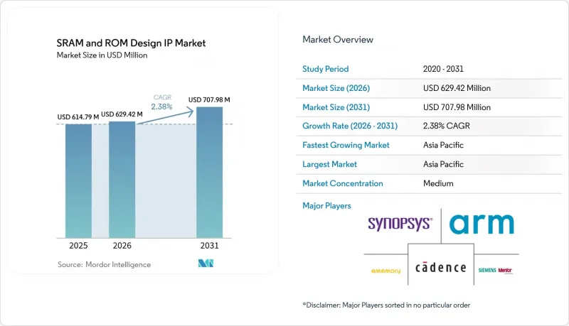
Mordor Intelligence에 의하면, SRAM 및 ROM 설계용 IP 시장 규모는 2025년에 6억 1,479만 달러로 평가되었습니다. 2026년 6억 2,942만 달러에서 2031년까지 7억 798만 달러에 이를 것으로 예상되며, 예측 기간(2026-2031년) CAGR은 2.38%를 나타낼 전망입니다.
본 보고서는 메모리 유형(SRAM, ROM, 기타), 용도(소비자용 전자기기, 통신·네트워크, 기타), 기술 노드(14nm 이하, 15-22nm, 28-40nm, 45nm 이상), IP 제공 방식(하드 IP, 소프트 IP, 기타),및 지역(북미, 남미, 유럽, 아시아태평양, 중동 및 아프리카)별로 분류되어 있습니다. 시장 예측은 금액(달러) 기준으로 제시되어 있습니다.
세계의 SRAM 및 ROM 설계용 IP 시장 동향 및 인사이트
대규모 온칩 캐시가 필요한 AI 중심 SoC의 보급
현재 추론 가속기에는 가중치나 특징 맵을 저장하기 위해 최대 40MB에 달하는 SRAM이 통합되어 있으며, 이는 범용 프로세서에서 볼 수 있는 8-16MB를 훨씬 상회합니다. ‘컴퓨트 인 메모리(Compute-in-Memory)’ 방식에서는 데이터 마이그레이션에 따른 에너지 소비를 줄이기 위해 산술 연산을 비트셀 내에 직접 배치하고 있으며, 이로 인해 컴파일러에 대한 새로운 요구 사항이 대두되고 있습니다. 또한, 여러 지역에서 추진되고 있는 ‘소버린 AI’ 이니셔티브는 현지에서 검증된 메모리 IP의 사용을 필수로 하는 국내 칩 개발 프로그램에 자금을 지원함으로써 시장 규모를 확대되고 있습니다. 3차원 적층형 실리콘 관통 비아(TSV)는 실적를 유지하면서 캐시의 상한선을 더욱 높여줍니다. 멀티 기가헤르츠에서 누설 전류가 낮은 SRAM 매크로를 종합적인 타이밍 코너와 함께 공급할 수 있는 벤더야말로 이러한 호황을 최대한 활용할 수 있는 위치에 있습니다.
5G 및 엣지 컴퓨팅의 확산이 저전력 임베디드 SRAM의 채택을 가속화하고 있습니다.
엣지 서버 및 IoT 노드에는 -40°C에서 125°C의 온도 범위에서 데이터를 유지할 수 있는 1V 미만의 메모리 블록이 요구됩니다. 차세대 IP에서는 멀티 스로숄드 트랜지스터와 파워 게이팅 셀을 결합하여 메가비트당 누설 전류를 1나노암페어 미만으로 억제하고 있습니다. 다이나믹 바디 바이어싱을 통해 설계자는 분 단위로 대기 전력 및 액세스 속도의 균형을 조정할 수 있게 됩니다. 이와 동시에, 5G 베이스밴드 ASIC에서는 버스트 패킷 버퍼링을 위해 미세 조정된 듀얼 포트 SRAM이 채택되고 있습니다. 이러한 엄격한 전력 프로파일은 특성 평가의 깊이와 코너 검증 기준을 높이며, 여러 파운드리에서 실리콘 검증 데이터를 보유한 공급업체에 유리하게 작용합니다.
오픈소스 메모리 컴파일러로 인한 가격 압박으로 평균 판매 가격(ASP) 하락
RISC-V 생태계와 관련된 커뮤니티 프로젝트에서는 현재 성숙한 노드를 위한 무료 SRAM 생성기를 제공하고 있으며, 비용에 민감한 웨어러블 기기 및 장난감 시장에서 상용 제품보다 저렴한 대안이 되고 있습니다. 대학들도 라이브러리 개발에 더욱 기여하고 있어, 팹리스 기업 팀이 신속하게 첫 실리콘을 구현할 수 있도록 지원하고 있습니다. 각 벤더들은 오픈소스 흐름에서 종종 누락되는 누설 전류 감소, 코너 커버리지, 안전 조치 패키지를 강조함으로써 수익성을 지키려 하고 있습니다. 그럼에도 불구하고, 엔트리 레벨의 수익원은 계속해서 축소되는 추세입니다.
부문별 분석
2025년, SRAM은 SRAM 및 ROM 설계용 IP 시장에서 60.05%의 점유율을 유지했습니다. 이는 캐시나 버퍼로서의 역할에서 SRAM이 타의 추종을 불허하는 속도를 발휘하고 있음을 보여줍니다. AI 가속기 및 5G 스위치가 더 대용량의 온다이 슬라이스를 필요로 함에 따라, 이 부문의 절대 금액은 완만하게 증가하고 있습니다. 한편, PROM, EPROM, EEPROM을 포함한 ROM 제품군은 부트 코드나 보정 테이블로 기능하고 있지만, 시스템 온 칩(SoC)의 집적화로 인해 개별 블록이 제거됨에 따라 그 규모는 점차 축소되고 있습니다. MRAM 및 기타 새로 등장한 비휘발성 메모리와 관련된 SRAM 및 ROM 설계용 IP 시장 규모는 여전히 소규모이지만, eFlash가 28nm 이하에서 용량 한계에 도달하면 그 입지는 강화될 전망입니다.
라이선싱은 임베디드 플래시 및 대체 비휘발성 메모리(NVM)와 관련이 있으며, IoT 마이크로컨트롤러와 자동차용 ECU가 내구성이 높은 코드 스토리지를 필요로 하기 때문에 연평균 성장률(CAGR) 3.72%라는 가장 빠른 속도로 성장하고 있습니다. SRAM의 속도와 MRAM의 비휘발성을 결합한 멀티테크놀로지 컴파일러는 시험 생산 단계에 접어든 하이브리드 어레이를 뒷받침하고 있습니다. 두 휘발성 도메인 모두에 정통한 벤더는 특히 공정 간에 동일한 논리 인터페이스를 매핑하여 펌웨어 이식 위험을 줄일 수 있는 경우, 가격 면에서 프리미엄을 확보하고 있습니다.
2025년에는 점점 더 정교한 그래픽과 로컬 AI 기능을 필요로 하는 스마트폰, 태블릿, 게임기를 주축으로, 소비자 가전제품이 SRAM 및 ROM용 설계 IP 시장 점유율의 36.10%를 차지했습니다. 설계 주기는 여전히 활발하지만, 벤더들이 카메라나 안테나를 위해 기판 공간을 재사용하고 있어 용량 증가는 정체 상태에 있습니다. 통신용 ASIC은 라인 레이트의 패킷 전송을 유지하기 위해 1나노초 미만의 지연 시간에 최적화된 듀얼 포트 SRAM에 의존하고 있으며, 이 틈새 시장에서는 컴파일러의 유연성이 높이 평가됩니다.
자동차 및 운송 기계 분야의 IP 수주액은 ASIL-D 진단 기능을 갖춘 수 기가바이트 규모의 온칩 어레이가 필요한 첨단 운전자 지원 시스템(ADAS) 수요에 힘입어 2031년까지 연평균 성장률(CAGR) 4.9%로 증가할 것으로 예측됩니다. 따라서, 그레이드 1 기능 안전 요구 사항을 준수하는 SRAM 및 ROM용 설계 IP 시장 규모는 다른 어떤 분야보다 빠르게 확대되고 있습니다. 항공우주 및 방위 분야 수요는 여전히 소량에 그치고 있지만, 내방사선 라이브러리는 엄격한 인증 절차를 거치기 때문에 평균 판매 가격이 높습니다.
지역별 분석
아시아태평양은 2025년 SRAM 및 ROM 설계용 IP 시장 매출의 46.85%를 차지했으며, 2031년까지 연평균 성장률(CAGR) 3.82%를 나타낼 것으로 예측됩니다. 대만, 한국, 중국 본토의 파운드리 클러스터가 테이프아웃 비용을 절감하는 한편, 각국의 보조금 제도가 국산 컴파일러 개발 프로젝트를 지원하고 있습니다. 일본은 Tier 1 자동차 부품 공급업체 및 산업용 로봇용으로 맞춤화된, 안전성에 중점을 둔 매크로를 제공하며 사업 영역을 넓히고 있습니다.
북미는 실리콘밸리의 스타트업과 하이퍼스케일 클라우드 벤더들이 독자적인 AI 칩 출시를 놓고 경쟁하는 가운데, 최첨단 설계 착수 건수의 대부분을 차지하고 있습니다. ‘CHIPS법’은 국내 팹에 새로운 자본을 유치하고, 국내 IP 검증 연구소 설립을 촉진하는 동시에 중소규모 기업을 위한 보조금 제공 경로를 개척하고 있습니다. 디트로이트의 자동차 Tier 1 공급업체는 항공우주 업계의 주요 기업과 제휴하여, 내방사선성이며 ASIL-D를 준수하는 매크로를 요구함으로써 고수익의 틈새 시장을 개척하고 있습니다.
유럽은 독일의 OEM 생태계와 ISO 26262의 엄격한 시행을 활용하여 자동차 및 산업용 자동화에 주력하고 있습니다. 북유럽 국가들은 가혹한 환경에 적합한 초저전력 메모리를 공급하는 한편, 프랑스와 이탈리아는 자국의 IP를 우선시하는 주권 컴퓨팅(sovereign computing) 이니셔티브를 모색하고 있습니다. 전반적으로 유럽 대륙 수요는 단순한 집적 밀도보다 신뢰성 및 기능 안전성 인증을 중시하는 경향을 보이고 있습니다.
기타 혜택 :
- 엑셀 형식 시장 예측(ME) 시트
- 3개월간의 애널리스트 지원
자주 묻는 질문
목차
제1장 서론
제2장 분석 방법
제3장 개요
제4장 시장 구도
제5장 시장 규모 및 성장률 예측
제6장 경쟁 구도
제7장 시장 기회 및 향후 전망
KTH 26.08.31According to Mordor Intelligence, the SRAM and ROM Design IP market size was valued at USD 614.79 million in 2025 and estimated to grow from USD 629.42 million in 2026 to reach USD 707.98 million by 2031, at a CAGR of 2.38% during the forecast period (2026-2031).
This report is Segmented by Memory Type (SRAM, ROM, and More), Application (Consumer Electronics, Telecommunications and Networking, and More), Technology Node (<=14nm, 15-22nm, 28-40nm, and >=45nm), IP Delivery Type (Hard IP, Soft IP, and More), and Geography (North America, South America, Europe, Asia Pacific, Middle East, and Africa). The Market Forecasts are Provided in Terms of Value (USD).
Global SRAM And ROM Design IP Market Trends and Insights
Proliferation of AI-centric SoCs demanding large on-chip cache
Inference accelerators now integrate as much as 40 MB of SRAM to store weights and feature maps, far eclipsing the 8-16 MB found in general-purpose processors. Compute-in-memory variants place arithmetic operations directly inside the bit cell to reduce data movement energy, creating new compiler requirements. Sovereign-AI initiatives in multiple regions add volume by funding domestic chip programs that insist on locally verified memory IP. Three-dimensional stacking through-silicon vias further raises cache ceilings while preserving the footprint. Vendors capable of shipping multi-gigahertz, low-leakage SRAM macros with exhaustive timing corners are best positioned to capitalize on this upswing.
5G and edge-computing roll-outs accelerating low-power embedded SRAM adoption
Edge servers and IoT nodes require sub-1V memory blocks that retain data across a temperature range of -40 °C to 125 °C. Next-generation IP now posts leakage below one nanoampere per megabit by combining multi-threshold transistors with power-gating cells. Dynamic body-biasing allows designers to trade standby power for access speed on a minute-to-minute basis. In parallel, 5G baseband ASICs rely on dual-port SRAM that is finely tuned for burst packet buffering. These stringent power profiles raise the bar for characterization depth and corner validation, favoring suppliers with silicon-proven data across multiple foundries.
Pricing pressure from open-source memory compilers eroding ASPs
Community projects tied to the RISC-V ecosystem now deliver free SRAM generators for mature nodes, undercutting commercial offerings in cost-sensitive wearables and toys. Universities further seed libraries, giving fabless teams a quick path to first silicon. Vendors defend their margins by emphasizing the reduction of leakage, coverage of corners, and safety packages that open-source flows often lack. Nonetheless, entry-level revenue streams continue to compress.
Other drivers and restraints analyzed in the detailed report include:
- Transition from eFlash to MRAM below 28 nm unlocking new licensing revenue streams
- Automotive Grade-1 functional-safety rules boosting qualified memory IP demand
- Export-control compliance hurdles for Chinese tape-outs
For complete list of drivers and restraints, kindly check the Table Of Contents.
Segment Analysis
SRAM retained 60.05% share of the SRAM and ROM Design IP market in 2025, a testament to its unmatched speed in cache and buffer roles. The segment climbs modestly in absolute dollars as AI accelerators and 5G switches request fatter on-die slices. In parallel, ROM families, including PROM, EPROM, and EEPROM, serve as boot code and calibration tables, but gradually shrink as system-on-chip consolidation removes discrete blocks. The SRAM and ROM Design IP market size associated with MRAM and other non-volatile newcomers remains modest, yet their position strengthens once eFlash reaches a capacity limit below 28 nm.
Licensing tied to embedded flash and alternative NVM grows at the fastest rate, with a 3.72% CAGR, because IoT microcontrollers and automotive ECUs require durable code storage. Multi-technology compilers that couple SRAM's speed with MRAM's persistence underpin hybrid arrays entering pilot production. Vendors versed in both volatility domains command a pricing premium, especially when they can map identical logical interfaces across processes, trimming firmware porting risk.
Consumer devices held 36.10% of the SRAM and ROM Design IP market share in 2025, driven by smartphones, tablets, and consoles that demand ever-richer graphics and local AI capabilities. Design cycles remain brisk, but capacity gains plateau as vendors recycle board real estate for cameras and antennas. Telecommunications ASICs rely on dual-port SRAM tuned for <1 ns latency to maintain line-rate packet forwarding, a niche that rewards compiler flexibility.
Automotive and transportation IP bookings are projected to rise at a 4.9% CAGR to 2031, driven by the demand for advanced driver-assistance systems that require multi-gigabyte on-chip arrays paired with ASIL-D diagnostics. The SRAM and ROM Design IP market size exposed to Grade-1 functional safety, therefore, increases faster than any other vertical. Aerospace and defense requests remain small in volume, yet they yield high average selling prices because radiation-hardened libraries undergo rigorous qualification.
Complete Report Scope:
- By Memory Type
- SRAM
- ROM (PROM / EPROM / EEPROM)
- MRAM
- Embedded Flash / Other NVM
- By Application
- Consumer Electronics
- Telecommunications and Networking
- Automotive and Transportation
- Industrial and IoT
- Aerospace and Defense
- Other Applications
- By Technology Node
- <=14 nm
- 15 - 22 nm
- 28 - 40 nm
- >=45 nm
- By IP Delivery Type
- Hard IP
- Soft IP
- Parameterised Compiler IP
- Chiplet / 3D Die-level IP
- By Geography
- North America
- United States
- Canada
- Mexico
- South America
- Brazil
- Argentina
- Rest of South America
- Europe
- Germany
- United Kingdom
- France
- Italy
- Spain
- Rest of Europe
- Asia Pacific
- China
- Japan
- India
- South Korea
- South-East Asia
- Rest of Asia Pacific
- Middle East
- Saudi Arabia
- United Arab Emirates
- Turkey
- Rest of Middle East
- Africa
- South Africa
- Nigeria
- Rest of Africa
- North America
Geography Analysis
The Asia Pacific held 46.85% of the SRAM and ROM Design IP market revenue in 2025 and is projected to grow at a 3.82% CAGR through 2031. Foundry clusters in Taiwan, South Korea, and mainland China lower tape-out costs, while national subsidy schemes bankroll indigenous compiler projects. Japan contributes safety-focused macros tailored for Tier-1 automotive suppliers and industrial robotics, reinforcing regional breadth.
North America commands the lion's share of bleeding-edge design starts as Silicon Valley startups and hyperscale cloud vendors race to release proprietary AI silicon. The CHIPS Act funnels fresh capital into domestic fabs, catalyzing on-shore IP verification labs and opening grant channels for smaller houses. Automotive Tier-1s in Detroit partner with aerospace primes to request radiation-hard, ASIL-D compliant macros, tapping into high-margin niches.
Europe focuses on automotive and industrial automation, leveraging Germany's OEM ecosystem and stringent enforcement of ISO 26262. Nordic countries supply ultra-low-power memories for harsh environments, while France and Italy explore sovereign computing initiatives that favor local IP. Overall, continental demand tilts toward reliability and functional safety credentials over raw density.
- Arm Ltd.
- Synopsys Inc.
- Cadence Design Systems Inc.
- Siemens EDA (Mentor Graphics Corporation)
- eMemory Technology Inc.
- Silvaco Inc.
- Dolphin Design SAS
- VeriSilicon Holdings Co. Ltd.
- SureCore Ltd.
- Xilinx Inc.
- Renesas Electronics Corporation
- Everspin Technologies Inc.
- Avalanche Technology Inc.
- TDK Corporation
- Kilopass Technology Inc.
- Silicon Storage Technology Inc.
- GSI Technology Inc.
- Dolphin Technology Inc.
- TekStart LLC
- Flex Logix Technologies Inc.
- Rambus Inc.
Additional Benefits:
- The market estimate (ME) sheet in Excel format
- 3 months of analyst support
TABLE OF CONTENTS
1 INTRODUCTION
- 1.1 Study Assumptions and Market Definition
- 1.2 Scope of the Study
2 RESEARCH METHODOLOGY
3 EXECUTIVE SUMMARY
4 MARKET LANDSCAPE
- 4.1 Market Overview
- 4.2 Market Drivers
- 4.2.1 Proliferation of AI-centric SoCs demanding large on-chip cache
- 4.2.2 5G and edge-computing roll-outs accelerating low-power embedded SRAM adoption
- 4.2.3 Transition from eFlash to MRAM below 28 nm unlocking new licensing revenue streams
- 4.2.4 Automotive Grade-1 functional-safety rules boosting qualified memory IP demand
- 4.2.5 Chiplet architectures standardising die-to-die memory IP requirements
- 4.2.6 Foundry turnkey memory-compiler programs shortening time-to-market for fabless firms
- 4.3 Market Restraints
- 4.3.1 Pricing pressure from open-source memory compilers eroding ASPs
- 4.3.2 Emerging ReRAM/FeRAM alternatives cannibalising small ROM IP sockets
- 4.3.3 Export-control compliance hurdles for Chinese tape-outs
- 4.3.4 Reliability headwinds for ?7 nm SRAM bit-cells inflating qualification cost
- 4.4 Industry Ecosystem Analysis
- 4.5 Impact of Macroeconomic Factors
- 4.6 Technological Outlook
- 4.7 Porter's Five Forces Analysis
- 4.7.1 Threat of New Entrants
- 4.7.2 Bargaining Power of Suppliers
- 4.7.3 Bargaining Power of Buyers
- 4.7.4 Threat of Substitutes
- 4.7.5 Competitive Rivalry
5 MARKET SIZE AND GROWTH FORECASTS (VALUE)
- 5.1 By Memory Type
- 5.1.1 SRAM
- 5.1.2 ROM (PROM / EPROM / EEPROM)
- 5.1.3 MRAM
- 5.1.4 Embedded Flash / Other NVM
- 5.2 By Application
- 5.2.1 Consumer Electronics
- 5.2.2 Telecommunications and Networking
- 5.2.3 Automotive and Transportation
- 5.2.4 Industrial and IoT
- 5.2.5 Aerospace and Defense
- 5.2.6 Other Applications
- 5.3 By Technology Node
- 5.3.1 <=14 nm
- 5.3.2 15 - 22 nm
- 5.3.3 28 - 40 nm
- 5.3.4 >=45 nm
- 5.4 By IP Delivery Type
- 5.4.1 Hard IP
- 5.4.2 Soft IP
- 5.4.3 Parameterised Compiler IP
- 5.4.4 Chiplet / 3D Die-level IP
- 5.5 By Geography
- 5.5.1 North America
- 5.5.1.1 United States
- 5.5.1.2 Canada
- 5.5.1.3 Mexico
- 5.5.2 South America
- 5.5.2.1 Brazil
- 5.5.2.2 Argentina
- 5.5.2.3 Rest of South America
- 5.5.3 Europe
- 5.5.3.1 Germany
- 5.5.3.2 United Kingdom
- 5.5.3.3 France
- 5.5.3.4 Italy
- 5.5.3.5 Spain
- 5.5.3.6 Rest of Europe
- 5.5.4 Asia Pacific
- 5.5.4.1 China
- 5.5.4.2 Japan
- 5.5.4.3 India
- 5.5.4.4 South Korea
- 5.5.4.5 South-East Asia
- 5.5.4.6 Rest of Asia Pacific
- 5.5.5 Middle East
- 5.5.5.1 Saudi Arabia
- 5.5.5.2 United Arab Emirates
- 5.5.5.3 Turkey
- 5.5.5.4 Rest of Middle East
- 5.5.6 Africa
- 5.5.6.1 South Africa
- 5.5.6.2 Nigeria
- 5.5.6.3 Rest of Africa
- 5.5.1 North America
6 COMPETITIVE LANDSCAPE
- 6.1 Market Concentration
- 6.2 Strategic Moves
- 6.3 Market Share Analysis
- 6.4 Company Profiles (includes Global level Overview, Market level overview, Core Segments, Financials as available, Strategic Information, Market Rank/Share for key companies, Products and Services, and Recent Developments)
- 6.4.1 Arm Ltd.
- 6.4.2 Synopsys Inc.
- 6.4.3 Cadence Design Systems Inc.
- 6.4.4 Siemens EDA (Mentor Graphics Corporation)
- 6.4.5 eMemory Technology Inc.
- 6.4.6 Silvaco Inc.
- 6.4.7 Dolphin Design SAS
- 6.4.8 VeriSilicon Holdings Co. Ltd.
- 6.4.9 SureCore Ltd.
- 6.4.10 Xilinx Inc.
- 6.4.11 Renesas Electronics Corporation
- 6.4.12 Everspin Technologies Inc.
- 6.4.13 Avalanche Technology Inc.
- 6.4.14 TDK Corporation
- 6.4.15 Kilopass Technology Inc.
- 6.4.16 Silicon Storage Technology Inc.
- 6.4.17 GSI Technology Inc.
- 6.4.18 Dolphin Technology Inc.
- 6.4.19 TekStart LLC
- 6.4.20 Flex Logix Technologies Inc.
- 6.4.21 Rambus Inc.
7 MARKET OPPORTUNITIES AND FUTURE OUTLOOK
- 7.1 White-space and Unmet-Need Assessment


