|
시장보고서
상품코드
2122304
프로그래머블 ASIC 시장 : 시장 점유율 분석, 업계 동향 및 통계, 성장 예측(2026-2031년)Programmable ASIC - Market Share Analysis, Industry Trends & Statistics, Growth Forecasts (2026 - 2031) |
||||||
 Mordor Intelligence
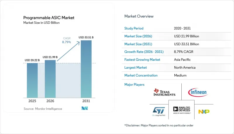
Mordor Intelligence에 의하면, 프로그래머블 ASIC 시장 규모는 2025년에 202억 2,000만 달러로 평가되었고, 2026년 219억 9,000만 달러로 추정되고, 2031년까지 335억 1,000만 달러에 이를 것으로 예측됩니다.
예측 기간(2026-2031년) 연평균 성장률(CAGR)은 8.79%가 될 것으로 전망됩니다.
본 보고서는 ASIC의 유형별(구조화 ASIC, 풀 커스텀 ASIC 등), 최종 이용 산업별(소비자용 전자기기, 통신·네트워크 등), 용도별(AI/ML 가속기, IoT/엣지 디바이스 등), 공정 노드별(28 nm 이상, 16/14 nm, 10/7 nm, 5/4/3 nm), 지역별로 분류되어 있습니다. 시장 예측은 금액(달러) 기준으로 제시되어 있습니다.
세계의 프로그래머블 ASIC 시장 동향 및 인사이트
IoT 및 엣지 디바이스의 보급
연결형 센서를 탑재한 엔드포인트 증가로 인해, 각 OEM 기업들은 저전력 동작과 진화하는 알고리즘을 실행할 수 있는 여유를 동시에 확보할 수 있는 실리콘을 선호하는 추세입니다. 프로그래머블 ASIC은 마이크로컨트롤러를 능가하는 ‘작업당 전력 소비’ 프로파일을 실현하면서도 제조 후의 유연성을 유지함으로써 이러한 요구에 부응하고 있습니다. 예를 들어, AI가 탑재된 웨어러블 기기의 출하 대수는 2025년에 1,000만 대를 돌파할 것으로 예상되며, 이는 맞춤형 마스크 채택을 정당화할 만한 규모의 경제성을 보여줍니다. 메탈 레이어 수준에 내장된 하드웨어 기반 보안 기능은 제조업체가 향후 시행될 기기 인증 규정을 준수하는 데 도움이 됩니다. 스마트 가전, 산업용 프로브, 의료용 웨어러블이 ‘상시 가동 추론’이라는 방향으로 수렴함에 따라, 프로그래머블 ASIC 시장은 순수한 소프트웨어 정의 솔루션으로부터의 꾸준한 전환으로 인해 혜택을 볼 것으로 예측됩니다.
AI/ML 가속기 도입
클라우드 사업자들은 현재 자체 개발한 추론 엔진을 GPU 공급 제약에 대한 헤지 수단이자, 워크로드가 안정적인 플리트에서 총 소유 비용(TCO)을 최대 40%까지 절감할 수 있는 효율화 수단으로 간주하고 있습니다. 고대역폭 메모리, 벡터 엔진, 저지연 상호 연결에 대한 고객 수요로 인해, 시장의 중심이 칩렛 지원 구조화 ASIC으로 이동하고 있습니다. 이는 FPGA와 풀 커스텀 실리콘의 중간적인 대안이 됩니다. 첨단 노드 설계와 수직 통합형 패키징을 결합할 수 있는 업계 선도 기업들은 이미 수년에 걸친 구매 계약을 확보하고 있으며, 이는 프로그래머블 ASIC 시장에서 AI 전용 디바이스에 대한 지속적인 수요가 높음을 입증하고 있습니다.
첨단 공정에서의 고액 NRE 및 마스크 비용
3nm 이하 공정 노드에서 발생하는 고액의 비반복 설계 비용(NRE)은 소량 생산 프로젝트의 진입을 저해하고, 중견 고객들을 구조화된 ASIC이나 성숙한 노드의 대체품으로 몰아넣고 있습니다. 설계 팀은 복잡한 툴체인을 습득하고, 변동성에 대비한 여유를 확보해야 하므로, 그 결과 일정 및 테이프아웃 리스크가 모두 높아지고 있습니다. 파운드리 집중화는 협상상의 비대칭성을 증폭시키고 있습니다. 주요 노드의 웨이퍼 가격은 생산 능력이 12개월 앞까지 예약으로 꽉 차 있어 계속 상승하고 있으며, 이는 새로운 설계로의 민첩한 전환을 제한하고 있습니다.
부문 분석
2025년, 프로그래머블 ASIC 시장 매출에서 구조화된 설계가 차지하는 비중은 38.05%에 달했으며, 적당한 수준의 맞춤화가 필요하고 테이프아웃 위험이 낮은 프로젝트에서 기본 선택지로서의 입지를 공고히 하고 있습니다. 최상층 메탈 레이어만 다르기 때문에 마스크 세트의 턴어라운드를 신속하게 진행할 수 있고, 풀 커스텀 비용의 불과 몇 분의 일로 충분하기 때문에 각 OEM 업체는 성능을 희생하지 않고도 가전제품의 개발 주기에 맞출 수 있게 됩니다. 대조적으로, 5G mm파 및 위성 링크의 도입에 힘입어 RF ASIC은 2031년까지 연평균 성장률(CAGR) 9.42%를 나타낼 것으로 예측되며, 이는 모든 디바이스 등급 중 가장 빠른 성장 속도입니다. RF 변형은 저잡음 증폭기, 위상 변이기 및 전력 단을 단일 다이에 집적하여, 과거 통신사의 인증을 지연시켰던 기판 수준의 조정 공정을 제거했습니다.
와트당 테라 연산 효율이 하이퍼스케일 경제성을 좌우하는 분야에서는 풀 커스텀 구현이 여전히 필수적이지만, 현재는 동일한 멀티칩 모듈 내에서 칩렛 크기의 구조화 블록과 공존하고 있습니다. IoT 노드, 자동차용 레이더, 스마트 팩토리의 센서 등 모두 디지털 로직과 연동된 고정밀 ADC가 필요하기 때문에 혼합 신호 제품의 존재감이 커지고 있습니다. 특히 중요한 점은 유전체 브리지 패키징의 등장으로 파운드리 업체가 아날로그용으로 최적화된 성숙한 노드와 최첨단 연산 타일을 결합할 수 있게 되어, BOM(부품표) 비용을 희생하지 않고도 구조화된 ASIC의 적용 범위를 확대하고 있다는 점입니다.
2025년에는 모바일 및 홈 엔터테인먼트 브랜드가 소비자 가전 분야를 매출 순위 1위로 끌어올렸습니다. 이는 상용 프로세서의 효율 한계를 뛰어넘는 디스플레이 엔진, 커넥티비티 칩셋, 그리고 배터리 수명 최적화 기능에 대한 수요에 힘입은 결과입니다. 엣지 AI를 통한 오디오 및 비디오로의 전환으로 기기당 실리콘 함량이 증가하면서, 프로그래머블 ASIC 시장에 유리한 수년에 걸친 리프레시 주기가 정착되고 있습니다. 자동차 제조업체는 출하 대수는 적지만, 소프트웨어 정의 차량(SDV)에 중앙 집중식 컴퓨팅 및 존형 아키텍처가 도입됨에 따라 비율상으로는 가장 빠른 성장을 보이고 있습니다. ISO 26262에 기반한 안전상 중요한 요구 사항에서는 결정론적 타이밍과 하드웨어 중복성이 요구되는데, 프로그래머블 ASIC은 이를 실현하는 데 가장 적합한 솔루션입니다.
산업용 장비 제조업체와 협동 로봇 제조업체 역시 팬이 없는 환경 내에서 실시간 제어 루프와 머신 비전 가속을 융합할 수 있다는 점에 매력을 느껴 맞춤형 반도체의 채택을 확대되고 있습니다. 의료 분야에서는 웨어러블 생체 센서 및 영상 진단 장비가 검증된 180nm 및 110nm 공정 노드로 공급되는 초저전력 프런트엔드를 활용하고 있으며, 이는 성숙한 공정 노드에서의 프로그래머빌리티가 여전히 상업적으로 중요함을 입증하고 있습니다. 통신 장비 벤더들은 향후 표준 업그레이드에 대응 가능한 적응형 파이프라인을 통합한 고처리량 네트워크 프로세서를 지속적으로 채택하고 있으며, 이는 이 부문에서 안정적인 한 자릿수 중반대의 성장 전망을 뒷받침하고 있습니다.
지역별 분석
북미는 2025년 매출 순위에서 1위를 차지했으며, 프로그래머블 ASIC 시장 점유율은 38.20%에 달했습니다. 이러한 결과는 하이퍼스케일 데이터센터에 대한 투자, ‘CHIPS 법’에 따른 인센티브, 그리고 실리콘 밸리, 오스틴, 피닉스 주변에 집적된 오랜 기간의 설계 서비스 밀도에 힘입은 것입니다. 국내 파운드리 확장(그 예로, 인텔의 200억 달러 규모 애리조나주 확장 계획)은 지역공급 탄력성을 강화하는 동시에, 국방용 보안 디바이스에 대한 첨단 노드 접근을 가능하게 하고 있습니다.
아시아태평양은 중국의 국가 주도 생산 능력 확대, 한국의 수직 통합형 메모리·로직 슈퍼클러스터, 그리고 일본의 설비 및 소재의 깊이를 기반으로 2026-2031년 연평균 성장률(CAGR) 9.61%라는 가장 빠른 성장이 예상됩니다. 2028년까지 이 지역 전체에서 4,700억 달러를 초과하는 설비 투자가 약속되어 있으며, 이는 성숙한 생산 능력과 최첨단 생산 능력의 확장을 모두 뒷받침하고, 지역 내 팹리스 스타트업 기업의 진입 장벽을 낮출 것입니다.
유럽은 기능 안전 규제와 탄소 중립 제조 목표를 활용하여 자동차 및 산업용 전자 분야에서 차별화를 꾀하며, 꾸준한 성장 궤도를 유지하고 있습니다. 독일 내 현지화된 웨이퍼 제조 노력과 계획 중인 TSMC의 드레스덴 합작 사업을 통해 하류 패키징 및 테스트 생태계가 확충될 것으로 예상되며, 이는 EU의 시스템 하우스에게 공급망 단축과 지적 재산(IP) 보호 보장으로 이어질 것으로 기대됩니다.
기타 혜택 :
- 엑셀 형식 시장 예측(ME) 시트
- 3개월간의 애널리스트 지원
자주 묻는 질문
목차
제1장 서론
제2장 조사 방법
제3장 주요 요약
제4장 시장 구도
제5장 시장 규모 및 성장 예측
제6장 경쟁 구도
제7장 시장 기회 및 향후 전망
AJY 26.09.07According to Mordor Intelligence, the programmable ASIC market size was valued at USD 20.22 billion in 2025 and estimated to grow from USD 21.99 billion in 2026 to reach USD 33.51 billion by 2031, at a CAGR of 8.79% during the forecast period (2026-2031).
This report is Segmented by ASIC Type (Structured ASIC, Full-Custom ASIC, and More), End-Use Industry (Consumer Electronics, Telecommunications and Networking, and More), Application (AI/ML Accelerators, IoT/Edge Devices, and More), Process Node (above 28 Nm, 16/14 Nm, 10/7 Nm, and 5/4/3 Nm), and Geography. The Market Forecasts are Provided in Terms of Value (USD).
Global Programmable ASIC Market Trends and Insights
Proliferation of IoT and Edge Devices
Growth in connected-sensor endpoints is prompting OEMs to favor silicon that balances low-power operation with the headroom to execute evolving algorithms. Programmable ASICs meet this need by delivering a power-per-operation profile that outperforms microcontrollers yet retains post-fabrication flexibility. Shipments of AI-enabled wearables, for example, surpassed 10 million units in 2025, illustrating volume economics that justify custom masks. Hardware-rooted security functions embedded at the metal-layer level help makers comply with pending device-authentication regulations. As smart-home appliances, industrial probes and medical wearables converge around always-on inference, the programmable ASIC market is expected to benefit from a steady migration away from purely software-defined solutions.
Adoption of AI/ML Accelerators
Cloud operators now view proprietary inference engines as a hedge against GPU supply constraints and as an efficiency lever capable of trimming total cost of ownership by up to 40% on workload-stable fleets. Customer demand for high-bandwidth memory, vector engines and low-latency interconnects has moved the center of gravity toward chiplet-enabled structured ASICs, which offer a middle path between FPGAs and full-custom silicon. Industry leaders that can pair advanced-node design with vertically integrated packaging have already secured multi-year purchase commitments, underscoring the durable pull of AI-specific devices in the programmable ASIC market.
High NRE and Mask Costs at Advanced Nodes
Steep non-recurring engineering outlays at 3 nm and below are discouraging lower-volume projects and pushing mid-tier customers toward structured or mature-node alternatives. Design teams must master complex tool chains and guard-band for variability, inflating both schedule and tape-out risk. Foundry concentration amplifies bargaining asymmetry: wafer pricing at leading nodes continues to rise as capacity books out 12 months in advance, limiting agile pivots to new designs.
Other drivers and restraints analyzed in the detailed report include:
- Rapid Deployment of 5G Infrastructure
- Chiplet-Based Heterogeneous Integration
- Foundry Capacity Constraints and Supply Shocks
For complete list of drivers and restraints, kindly check the Table Of Contents.
Segment Analysis
Structured designs accounted for 38.05% of programmable ASIC market revenue in 2025, underscoring their status as the default option for projects that demand moderate customization with lower tape-out risk. Because only the top metal layers vary, mask sets can be turned around faster and at a fraction of full-custom cost, letting OEMs hit consumer-electronics rhythms without ceding performance. In contrast, RF ASICs, buoyed by 5G mmWave and satellite-link deployments, are forecast to post a 9.42% CAGR to 2031, the swiftest clip among all device classes. RF variants integrate low-noise amplifiers, phase shifters and power stages into single die, eliminating board-level tuning steps that once slowed carrier certification.
Full-custom implementations remain indispensable where watt-per-tera-operation efficiency drives hyperscale economics, but they now coexist with chiplet-sized structured blocks inside the same multichip modules. Mixed-signal flavors are gaining visibility as IoT nodes, automotive radar and smart-factory sensors all require high-accuracy ADCs stitched to digital logic. Crucially, the advent of dielectric bridge packaging is letting foundries marry analog-optimized mature nodes with bleeding-edge compute tiles, raising the ceiling on structured ASIC applicability without penalizing bill-of-materials cost.
Mobile and home-entertainment brands kept consumer electronics at the top of the revenue table in 2025, driven by demand for display engines, connectivity chipsets and battery-life optimizers that exceed the efficiency envelope of off-the-shelf processors. The shift toward edge AI audio and video enhances silicon content per device, locking in a multi-year refresh cycle favorable to the programmable ASIC market. Automotive OEMs, while smaller by shipment volume, are staging the fastest proportional gains as software-defined vehicles roll out centralized compute and zonal architectures. Safety-critical requirements under ISO 26262 necessitate deterministic timing and hardware redundancy that programmable ASICs are well-placed to deliver.
Industrial equipment builders and collaborative-robot manufacturers are also ramping custom silicon footprints, attracted by the ability to fuse real-time control loops with machine-vision acceleration inside fan-less thermal envelopes. In the medical domain, wearable biosensors and imaging modalities are leveraging ultra-low-power front-ends supplied on validated 180 nm and 110 nm nodes, reaffirming that mature-node programmability remains commercially relevant. Telecom vendors continue to lean on high-throughput network processors that embed adaptive pipelines capable of future standards upgrade, reinforcing the segment's steady mid-single-digit growth outlook.
Complete Report Scope:
- By ASIC Type
- Structured ASIC
- Full-Custom ASIC
- Platform / Semi-Custom ASIC
- Mixed-Signal ASIC
- RF ASIC
- By End-Use Industry
- Consumer Electronics
- Telecommunications and Networking
- Automotive and Transportation
- Industrial and Robotics
- Aerospace and Defense
- Healthcare
- Others
- By Application
- AI/ML Accelerators
- IoT / Edge Devices
- 5G / Networking Infrastructure
- Data Center and Cloud
- Automotive ADAS and Electrification
- Medical Devices
- Industrial Control and PLCs
- By Process Node
- above 28 nm
- 16/14 nm
- 10/7 nm
- 5/4/3 nm
- By Geography
- North America
- United States
- Canada
- South America
- Brazil
- Argentina
- Rest of South America
- Europe
- Germany
- France
- United Kingdom
- Italy
- Russia
- Rest of Europe
- Asia Pacific
- China
- Japan
- India
- South Korea
- Australia
- Rest of Asia Pacific
- Middle East and Africa
- Middle East
- Saudi Arabia
- UAE
- Turkey
- Rest of Middle East
- Africa
- South Africa
- Nigeria
- Kenya
- Rest of Africa
- Middle East
- North America
Geography Analysis
North America topped 2025 revenue tables at a 38.20% programmable ASIC market share, an outcome propelled by hyperscale data-center investments, CHIPS Act incentives and long-standing design-service density clustered around Silicon Valley, Austin and Phoenix. Domestic foundry expansions, Intel's USD 20 billion Arizona build-out among them, strengthen local supply resilience while opening advanced-node access for defense-oriented secure devices.
Asia Pacific is primed for the quickest 2026-2031 climb at a forecast 9.61% CAGR, anchored by sovereign capacity drives in China, South Korea's vertically integrated memory-logic supercluster, and Japan's equipment and materials depth. Capital expenditure pledges north of USD 470 billion across the region through 2028 support both mature and bleeding-edge capacity adds, lowering entry hurdles for regional fab-less startups.
Europe maintains a disciplined growth trajectory, using functional-safety regulation and carbon-neutral manufacturing goals to differentiate its automotive and industrial electronics sectors. Localized wafer fabrication initiatives in Germany and the planned TSMC Dresden joint venture are expected to add downstream packaging and test ecosystems, giving EU system houses shorter supply lines and IP-protection assurances.
- Intel Corporation
- Broadcom Inc.
- Marvell Technology, Inc.
- AMD (Xilinx)
- Microchip Technology Inc. (Microsemi)
- Lattice Semiconductor Corporation
- QuickLogic Corporation
- Taiwan Semiconductor Manufacturing Co. Ltd.
- Samsung Electronics Co., Ltd. (Samsung Foundry)
- GlobalFoundries Inc.
- United Microelectronics Corporation
- Fujitsu Semiconductor Ltd.
- STMicroelectronics N.V.
- Infineon Technologies AG
- NXP Semiconductors N.V.
- onsemi Corporation
- Texas Instruments Incorporated
- Renesas Electronics Corporation
- Faraday Technology Corporation
- Global Unichip Corp.
- Andes Technology Corporation
- Skyworks Solutions, Inc.
- Dialog Semiconductor plc
- Analog Devices, Inc.
Additional Benefits:
- The market estimate (ME) sheet in Excel format
- 3 months of analyst support
TABLE OF CONTENTS
1 INTRODUCTION
- 1.1 Study Assumptions and Market Definition
- 1.2 Scope of the Study
2 RESEARCH METHODOLOGY
3 EXECUTIVE SUMMARY
4 MARKET LANDSCAPE
- 4.1 Market Overview
- 4.2 Market Drivers
- 4.2.1 Proliferation of IoT and edge devices
- 4.2.2 Adoption of AI/ML accelerators
- 4.2.3 Rapid deployment of 5G infrastructure
- 4.2.4 Automotive shift toward ADAS and electrification
- 4.2.5 Chiplet-based heterogeneous integration boosts structured ASIC uptake
- 4.2.6 Defense push for on-shore secure reconfigurable ASICs (CHIPS Act)
- 4.3 Market Restraints
- 4.3.1 High NRE and mask costs at advanced nodes
- 4.3.2 Foundry capacity constraints and supply shocks
- 4.3.3 Rising design complexity lengthening time-to-market
- 4.3.4 Open-source hardware (RISC-V) diluting proprietary ASIC demand
- 4.4 Industry Value Chain Analysis
- 4.5 Regulatory Landscape
- 4.6 Technological Outlook
- 4.7 Porter's Five Forces Analysis
- 4.7.1 Bargaining Power of Suppliers
- 4.7.2 Bargaining Power of Buyers
- 4.7.3 Threat of New Entrants
- 4.7.4 Threat of Substitutes
- 4.7.5 Intensity of Competitive Rivalry
- 4.8 Investment and Funding Trends
- 4.9 Impact of Macroeconomic Factors
5 MARKET SIZE AND GROWTH FORECASTS (VALUE)
- 5.1 By ASIC Type
- 5.1.1 Structured ASIC
- 5.1.2 Full-Custom ASIC
- 5.1.3 Platform / Semi-Custom ASIC
- 5.1.4 Mixed-Signal ASIC
- 5.1.5 RF ASIC
- 5.2 By End-Use Industry
- 5.2.1 Consumer Electronics
- 5.2.2 Telecommunications and Networking
- 5.2.3 Automotive and Transportation
- 5.2.4 Industrial and Robotics
- 5.2.5 Aerospace and Defense
- 5.2.6 Healthcare
- 5.2.7 Others
- 5.3 By Application
- 5.3.1 AI/ML Accelerators
- 5.3.2 IoT / Edge Devices
- 5.3.3 5G / Networking Infrastructure
- 5.3.4 Data Center and Cloud
- 5.3.5 Automotive ADAS and Electrification
- 5.3.6 Medical Devices
- 5.3.7 Industrial Control and PLCs
- 5.4 By Process Node
- 5.4.1 above 28 nm
- 5.4.2 16/14 nm
- 5.4.3 10/7 nm
- 5.4.4 5/4/3 nm
- 5.5 By Geography
- 5.5.1 North America
- 5.5.1.1 United States
- 5.5.1.2 Canada
- 5.5.2 South America
- 5.5.2.1 Brazil
- 5.5.2.2 Argentina
- 5.5.2.3 Rest of South America
- 5.5.3 Europe
- 5.5.3.1 Germany
- 5.5.3.2 France
- 5.5.3.3 United Kingdom
- 5.5.3.4 Italy
- 5.5.3.5 Russia
- 5.5.3.6 Rest of Europe
- 5.5.4 Asia Pacific
- 5.5.4.1 China
- 5.5.4.2 Japan
- 5.5.4.3 India
- 5.5.4.4 South Korea
- 5.5.4.5 Australia
- 5.5.4.6 Rest of Asia Pacific
- 5.5.5 Middle East and Africa
- 5.5.5.1 Middle East
- 5.5.5.1.1 Saudi Arabia
- 5.5.5.1.2 UAE
- 5.5.5.1.3 Turkey
- 5.5.5.1.4 Rest of Middle East
- 5.5.5.2 Africa
- 5.5.5.2.1 South Africa
- 5.5.5.2.2 Nigeria
- 5.5.5.2.3 Kenya
- 5.5.5.2.4 Rest of Africa
- 5.5.5.1 Middle East
- 5.5.1 North America
6 COMPETITIVE LANDSCAPE
- 6.1 Market Concentration
- 6.2 Strategic Moves
- 6.3 Market Share Analysis
- 6.4 Company Profiles {(includes Global level Overview, Market level overview, Core Segments, Financials as available, Strategic Information, Market Rank/Share, Products and Services, Recent Developments)}
- 6.4.1 Intel Corporation
- 6.4.2 Broadcom Inc.
- 6.4.3 Marvell Technology, Inc.
- 6.4.4 AMD (Xilinx)
- 6.4.5 Microchip Technology Inc. (Microsemi)
- 6.4.6 Lattice Semiconductor Corporation
- 6.4.7 QuickLogic Corporation
- 6.4.8 Taiwan Semiconductor Manufacturing Co. Ltd.
- 6.4.9 Samsung Electronics Co., Ltd. (Samsung Foundry)
- 6.4.10 GlobalFoundries Inc.
- 6.4.11 United Microelectronics Corporation
- 6.4.12 Fujitsu Semiconductor Ltd.
- 6.4.13 STMicroelectronics N.V.
- 6.4.14 Infineon Technologies AG
- 6.4.15 NXP Semiconductors N.V.
- 6.4.16 onsemi Corporation
- 6.4.17 Texas Instruments Incorporated
- 6.4.18 Renesas Electronics Corporation
- 6.4.19 Faraday Technology Corporation
- 6.4.20 Global Unichip Corp.
- 6.4.21 Andes Technology Corporation
- 6.4.22 Skyworks Solutions, Inc.
- 6.4.23 Dialog Semiconductor plc
- 6.4.24 Analog Devices, Inc.
7 MARKET OPPORTUNITIES AND FUTURE OUTLOOK
- 7.1 White-space and Unmet-Need Assessment