

|
시장보고서
상품코드
2163332
첨단 패키징 검사 시스템 : 시장 점유율 분석, 업계 동향과 통계, 성장 예측(2026-2031년)Advanced Packaging Inspection Systems - Market Share Analysis, Industry Trends & Statistics, Growth Forecasts (2026 - 2031) |
||||||
 Mordor Intelligence
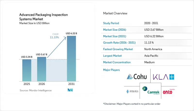
에 의하면, 첨단 패키징 검사 시스템 시장 규모는 2025년에 33억 4,000만 달러, 2026년에 36억 7,000만 달러로 추정되고, 2031년까지 62억 2,000만 달러에 이를 것으로 예측되며, 2026-2031년 CAGR 11.13%를 기록할 전망입니다.
세계 첨단 패키징 검사 시스템 시장 동향 및 인사이트
AI와 고성능 컴퓨팅이 이종 통합을 주도
AI 가속기 패키지는 여러 개의 다이, 고밀도 상호 연결 구조, 그리고 서로 다른 공정 이력을 가진 재료가 결합되어 있어 검사가 가장 어려운 디바이스 중 하나입니다. 모든 패키징 웨이퍼는 고부가가치 시스템을 지원하기 전에 입고 기판의 품질, 구리 재배선 층의 패터닝, 마이크로 범프의 평탄도, 다이의 배치 및 최종 패키지의 무결성에 대한 검사를 받아야 합니다. KLA는 자사의 반도체 공정 제어 포트폴리오에서 첨단 패키징 매출이 2025년 6억 3,500만 달러에서 2026년에는 10억 달러로 증가할 것으로 전망한다고 밝혔습니다. 이 회사의 이러한 전망은 공정 제어에 대한 지출을 패키징 역량 강화 및 이종 패키지에 사용되는 측정 단계 수 증가와 연계하고 있습니다. 생산 능력 확대에 따라 최종 검사에만 의존하지 않고 제조의 여러 단계에서 검사가 필요해질 경우, 첨단 패키징 검사 시스템 시장은 혜택을 볼 것입니다. 또한, 고가의 멀티다이 패키지의 경우 완제품 1개당 검사 범위가 넓어지기 때문에 첨단 패키징 검사 시스템 시장의 장비 수요는 칩 출하량에 대한 의존도도 낮아집니다.
하이브리드 본딩 및 파인 피치 상호 연결의 채택 확대
하이브리드 본딩에는 극히 미세한 구조, 매립 계면, 표면 상태 및 생산 처리량을 동시에 처리할 수 있는 검사 기법이 요구됩니다. ASM 전자 소자 고장 분석 협회의 조사에 따르면, 모든 하이브리드 본딩 공정에서 나노 스케일의 해상도, 전체 영역의 커버리지, 표면 아래의 가시성, 그리고 제조 공정에 적합한 처리량을 동시에 충족하는 단일 기법은 존재하지 않는 것으로 밝혀졌습니다. 따라서 첨단 패키징 검사 시스템 시장의 각 제조업체는 하이브리드 본딩 검사를 단일 장비 구매로 취급하지 않고, 본딩 공정의 각 단계에서 광학, 적외선, 음향, X선과 같은 서로 다른 접근 방식을 채택하고 있습니다. Onto Innovation사는 입자 높이를 측정하는 3D 계측 기술과 유전체 층 내의 보이드를 식별할 수 있는 적외선 검사를 결합한 인라인형 하이브리드 본딩 툴에 대해 설명했습니다. Nova사는 2026년 7월, 세계 유수의 주조 기업이 경쟁사 평가를 거쳐 자사의 WMC 플랫폼을 첨단 패키징 측정의 표준 장비로 선정했다고 발표했습니다. 하이브리드 본딩을 통해 단일 검사 지점이 여러 물리적 측정 요건을 수반하는 광범위한 공정 제어 시퀀싱로 변화함에 따라, 이러한 움직임은 첨단 패키징 검사 시스템 시장의 확대로 이어질 것입니다.
높은 설비 투자 및 총 소유 비용
생산 라인에서 여러 검사 기술을 사용하는 경우, 첨단 패키징 검사 시스템에는 막대한 설비 투자가 필요합니다. 또한, 장비는 클린룸 운영 및 유지보수 체계와도 통합되어야 합니다. 하이브리드 본딩 라인에서는 광학, 적외선, 음향, X선 등의 장비가 필요할 수 있으며, 각 시스템은 서로 다른 물리적 측정 요건을 충족합니다. 이러한 비용 부담은 장비 예산이 제한적이고 인라인 검사를 전면적으로 커버할 재정적 여유가 부족한 반도체 조립 및 테스트 수탁 업체에게 특히 큰 과제가 되고 있습니다. Onto Innovation사는 2026년 3월, 단일 플랫폼에서 여러 HBM4 관련 용도를 지원할 수 있도록 설계된 광학 시스템 및 조명 시스템을 탑재한 ‘Dragonfly G5’를 출시했습니다. 이 플랫폼의 설계는 첨단 패키징 워크플로우에 필요한 감도를 유지하면서도, 용도별로 개별 장비를 추가하지 않고도 더 폭넓은 기능을 원하는 고객의 요구를 반영한 것입니다. 첨단 패키징 검사 시스템 시장의 소규모 진출기업들은 종합적인 인라인 검사 도입에 필요한 자금을 조달하기 어려운 경우, 샘플링 검사를 계속 채택할 가능성이 있습니다. 다만, 샘플링 검사의 경우 복잡한 멀티다이 제품에서 수율 위험이 높아질 수 있습니다.
부문 분석
2025년, 광학식 검사·계측 시스템은 첨단 패키징 검사 시스템 시장 점유율의 42.51%를 차지했습니다. 이러한 선도적 지위는 높은 처리량, 웨이퍼 레벨 및 조립 후 공정에서의 폭넓은 활용, 그리고 웨이퍼 팹 및 외부 위탁 조립 거점에서의 확고한 도입 실적을 반영합니다. 이러한 시스템은 여러 패키지 유형에 걸친 재배선 층의 크리티컬 디멘션 측정, 범프의 평탄도 검사, 다이 시프트 감지 및 매크로 결함 스크리닝을 지원합니다. 팬아웃 및 플립칩 생산에서 이러한 시스템의 활용은 대량 생산 공정에서 검사 속도와 비용을 관리해야 할 필요성과 부합합니다. Onto Innovation은 2026년 3월, 첨단 패키징 용도를 위해 150nm의 결함 감도와 멀티모드 조명을 갖춘 ‘Dragonfly G5’를 출시했습니다.
적외선 및 열화상 시스템은 적층 다이 구조 내의 표면 아래 보이드나 박리를 감지하는 반면, 음향 시스템은 표면 광학 기법으로는 감지할 수 없는 언더필이나 봉지재의 문제를 파악합니다. 전자빔 검사는 실리콘 관통 비아(TSV) 및 백엔드 상호 연결에 대한 전기적 콘트라스트 이미지를 제공하며, SPIE의 논문에서는 AI를 통한 계산 샘플링을 통해 결함 다이 감지율이 최대 4.3배 향상되었다고 보고되었습니다. X선 및 컴퓨터 단층 촬영(CT) 검사 시스템은 2031년까지 연평균 성장률(CAGR) 14.80%를 나타낼 것으로 예측되며, 이 부문에서 가장 높은 성장률을 보이고 있습니다. 『Research in Microelectronics Reliability』 저널에 따르면, 고해상도 나노 CT는 30초간의 개요 스캔 동안 20µm 크기의 마이크로 범프 내 서브미크론 크기의 공극이나 균열을 감지했습니다. 이 기능을 통해 광학 시스템으로는 직접 평가할 수 없는 매립 접합부, HBM의 전도성, 그리고 하이브리드 본딩 계면의 검사가 가능해집니다.
2025년 기준, 조립 후 검사는 첨단 패키징 검사 시스템 분야에서 34.26%의 점유율을 차지했습니다. 이 점유율은 다이싱 후 및 패키지 조립 공정에서 사용되는 자동 광학 검사(AOI) 및 3D 검사 시스템의 도입 실적을 반영합니다. 이러한 도구는 출하 전에 패키지의 외관, 솔더 관련 특성, 정렬 및 기타 육안으로 확인 가능한 상태를 평가합니다. 이 범주는 성숙한 패키징 기법으로 제조된 디바이스를 포함하여 모든 패키지에 여전히 필수적입니다. 또한, 여러 고객 프로그램에 걸쳐 대량 생산을 수행하는 외부 위탁 조립 업무에도 활용되고 있습니다.
첨단 패키징 검사 시스템 시장에서 웨이퍼 레벨 검사는 2031년까지 연평균 성장률(CAGR) 14.29%로 확대될 것으로 예측됩니다. 이는 다이 부착 전에 결함을 발견함으로써 완성된 멀티 다이 패키지의 손실을 방지할 수 있기 때문입니다. 2025년 12월 『Journal of Manufacturing Science and Engineering』지에 게재된 리뷰에 따르면, 실리콘 관통 비아(TSV), 하이브리드 본딩 계면 및 마이크로 범프 어레이로 인해 표면 및 표면 하부 검사에 대한 요구 사항이 높아지고 있는 것으로 밝혀졌습니다. Nova사는 2025년 8월, 2.5D 및 3D 통합, 하이브리드 본딩, 그리고 다양한 웨이퍼 크기를 지원하는 모듈형 광학 계측 플랫폼으로 WMC를 출시했습니다. 다이 레벨 검사를 통해 알려진 결함이 있는 다이가 멀티 다이 어셈블리에 혼입되는 것을 방지하는 한편, 최종 검사 및 고장 분석을 통해 그 결과가 업스트림 공정 팀에 피드백됩니다. Cohu사는 자사의 Neon 플랫폼이 2026년 대만의 외부 위탁 조립 거점에서 HBM3, HBM4 및 HBM4E 용도를 위한 인증 테스트를 받고 있다고 밝혔습니다.
지역별 분석
2025년, 아시아태평양은 첨단 패키징 검사 시스템 분야에서 59.81%의 점유율을 차지했습니다. 이러한 위상은 해당 지역에 첨단 패키징 역량, 메모리 생산 및 반도체 수탁 조립 사업이 집중되어 있기 때문입니다. 『타이베이 타임스』가 보도한 ITRI의 데이터에 따르면, 2024년 세계 IC 패키징 및 테스트 생산량의 50% 가까이를 대만이 차지하고 있으며, 한국도 주요 HBM 패키징 활동을 수행하고 있습니다. 일본은 정밀 광학 기기, 전자빔 장비 공급업체, 반도체 조립 수탁 생산 및 메모리 패키징 생산 능력을 제공합니다. 이러한 생산 거점의 존재로 인해 이 지역은 신규 설비 도입 및 현장 서비스 분야에서 중요한 위치를 차지하고 있습니다.
중국은 첨단 패키징 검사 시스템 시장에서 대규모의 기존 패키징 기반을 보유하고 있으며, 국산 검사 장비에 대한 관심이 높아지고 있습니다. 캠텍(Camtech)의 보고서에 따르면, 2026년 해당 기업의 매출의 45%를 중국이 차지할 것으로 전망됩니다. 대만 이외 지역의 수탁 조립 생산 능력이 확대됨에 따라 말레이시아, 베트남, 싱가포르의 중요성이 커지고 있습니다. 이들 국가의 생산 능력은 기존 시설의 리드타임이 길어질 경우 수요의 일부를 흡수할 수 있습니다.
첨단 패키징 검사 시스템 시장에서 북미는 2031년까지 연평균 성장률(CAGR) 14.50%를 나타낼 것으로 예측되며, 가장 빠르게 성장하는 지역이 될 전망입니다. SK하이닉스는 2026년 8월 인디애나주에서 HBM 패키징 시설의 기공식을 가졌으며, 이 시설은 2030년까지 북미의 HBM 생산 거점이 될 것으로 기대됩니다. 미국의 공공 보조금은 패키징 연구, 시범 생산 능력, 기판 개발 및 소재 연구를 지원하고 있습니다. 캐나다는 패키징 연구를 지원하고 있으며, 멕시코는 백엔드 조립 및 테스트 분야에서 역할을 수행하고 있습니다. 유럽은 비교적 소극적인 입장을 취하고 있으며, X선, X선 형광, 원자력 현미경 측정 분야에 대응하는 독일과 네덜란드공급업체들이 주도하고 있습니다. 남미, 중동 및 아프리카는 여전히 소규모 시장이며, 수요는 수탁 조립 및 테스트에 대한 투자와 연동되어 있습니다.
기타 혜택:
- 엑셀 형식 시장 예측(ME) 시트
- 3개월간의 애널리스트 지원
목차
제1장 서론
- 조사의 전제조건과 시장의 정의
- 조사 범위
제2장 조사 방법
제3장 주요 요약
제4장 시장 구도
- 시장 개요
- 시장 성장 촉진요인
- 시장 성장 억제요인
- 거시경제 요인이 시장에 미치는 영향
- 업계 밸류체인 분석
- 규제 상황
- 기술 전망
- Porter의 Five Forces 분석
제5장 시장 규모와 성장 예측
- 검사 기술별
- 검사 단계별
- 패키징 플랫폼별
- 최종사용자 산업별
- 지역별
- 북미
- 미국
- 캐나다
- 멕시코
- 남미
- 브라질
- 아르헨티나
- 기타 남미 국가
- 유럽
- 독일
- 영국
- 프랑스
- 이탈리아
- 스페인
- 기타 유럽 국가
- 아시아태평양
- 중국
- 일본
- 인도
- 한국
- ASEAN
- 기타 아시아태평양 국가
- 중동 및 아프리카
- 중동
- 사우디아라비아
- 아랍에미리트(UAE)
- 튀르키예
- 기타 중동 국가
- 아프리카
- 남아프리카공화국
- 나이지리아
- 기타 아프리카 국가
- 중동
- 북미
제6장 경쟁 구도
- 시장 집중도
- 전략적 동향
- 시장 점유율 분석
- 기업 개요
- KLA Corporation
- Onto Innovation Inc.
- Camtek Ltd.
- Cohu, Inc.
- Intekplus Co., Ltd.
- Semiconductor Technologies and Instruments Pte. Ltd.
- Lasertec Corporation
- Unity Semiconductor SAS
- Shenzhen Skyverse Technology Co., Ltd.
- Cheng Mei Instrument Technology Co., Ltd.
- Chroma ATE Inc.
- Toray Engineering Co., Ltd.
- TASMIT, Inc.
- Confovis GmbH
- Nova Ltd.
- Bruker Corporation
- Nearfield Instruments B.V.
- Comet Yxlon GmbH
- Hitachi High-Tech Corporation
- Tokyo Electron Limited
- JEOL Ltd.
제7장 시장 기회와 향후 전망
LSHAccording to Mordor Intelligence, the advanced packaging inspection systems market size was USD 3.34 billion in 2025, and USD 3.67 billion in 2026, and is projected to reach USD 6.22 billion by 2031, growing at a CAGR of 11.13% during 2026-2031.
Global Advanced Packaging Inspection Systems Market Trends and Insights
AI and High-Performance Computing Driving Heterogeneous Integration
AI accelerator packages are among the most difficult devices to inspect because they combine several dies, dense interconnect structures, and materials with different process histories. Every packaging wafer requires checks of incoming substrate quality, copper redistribution layer patterning, micro-bump coplanarity, die placement, and final package integrity before it can support a high-value system. KLA stated that advanced packaging revenue in its semiconductor process control portfolio was expected to rise from USD 635 million in 2025 to USD 1 billion in 2026. This company result links process-control spending to added packaging capacity and to the larger number of measurement steps used on heterogeneous packages. The advanced packaging inspection systems market benefits when capacity additions require inspection at multiple manufacturing stages rather than relying on a final check alone. Tool demand in the advanced packaging inspection systems market also becomes less dependent on chip volumes because costly multi-die packages require greater inspection coverage for each finished unit.
Rising Hybrid Bonding and Fine-Pitch Interconnect Adoption
Hybrid bonding requires inspection methods that can address very small features, buried interfaces, surface conditions, and production throughput at the same time. An ASM Electronic Device Failure Analysis Society study found that no single method provides nanoscale resolution, full-field coverage, subsurface visibility, and manufacturing-compatible throughput across all hybrid-bonding stages. Manufacturers in the advanced packaging inspection systems market, therefore, use optical, infrared, acoustic, and X-ray approaches at distinct points in the bonding flow, rather than treating hybrid-bond inspection as one tool purchase. Onto Innovation described in-line hybrid-bonding tools that combine 3D metrology for particle-height measurement with infrared inspection that can identify voids in dielectric layers. Nova announced in July 2026 that a leading global foundry had selected its WMC platform as its tool of record for advanced packaging measurements following a competitive evaluation. This shift expands the advanced packaging inspection systems market because hybrid bonding transforms a single inspection point into a broader process-control sequence with multiple physical measurement requirements.
High Capital and Total Cost of Ownership
Advanced packaging inspection systems require significant capital outlay when a production line uses several inspection technologies, and the equipment must also be integrated with cleanroom operations and maintenance practices. A hybrid-bonding line may need optical, infrared, acoustic, and X-ray tools, with each system serving a different physical measurement requirement. That cost burden is especially difficult for outsourced semiconductor assembly and test providers with narrower equipment budgets and less room to fund full inline coverage. Onto Innovation launched Dragonfly G5 in March 2026 with an optics and illumination design intended to support several HBM4-related applications on one platform. The platform's design reflects customer demand for broader capability without adding a separate tool for every application, while preserving the sensitivity needed for advanced package workflows. Smaller participants in the advanced packaging inspection systems market may continue to use sampling where comprehensive inline inspection is difficult to fund, even though sampling can leave more yield risk in complex multi-die products.
Other drivers and restraints analyzed in the detailed report include:
- Expansion of HBM and 3D Memory Stacking
- Government Incentives for Domestic Advanced Packaging Capacity
- Shortage of Advanced Packaging Metrology Talent
For complete list of drivers and restraints, kindly check the Table Of Contents.
Segment Analysis
Optical-based inspection and metrology systems held 42.51% of the advanced packaging inspection systems market share in 2025. Their leading position reflects high throughput, broad use across wafer-level and post-assembly flows, and an established installed base at wafer fabs and outsourced assembly sites. These systems support redistribution layer critical-dimension measurement, bump coplanarity checks, die-shift detection, and macro-defect screening across several package types. Their use in fan-out and flip-chip production aligns with the need to manage inspection speed and cost in high-volume flows. Onto Innovation launched Dragonfly G5 in March 2026 with stated 150 nm defect sensitivity and multi-mode illumination for advanced packaging applications.
Infrared and thermal systems find subsurface voids and delamination in stacked-die structures, while acoustic systems identify underfill and encapsulant issues beyond the reach of surface optical methods. Electron-beam inspection provides electrical-contrast imaging for through-silicon vias and back-end interconnects, and an SPIE paper reported defective-die capture rates up to 4.3 times higher through AI-guided computational sampling. X-ray and computed tomography inspection systems are projected to grow at a 14.80% CAGR through 2031, the highest rate in this segmentation. Research in Microelectronics Reliability showed that high-resolution nano-CT detected sub-micron voids and cracks in 20 µm micro-bumps during a 30-second overview scan. This capability supports inspection of buried joints, HBM continuity, and hybrid-bond interfaces that optical systems cannot directly assess.
Post-assembly inspection held 34.26% of the share in the advanced packaging inspection systems sector in 2025. Its position reflects the installed base of automated optical inspection and 3D inspection systems used after dicing and during package assembly. These tools assess package appearance, solder-related features, alignment, and other visible conditions before shipment. The category remains necessary for every package, including devices made through mature packaging methods. It also serves outsourced assembly operations that process high volumes across multiple customer programs.
Wafer-level inspection in the advanced packaging inspection systems market is projected to expand at a 14.29% CAGR through 2031 because defects found before die attach can prevent loss in a completed multi-die package. A December 2025 review in the Journal of Manufacturing Science and Engineering found that through-silicon vias, hybrid bonding interfaces, and micro-bump arrays are raising requirements for surface and subsurface inspection. Nova released the WMC in August 2025 as a modular optical metrology platform for 2.5D and 3D integration, hybrid bonding, and different wafer sizes. Die-level inspection prevents known-defective dies from entering multi-die assemblies, while final inspection and failure analysis feed findings back to upstream process teams. Cohu stated that its Neon platform was being qualified at a Taiwan-based outsourced assembly site for HBM3, HBM4, and HBM4E applications in 2026.
Complete Report Scope:
- By Inspection Technology
- Optical-Based Inspection and Metrology Systems
- Infrared and Thermal Inspection Systems
- X-Ray and Computed Tomography Inspection Systems
- Electron-Beam Inspection Systems
- Acoustic and Other Inspection Systems
- By Inspection Stage
- Wafer-Level Inspection
- Die-Level and Component Inspection
- Post-Assembly Inspection
- Final Inspection and Failure Analysis
- By Packaging Platform
- 2.5D Interposer Packaging
- 3D Integrated Circuit and HBM Packaging
- Fan-Out Packaging
- Fan-In Packaging
- Panel-Level Packaging
- System-in-Package
- Hybrid-Bonded Packaging
- Embedded-Die and Chiplet Packaging
- By End-User Industries
- Consumer Electronics
- Data Centers and High-Performance Computing
- Automotive and Electric Vehicles
- Telecommunications and Networking
- Healthcare and Medical Devices
- Aerospace and Defense
- Research and Academic Institutions
- Other End-User Industries
- By Geography
- North America
- United States
- Canada
- Mexico
- South America
- Brazil
- Argentina
- Rest of South America
- Europe
- Germany
- United Kingdom
- France
- Italy
- Spain
- Rest of Europe
- Asia-Pacific
- China
- Japan
- India
- South Korea
- ASEAN
- Rest of Asia-Pacific
- Middle East and Africa
- Middle East
- Saudi Arabia
- United Arab Emirates
- Turkey
- Rest of the Middle East
- Africa
- South Africa
- Nigeria
- Rest of Africa
- Middle East
- North America
Geography Analysis
Asia-Pacific held 59.81% of the share in the advanced packaging inspection systems sector in 2025. Its position follows the region's concentration of advanced packaging capacity, memory production, and outsourced semiconductor assembly operations. Taiwan accounted for nearly 50% of global IC packaging and testing output in 2024, based on ITRI data reported by the Taipei Times, and South Korea adds major HBM packaging activity. Japan contributes precision optics, electron-beam suppliers, outsourced assembly operations, and memory packaging capacity. These production centers make the region important for new equipment installations and field service.
China has a large legacy packaging base within the advanced packaging inspection systems market and an increasing interest in domestically sourced inspection equipment. Camtek reported that China represented 45% of its 2026 revenue. Malaysia, Vietnam, and Singapore are gaining relevance as outsourced assembly capacity expands beyond Taiwan. Their capacity can absorb part of the demand when lead times at established facilities lengthen.
North America in the advanced packaging inspection systems market is projected to grow at a 14.50% CAGR through 2031, making it the fastest-growing geography. SK Hynix held a groundbreaking ceremony in August 2026 for an HBM packaging facility in Indiana that was expected to be a North American HBM production base by 2030. U.S. public awards support packaging research, pilot capacity, substrate development, and materials work. Canada supports packaging research, and Mexico has a role in back-end assembly and test. Europe has a more modest position, led by German and Dutch suppliers serving X-ray, X-ray fluorescence, and atomic-force-metrology applications. South America and the Middle East and Africa remain smaller markets where demand follows contract assembly and test investment.
- KLA Corporation
- Onto Innovation Inc.
- Camtek Ltd.
- Cohu, Inc.
- Intekplus Co., Ltd.
- Semiconductor Technologies and Instruments Pte. Ltd.
- Lasertec Corporation
- Unity Semiconductor SAS
- Shenzhen Skyverse Technology Co., Ltd.
- Cheng Mei Instrument Technology Co., Ltd.
- Chroma ATE Inc.
- Toray Engineering Co., Ltd.
- TASMIT, Inc.
- Confovis GmbH
- Nova Ltd.
- Bruker Corporation
- Nearfield Instruments B.V.
- Comet Yxlon GmbH
- Hitachi High-Tech Corporation
- Tokyo Electron Limited
- JEOL Ltd.
Additional Benefits:
- The market estimate (ME) sheet in Excel format
- 3 months of analyst support
TABLE OF CONTENTS
1 INTRODUCTION
- 1.1 Study Assumptions and Market Definition
- 1.2 Scope of the Study
2 RESEARCH METHODOLOGY
3 EXECUTIVE SUMMARY
4 MARKET LANDSCAPE
- 4.1 Market Overview
- 4.2 Market Drivers
- 4.2.1 AI and High-Performance Computing Driving Heterogeneous Integration
- 4.2.2 Rising Hybrid Bonding and Fine-Pitch Interconnect Adoption
- 4.2.3 Expansion of HBM and 3D Memory Stacking
- 4.2.4 Government Incentives for Domestic Advanced Packaging Capacity
- 4.2.5 Growth of Panel-Level Packaging and Glass-Core Substrates
- 4.2.6 Increasing Yield Economics of Inline Multimodal Inspection
- 4.3 Market Restraints
- 4.3.1 High Capital and Total Cost of Ownership
- 4.3.2 Shortage of Advanced Packaging Metrology Talent
- 4.3.3 Specialty Component and Supply-Chain Constraints
- 4.3.4 Data-Integration and Cybersecurity Risk in Connected Inspection
- 4.4 Impact of Macroeconomic Factors on the Market
- 4.5 Industry Value-Chain Analysis
- 4.6 Regulatory Landscape
- 4.7 Technological Outlook
- 4.7.1 Optical and Multispectral Inspection
- 4.7.2 Infrared and Subsurface Inspection
- 4.7.3 2D, 3D, and X-Ray Computed Tomography
- 4.7.4 AI-Based Defect Classification and Predictive Process Control
- 4.7.5 Hybrid Bonding and Chiplet Inspection
- 4.7.6 In-Situ and Inline Inspection
- 4.7.7 Panel-Level and Glass-Substrate Inspection
- 4.8 Porter's Five Forces Analysis
- 4.8.1 Bargaining Power of Suppliers
- 4.8.2 Bargaining Power of Buyers
- 4.8.3 Threat of New Entrants
- 4.8.4 Threat of Substitutes
- 4.8.5 Intensity of Competitive Rivalry
5 MARKET SIZE AND GROWTH FORECASTS (VALUE)
- 5.1 By Inspection Technology
- 5.1.1 Optical-Based Inspection and Metrology Systems
- 5.1.2 Infrared and Thermal Inspection Systems
- 5.1.3 X-Ray and Computed Tomography Inspection Systems
- 5.1.4 Electron-Beam Inspection Systems
- 5.1.5 Acoustic and Other Inspection Systems
- 5.2 By Inspection Stage
- 5.2.1 Wafer-Level Inspection
- 5.2.2 Die-Level and Component Inspection
- 5.2.3 Post-Assembly Inspection
- 5.2.4 Final Inspection and Failure Analysis
- 5.3 By Packaging Platform
- 5.3.1 2.5D Interposer Packaging
- 5.3.2 3D Integrated Circuit and HBM Packaging
- 5.3.3 Fan-Out Packaging
- 5.3.4 Fan-In Packaging
- 5.3.5 Panel-Level Packaging
- 5.3.6 System-in-Package
- 5.3.7 Hybrid-Bonded Packaging
- 5.3.8 Embedded-Die and Chiplet Packaging
- 5.4 By End-User Industries
- 5.4.1 Consumer Electronics
- 5.4.2 Data Centers and High-Performance Computing
- 5.4.3 Automotive and Electric Vehicles
- 5.4.4 Telecommunications and Networking
- 5.4.5 Healthcare and Medical Devices
- 5.4.6 Aerospace and Defense
- 5.4.7 Research and Academic Institutions
- 5.4.8 Other End-User Industries
- 5.5 By Geography
- 5.5.1 North America
- 5.5.1.1 United States
- 5.5.1.2 Canada
- 5.5.1.3 Mexico
- 5.5.2 South America
- 5.5.2.1 Brazil
- 5.5.2.2 Argentina
- 5.5.2.3 Rest of South America
- 5.5.3 Europe
- 5.5.3.1 Germany
- 5.5.3.2 United Kingdom
- 5.5.3.3 France
- 5.5.3.4 Italy
- 5.5.3.5 Spain
- 5.5.3.6 Rest of Europe
- 5.5.4 Asia-Pacific
- 5.5.4.1 China
- 5.5.4.2 Japan
- 5.5.4.3 India
- 5.5.4.4 South Korea
- 5.5.4.5 ASEAN
- 5.5.4.6 Rest of Asia-Pacific
- 5.5.5 Middle East and Africa
- 5.5.5.1 Middle East
- 5.5.5.1.1 Saudi Arabia
- 5.5.5.1.2 United Arab Emirates
- 5.5.5.1.3 Turkey
- 5.5.5.1.4 Rest of the Middle East
- 5.5.5.2 Africa
- 5.5.5.2.1 South Africa
- 5.5.5.2.2 Nigeria
- 5.5.5.2.3 Rest of Africa
- 5.5.5.1 Middle East
- 5.5.1 North America
6 COMPETITIVE LANDSCAPE
- 6.1 Market Concentration
- 6.2 Strategic Moves
- 6.3 Market Share Analysis
- 6.4 Company Profiles (includes Global Level Overview, Market Level Overview, Core Segments, Financials as available, Strategic Information, Market Rank/Share, Products and Services, Recent Developments)
- 6.4.1 KLA Corporation
- 6.4.2 Onto Innovation Inc.
- 6.4.3 Camtek Ltd.
- 6.4.4 Cohu, Inc.
- 6.4.5 Intekplus Co., Ltd.
- 6.4.6 Semiconductor Technologies and Instruments Pte. Ltd.
- 6.4.7 Lasertec Corporation
- 6.4.8 Unity Semiconductor SAS
- 6.4.9 Shenzhen Skyverse Technology Co., Ltd.
- 6.4.10 Cheng Mei Instrument Technology Co., Ltd.
- 6.4.11 Chroma ATE Inc.
- 6.4.12 Toray Engineering Co., Ltd.
- 6.4.13 TASMIT, Inc.
- 6.4.14 Confovis GmbH
- 6.4.15 Nova Ltd.
- 6.4.16 Bruker Corporation
- 6.4.17 Nearfield Instruments B.V.
- 6.4.18 Comet Yxlon GmbH
- 6.4.19 Hitachi High-Tech Corporation
- 6.4.20 Tokyo Electron Limited
- 6.4.21 JEOL Ltd.
7 MARKET OPPORTUNITIES AND FUTURE OUTLOOK
- 7.1 White-Space and Unmet-Need Assessment


