


|
시장보고서
상품코드
1959278
3D 칩 스태킹 기술 시장 기회, 성장요인, 업계 동향 분석 및 예측(2026-2035년)3D Chip Stacking Market Opportunity, Growth Drivers, Industry Trend Analysis, and Forecast 2026 - 2035 |
||||||
세계의 3D 칩 스태킹 시장은 2025년에 8억 870만 달러로 평가되었고, 2035년까지 연평균 복합 성장률(CAGR) 20.7%로 성장하여 52억 5,000만 달러에 이를 것으로 예측됩니다.

시장 확대는 이기종 통합에 대한 수요 증가, 고급 프로세스 노드의 비용 최적화, AI 및 고성능 컴퓨팅 워크로드 확대, 설계 유연성 향상, 개방형 인터커넥트를 통한 에코시스템 표준화에 의해 주도되고 있습니다. 3D 칩 스태킹 기술은 여러 개의 집적회로 다이를 단일 패키지 내에서 수직 적층 및 상호 연결이 가능한 현대 반도체 혁신의 기반 기술이 되었습니다. 이를 통해 상호 연결 거리 단축, 신호 전송 속도 향상, 전력 효율 향상, 소형 실적 내 높은 트랜지스터 밀도 구현이 가능합니다. 각국 정부는 국내 반도체 역량과 공급망 회복력을 강화하기 위한 산업 정책의 일환으로 첨단 패키징을 적극 지원하고 있습니다. 이 기술은 저전력 소비와 컴팩트한 디자인을 유지하면서 높은 연산 성능을 필요로 하는 AI 가속기, IoT 디바이스, HPC 플랫폼, 차세대 전자제품에서 점점 더 중요성이 커지고 있습니다. 반도체 생태계가 성숙해짐에 따라 3D 적층 기술은 미래 전자제품의 확장성과 성능을 구현하는 중요한 기반 기술이 될 것입니다.
| 시장 범위 | |
|---|---|
| 개시 연도 | 2025년 |
| 예측 연도 | 2026-2035년 |
| 개시 연도 가치 | 8억 870만 달러 |
| 예측 금액 | 52억 5,000만 달러 |
| CAGR | 20.7% |
2.5D 통합 부문은 2025년 2억 8,530만 달러에 달했습니다. 2.5D 아키텍처는 인터포저에 여러 개의 다이를 병렬로 배치하여 AI, HPC, 네트워킹, 그래픽 집약적 용도에 필수적인 고대역폭, 저지연, 고밀도 인터커넥션을 구현합니다. 정부 지원 프로그램 및 R&D 이니셔티브는 인터포저 개발을 가속화하고 데이터센터 및 통신 인프라를 위한 에너지 절약 솔루션을 제공함으로써 2.5D 집적 기술의 채택을 촉진하고 있습니다. 제조업체들은 고 대역폭, 저 지연 요구사항에 대응하기 위해 인터포저 기반 2.5D 솔루션에 대한 투자를 장려하는 한편, 정책적 지원을 통해 차세대 반도체 용도의 발전을 도모하고 있습니다.
실리콘 관통 전극(TSV) 부문은 2025년 2억 7,720만 달러 시장 규모를 형성할 것으로 예측됩니다. TSV 기술은 적층 다이 간 수직 상호 연결을 가능하게 하고, 신호 지연 감소, 전력 효율 향상, 열 관리 지원을 위해 AI 가속기, HPC 시스템, 데이터센터용 메모리 스택에 필수적인 기술입니다. 칩 밀도와 성능을 최적화하면서 에너지 소비와 설치 공간을 최소화하는 기업 및 정부의 우선순위에 따라 TSV의 채택이 가속화되고 있습니다. TSV를 활용한 고성능 메모리 및 로직 스택에 집중하는 제조업체는 정부 주도의 R&D 인센티브의 혜택을 누리면서 AI 및 데이터 집약적 용도 증가하는 컴퓨팅 수요에 대응할 수 있는 유리한 입지를 확보할 수 있습니다.
북미 3D 칩 스태킹 시장은 2025년 27.3%의 점유율을 차지했습니다. 이 지역의 급속한 성장은 성숙한 기술 생태계, 강력한 R&D 인프라, AI, 자동차, 데이터센터용도 수요 증가에 힘입은 바 큽니다. 인텔, 엔비디아, AMD 등 주요 반도체 기업들은 이기종 통합 및 고밀도 패키징의 기술 혁신을 추진하고 있습니다. 첨단 패키징 및 3D 적층기술에 대한 자금 지원 프로그램 등 정부 시책은 국내 제조 역량 강화와 해외 생산 의존도를 낮추는데 기여하고 있습니다. 북미 기업들은 고성능 컴퓨팅, AI, 국방 시장의 기회를 잡기 위해 연방 정부 프로그램에 따라 3D 적층 생산 라인을 확장하고 있습니다.
자주 묻는 질문
목차
제1장 조사 방법과 범위
제2장 주요 요약
제3장 업계 인사이트
제4장 경쟁 구도
제5장 시장 추산 및 예측 : 적층 구조별, 2022-2035
제6장 시장 추산 및 예측 : 컴포넌트별, 2022-2035
제7장 시장 추산 및 예측 : 기술별, 2022-2035
제8장 시장 추산 및 예측 : 폼팩터별, 2022-2035
제9장 시장 추산 및 예측 : 용도별, 2022-2035
제10장 시장 추산 및 예측 : 최종 이용 산업별, 2022-2035
제11장 시장 추산 및 예측 : 지역별, 2022-2035
제12장 기업 개요
LSH 26.03.18The Global 3D Chip Stacking Market was valued at USD 808.7 million in 2025 and is estimated to grow at a CAGR of 20.7% to reach USD 5.25 billion by 2035.
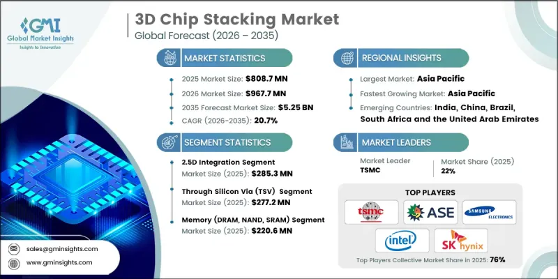
The market's expansion is fueled by rising demand for heterogeneous integration, cost optimization at advanced process nodes, AI and high-performance computing workload scaling, improved design flexibility, and ecosystem standardization through open interconnects. 3D chip stacking has become a cornerstone of modern semiconductor innovation, allowing multiple integrated circuit dies to be vertically stacked and interconnected within a single package. This approach reduces interconnect distances, accelerates signal transmission, enhances power efficiency, and enables a higher transistor density within compact footprints. Governments worldwide are actively supporting advanced packaging as part of industrial policies to strengthen domestic semiconductor capabilities and supply chain resilience. Technology is increasingly critical for AI accelerators, IoT devices, HPC platforms, and next-generation electronics that require high computational performance while maintaining low energy consumption and compact designs. As semiconductor ecosystems mature, 3D stacking is poised to be a key enabler of future electronics scalability and performance.
| Market Scope | |
|---|---|
| Start Year | 2025 |
| Forecast Year | 2026-2035 |
| Start Value | $808.7 Million |
| Forecast Value | $5.25 Billion |
| CAGR | 20.7% |
The 2.5D integration segment reached USD 285.3 million in 2025. 2.5D architectures place multiple dies side-by-side on an interposer, delivering high bandwidth, reduced latency, and enhanced interconnect density, which are essential for AI, HPC, networking, and graphics-intensive applications. The adoption of 2.5D integration is being reinforced by government-backed programs and R&D initiatives that accelerate interposer development and provide energy-efficient solutions for data centers and telecommunications infrastructure. Manufacturers are encouraged to invest in interposer-based 2.5D solutions to address high-bandwidth and low-latency requirements while leveraging policy support to advance next-generation semiconductor applications.
The through silicon via (TSV) segment generated USD 277.2 million in 2025. TSV technology enables vertical interconnects across stacked dies, reducing signal delay, improving power efficiency, and supporting thermal management, making it indispensable for AI accelerators, HPC systems, and data center memory stacks. Adoption of TSV is being reinforced by enterprise and government priorities to optimize chip density and performance while minimizing energy consumption and footprint. Manufacturers focusing on TSV-enabled high-performance memory and logic stacks are well-positioned to meet the increasing computational demands of AI and data-intensive applications while benefiting from government-sponsored R&D incentives.
North America 3D Chip Stacking Market accounted for 27.3% share in 2025. The region's rapid growth is supported by a mature technology ecosystem, strong R&D infrastructure, and rising demand from AI, automotive, and data center applications. Leading semiconductor companies, including Intel, NVIDIA, and AMD, are driving innovation in heterogeneous integration and high-density packaging. Government initiatives, such as funding programs for advanced packaging and 3D stacking, are enhancing domestic manufacturing capabilities and reducing dependence on overseas production. Companies in North America are scaling 3D stacking production lines in alignment with federal programs to capture high-performance computing, AI, and defense market opportunities.
Key players operating in the Global 3D Chip Stacking Market include TSMC, Intel Corporation, Samsung Electronics, Micron Technology, SK hynix, NVIDIA, Broadcom, Qualcomm, ASE Technology Holding, Amkor Technology, JCET Group, Powertech Technology Inc. (PTI), Sony Semiconductor Solutions, Toshiba (Kioxia Holdings), and Texas Instruments. Companies in the Global 3D Chip Stacking Market are strengthening their foothold by investing heavily in R&D for heterogeneous integration, high-density interposers, and TSV-enabled designs. Many firms are forming strategic alliances with foundries, memory suppliers, and AI platform developers to co-develop optimized chip architectures. Vertical integration strategies are being employed to enhance supply chain control and reduce production risks. Manufacturers are also focusing on government-backed initiatives to expand domestic manufacturing, improve thermal management solutions, and scale advanced packaging lines.
Table of Contents
Chapter 1 Methodology and Scope
- 1.1 Market scope and definition
- 1.2 Research design
- 1.2.1 Research approach
- 1.2.2 Data collection methods
- 1.3 Data mining sources
- 1.3.1 Global
- 1.3.2 Regional/Country
- 1.4 Base estimates and calculations
- 1.4.1 Base year calculation
- 1.4.2 Key trends for market estimation
- 1.5 Primary research and validation
- 1.5.1 Primary sources
- 1.6 Forecast model
- 1.7 Research assumptions and limitations
Chapter 2 Executive Summary
- 2.1 Industry 360° synopsis
- 2.2 Key market trends
- 2.2.1 Stacking architecture trends
- 2.2.2 Component trends
- 2.2.3 Technology trends
- 2.2.4 End-use industry trends
- 2.2.5 Application trends
- 2.2.6 Form factor trends
- 2.2.7 Regional trends
- 2.3 TAM Analysis, 2026 - 2035 (USD Million)
- 2.4 CXO perspectives: Strategic imperatives
Chapter 3 Industry Insights
- 3.1 Industry ecosystem analysis
- 3.1.1 Supplier landscape
- 3.1.2 Profit margin
- 3.1.3 Cost structure
- 3.1.4 Value addition at each stage
- 3.1.5 Factor affecting the value chain
- 3.1.6 Disruptions
- 3.2 Industry impact forces
- 3.2.1 Growth drivers
- 3.2.1.1 High demand for miniaturized and high-performance electronics
- 3.2.1.2 Increasing adoption of advanced packaging technologies
- 3.2.1.3 Rising use of 3D ICs in data centers and high-performance computing
- 3.2.1.4 Growth of AI, IoT, and automotive electronics applications
- 3.2.1.5 Expansion of semiconductor fabrication and foundry services
- 3.2.2 Pitfalls and challenges
- 3.2.2.1 High manufacturing complexity and cost
- 3.2.2.2 Thermal management and heat dissipation challenges
- 3.2.1 Growth drivers
- 3.3 Growth potential analysis
- 3.4 Regulatory landscape
- 3.4.1 North America
- 3.4.2 Europe
- 3.4.3 Asia Pacific
- 3.4.4 Latin America
- 3.4.5 Middle East & Africa
- 3.5 Porter’s analysis
- 3.6 PESTEL analysis
- 3.7 Technology and Innovation landscape
- 3.7.1 Current technological trends
- 3.7.2 Emerging technologies
- 3.8 Emerging Business Models
- 3.9 Compliance Requirements
Chapter 4 Competitive Landscape, 2025
- 4.1 Introduction
- 4.2 Company market share analysis
- 4.2.1 By region
- 4.2.1.1 North America
- 4.2.1.2 Europe
- 4.2.1.3 Asia Pacific
- 4.2.1.4 Latin America
- 4.2.1.5 Middle East & Africa
- 4.2.2 Market concentration analysis
- 4.2.1 By region
- 4.3 Competitive benchmarking of key players
- 4.3.1 Product portfolio comparison
- 4.3.1.1 Product range breadth
- 4.3.1.2 Technology
- 4.3.1.3 Innovation
- 4.3.2 Geographic presence comparison
- 4.3.2.1 Global footprint analysis
- 4.3.2.2 Service network coverage
- 4.3.2.3 Market penetration by region
- 4.3.3 Competitive positioning matrix
- 4.3.3.1 Leaders
- 4.3.3.2 Challengers
- 4.3.3.3 Followers
- 4.3.3.4 Niche players
- 4.3.1 Product portfolio comparison
- 4.4 Key developments, 2022-2025
- 4.4.1 Mergers and acquisitions
- 4.4.2 Partnerships and collaborations
- 4.4.3 Technological advancements
- 4.4.4 Expansion and investment strategies
- 4.4.5 Sustainability initiatives
- 4.4.6 Digital transformation initiatives
- 4.5 Emerging/ startup competitors landscape
Chapter 5 Market Estimates and Forecast, By Stacking Architecture, 2022 - 2035 (USD Million)
- 5.1 Key trends
- 5.2 Through-silicon via (TSV)
- 5.3 Micro-bump
- 5.4 Wafer-level packaging (WLP) based
- 5.5 Monolithic 3D
- 5.6 Hybrid
Chapter 6 Market Estimates and Forecast, By Component, 2022 - 2035 (USD Million)
- 6.1 Key trends
- 6.2 Memory (DRAM, NAND, SRAM)
- 6.3 Logic/processor
- 6.4 Interconnects
- 6.5 Thermal interface materials
- 6.6 Substrate & interposers
- 6.7 Others
Chapter 7 Market Estimates and Forecast, By Technology, 2022 - 2035 (USD Million)
- 7.1 Key Trends
- 7.2 2.5D integration
- 7.3 True 3D integration
- 7.4 Heterogeneous integration
- 7.5 Chiplet-based stacking
Chapter 8 Market Estimates and Forecast, By Form Factor, 2022 - 2035 (USD Million)
- 8.1 Key Trends
- 8.2 System-in-package (SiP)
- 8.3 Package-on-package (PoP)
- 8.4 3D die stack
- 8.5 Fan-out wafer level package (FOWLP)
- 8.6 Others
Chapter 9 Market Estimates and Forecast, By Application, 2022 - 2035 (USD Million)
- 9.1 Key Trends
- 9.2 High-performance computing (HPC)
- 9.3 Mobile & wearable devices
- 9.4 AI/ML accelerators
- 9.5 Storage systems
- 9.6 Baseband & RF systems
- 9.7 Sensors & MEMS
- 9.8 Others
Chapter 10 Market Estimates and Forecast, By End-use Industry, 2022 - 2035 (USD Million)
- 10.1 Key Trends
- 10.2 Consumer electronics
- 10.3 Telecommunications & networking
- 10.4 Automotive & transportation
- 10.5 Industrial & automation
- 10.6 Healthcare & medical devices
- 10.7 Aerospace & defense
- 10.8 Data centers & enterprise computing
- 10.9 Others
Chapter 11 Market Estimates and Forecast, By Region, 2022 - 2035 (USD Million)
- 11.1 Key trends
- 11.2 North America
- 11.2.1 U.S.
- 11.2.2 Canada
- 11.3 Europe
- 11.3.1 Germany
- 11.3.2 UK
- 11.3.3 France
- 11.3.4 Spain
- 11.3.5 Italy
- 11.3.6 Netherlands
- 11.4 Asia Pacific
- 11.4.1 China
- 11.4.2 India
- 11.4.3 Japan
- 11.4.4 Australia
- 11.4.5 South Korea
- 11.5 Latin America
- 11.5.1 Brazil
- 11.5.2 Mexico
- 11.5.3 Argentina
- 11.6 Middle East and Africa
- 11.6.1 Saudi Arabia
- 11.6.2 South Africa
- 11.6.3 UAE
Chapter 12 Company Profiles
- 12.1 Global Key Players
- 12.1.1 TSMC
- 12.1.2 Samsung Electronics
- 12.1.3 Intel Corporation
- 12.1.4 NVIDIA
- 12.1.5 Broadcom
- 12.2 Regional Key Players
- 12.2.1 North America
- 12.2.1.1 Micron Technology
- 12.2.1.2 Texas Instruments
- 12.2.1.3 Qualcomm
- 12.2.2 Asia Pacific
- 12.2.2.1 SK hynix
- 12.2.2.2 ASE Technology Holding
- 12.2.2.3 Amkor Technology
- 12.2.2.4 JCET Group
- 12.2.1 North America
- 12.3 Niche / Disruptors
- 12.3.1 Powertech Technology Inc. (PTI)
- 12.3.2 Sony Semiconductor Solutions
- 12.3.3 Toshiba (Kioxia Holdings)
