


|
시장보고서
상품코드
1851511
플립칩 기술 : 시장 점유율 분석, 산업 동향, 통계, 성장 예측(2025-2030년)Flip Chip Technology - Market Share Analysis, Industry Trends & Statistics, Growth Forecasts (2025 - 2030) |
||||||
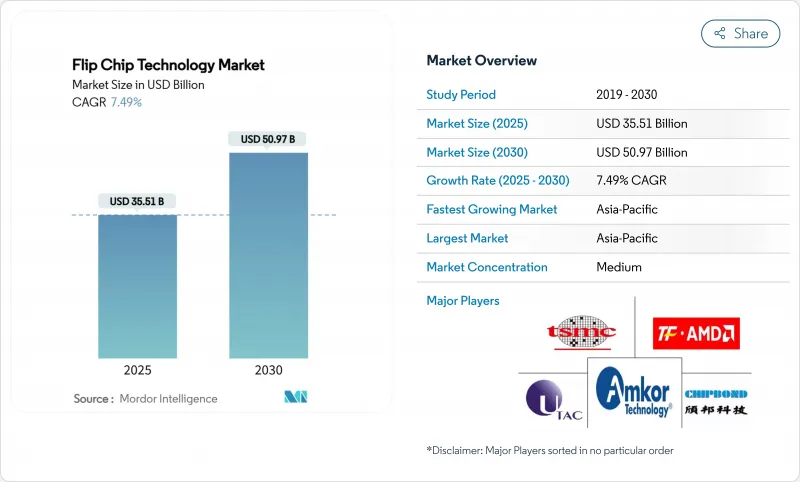
플립칩 기술 시장 규모는 2025년에 355억 1,000만 달러, 2030년에는 509억 7,000만 달러에 이를 것으로 예상되며, CAGR은 7.49%를 나타낼 전망입니다.
이 성장은 고밀도의 열 효율적인 상호 연결이 필요한 칩렛 기반 아키텍처로의 반도체 산업의 전환을 반영합니다. AI 데이터센터의 건설은 고대역폭 메모리 패키징을 전면에 밀어내고, 구리 필러나 하이브리드 본딩 라인은 기존 솔더 범프에서는 대응할 수 없었던 미세 피치의 요구에 대응했습니다. 주조 제조업체는 포장 분야에 진입하여 수직 통합을 가속화하고 외주 어셈블리 및 테스트 공급자에게 새로운 경쟁 압력을 제공했습니다. 아시아태평양은 규모의 우위를 유지하면서도 북미와 유럽공급망 리스크 경감 프로그램이 첨단 패키징 시설에 대한 대규모 그린 필드 투자의 방아쇠가 되었습니다.
세계의 플립칩 기술 시장 동향과 인사이트
이기종 통합(AI/HPC) 수요 급증
칩 제조업체는 2D 스케일링에서 복수의 칩렛을 하나의 패키지에 접합하는 이기종 집적으로 축발을 옮겨 미세 피치의 Cu-Cu 배선에 대한 수요를 밀어 올렸습니다. TSMC가 2026년까지 CoWoS 용량을 131만 단위로 강화할 계획은 Nvidia와 같은 GPU 공급업체가 플립칩 기술 시장을 어떻게 형성했는지를 보여줍니다. 이 접근법은 레거시 범프에 비해 전력 소비를 줄이면서 대역폭을 향상시키고 AI 가속기의 성능 로드맵을 지원합니다.
구리 기둥 범프와 마이크로 범프 상호 연결 채택 증가
구리 필러 범프는 뛰어난 전기 저항과 신뢰성을 실현해 2024년의 매출 점유율 46.3%를 차지했습니다. 듀폰의 고속 도금제품은 40µm 이하의 피치에 필수적인 균일한 두께 제어를 제공했습니다. 이 변화는 주석-납의 우위를 침식하고 플립칩 기술 시장을 지원하는 3D 집적 방식에 대한 길을 열었습니다.
고급 범핑 라인의 높은 자본 집약도
하위 10µm 피치로 미세화하려면 리소그래피 스테퍼, 고급 스퍼터링 도구 및 플라즈마 클리너가 필요했으며 라인 비용은 모듈당 2억 5,000만 달러를 초과했습니다. TSMC는 패키징 전용 공장에 900억 달러를 투입해 소규모 경쟁사들에게 참가의 장애물이 높다는 것을 부각하고 있습니다. 미국 JOINT 컨소시엄에 3M 참여와 같은 공동 R&D 프로그램은 공급망 전체에 위험을 분산시키는 것을 목표로 합니다.
부문 분석
2024년 플립칩 기술 시장에서 구리 기둥 기술 매출은 46.3%를 차지했습니다. 이 부문은 저항의 감소와 통전 능력의 향상으로부터 혜택을 받았습니다. Cu-to-Cu 하이브리드 본딩의 플립칩 기술 시장 규모는 칩렛 채용 증가에 따라 CAGR 9.8%를 나타낼 것으로 예측되고 있습니다. 하이브리드 방식은 칩 사이의 간격을 0.8µm까지 좁혀 솔더의 물리적 한계를 훨씬 넘어섰습니다. 주석 납 솔루션은 여전히 레거시 노드를 지원했으며 금 스터드 범프는 여전히 항공우주 분야로 제한되었습니다.
전기도금 화학의 발전으로 3D 스택의 필수 조건인 기둥 높이 균일성이 2% 이하로 유지되었습니다. IEEE 조사는 260℃에서 솔더 프리 Cu-Cu 접합이 이기종 통합의 제조가능한 경로임을 입증했습니다. 기술 혁신으로 구리 형식은 무연 및 귀금속 대체품에서 점유율을 빼앗기게 되었습니다.
FC-BGA는 서버에서 입증된 신뢰성으로 2024년 매출의 38.1%를 차지했습니다. FOWLP(Fan-Out WLP)와 패널 레벨 포맷은 큰 바디 크기를 요구하는 AI 가속기로 뒷받침되며 CAGR 10.1%를 나타낼 것으로 예측됩니다. ASE는 웨이퍼의 7배 사용 가능 면적을 약속하는 310mm X 310mm 패널에 2억 달러를 할당했습니다. 패널 레벨 패키지의 플립칩 기술 시장 규모는 라인 수율이 향상됨에 따라 상승합니다.
CoWoS 및 EMIB와 같은 특수 흐름은 AI 트레이닝 유닛에 필수적인 HBM 스태킹을 가능하게 합니다. IBM과 인텔은 유기 라미네이트보다 휨이 적고 라인 스페이스 비율이 높은 유리 기판 로드맵을 추구했습니다. TSV를 사용한 3D IC는 고비용과 공정 복잡성으로 인해 극단적인 대역폭 클래스 디바이스에서 틈새 시장을 유지했지만 달성 가능한 성능 상한을 설정했습니다.
플립칩 기술 시장은 웨이퍼 범핑 프로세스(구리 기둥, 주석-연 공정 납땜, 기타), 패키징 기술(FC-BGA, FCCSP/CSP, 기타), 제품(메모리, CMOS 이미지 센서, 기타), 최종 이용 산업(가전 및 웨어러블, 자동차 및 운송, 산업 및 로봇, 기타), 지역(북미, 남아메리카, 구, 아시아, 아시아)
지역별 분석
아시아태평양은 2024년 매출의 54.5%를 차지했습니다. 이 지역은 웨이퍼 팹의 대부분을 옹호하고 비용 우위성을 유지하고 있으며, 플립칩 기술 시장의 최대 슬라이스를 유지하고 있습니다. 정부의 우대조치가 넥스트노드의 연구개발을 지지했지만, 수출규제에 의해 대기업은 해외에 병행생산능력을 구축하게 되었습니다. 북미에서는 CHIPS법 하에서 주조와 패키징의 시작이 가속되어 탄력성이 증가하여 현지에서 수요 견인력이 탄생했습니다. 애리조나 주와 텍사스 캠퍼스가 온라인화되어 북미 플립칩 기술 시장 점유율이 소폭 상승할 것으로 예측됩니다.
유럽은 유럽 칩법을 통해 기술 주권을 추구하고 패널 레벨과 유리 코어 기판 라인에 자본을 돌렸습니다. 실리콘 박스의 노발라 공장은 2028년까지 매주 1만 장의 패널을 가공할 예정이며, 이 지역의 생태계를 지원합니다. 중동 및 아프리카는 초기 단계에 머물렀지만 전자 제품의 최종 조립 기지가 세계 공급망에 공급된다는 이점이 있습니다.
공급망의 다양화는 미래 투자를 적어도 3대륙에 분산시켜 단일 지역의 우위를 약화시키고 있습니다. 그러나 아시아태평양은 여전히 타의 추종을 불허하는 엔지니어링의 깊이를 자랑하며 대량 생산의 중심지로서의 지위를 유지하고 있습니다.
기타 혜택 :
- 엑셀 형식 시장 예측(ME) 시트
- 3개월간의 애널리스트 지원
목차
제1장 서론
- 조사 전제조건과 시장 정의
- 조사 범위
제2장 조사 방법
제3장 주요 요약
제4장 시장 상황
- 시장 개요
- 시장 성장 촉진요인
- 이기종 인테그레이션(AI/HPC) 수요의 급증
- 구리 기둥 및 마이크로 범프 상호 연결 채택 증가
- 웨어러블과 IoT의 소형화 추진
- 자동차 ADAS/EV의 신뢰성 요건
- 유리 코어 기판의 상업 시험
- 칩 레이디인 Cu-to-Cu 하이브리드 접합에 대한 수요
- 시장 성장 억제요인
- 고도의 범핑 라인의 높은 자본 집약도
- 무연의 신뢰성과 휨의 과제
- 10μm 이하의 얼라인먼트 수율 손실
- 중요 금속화학제품 공급망
- 밸류체인 분석
- 거시경제 요인의 영향
- 규제 상황
- 기술의 전망
- Porter's Five Forces
- 공급기업의 협상력
- 구매자의 협상력
- 신규 참가업체의 위협
- 대체품의 위협
- 경쟁 기업 간 경쟁 관계
- 투자분석
제5장 시장 규모와 성장 예측
- 웨이퍼 범핑 프로세스별
- 구리 필러
- 주석 납 공융 솔더
- 무연 솔더(SnAg, SAC 등)
- 금 스터드 범핑
- 구리-구리 하이브리드/직접 본딩
- 포장 기술별
- FC-BGA(2D/2.1D/2.5D/3D)
- FCCSP/CSP
- CoWoS/InFO/EMIB
- FOWLP(팬아웃 WLP)/PLP
- TSV 부착 3D IC
- 제품별
- 메모리(DRAM, HBM)
- CMOS 이미지 센서
- LED 및 미니/마이크로 LED
- SoC/애플리케이션 프로세서
- GPU/AI 가속기
- CPU/서버 프로세서
- 최종 이용 산업별
- 소비자 가전 및 웨어러블
- 자동차 및 운송
- 산업 및 로봇공학
- 통신 및 5G 인프라
- 데이터센터 및 클라우드
- 군사 및 항공우주
- 의료 및 헬스케어 기기
- 지역별
- 북미
- 미국
- 캐나다
- 멕시코
- 남미
- 브라질
- 기타 남미
- 유럽
- 독일
- 프랑스
- 영국
- 러시아
- 기타 유럽
- 아시아태평양
- 중국
- 대만
- 한국
- 일본
- 말레이시아
- 싱가포르
- 기타 아시아태평양
- 중동 및 아프리카
- 중동
- 튀르키예
- 기타 중동
- 아프리카
- 남아프리카
- 기타 아프리카
- 북미
제6장 경쟁 구도
- 시장 집중도
- 전략적인 동향(M&A, 합작투자, 생산능력 확장)
- 시장 점유율 분석
- 기업 프로파일
- Amkor Technology, Inc.
- ASE Technology Holding Co., Ltd.
- Taiwan Semiconductor Manufacturing Company Limited
- Jiangsu Changjiang Electronics Technology Co., Ltd.
- Powertech Technology Inc.
- Chipbond Technology Corporation
- UTAC Holdings Ltd.
- TF-AMD Microelectronics Sdn. Bhd.
- Shinko Electric Industries Co., Ltd.
- Unisem(M) Berhad
- Hana Micron Inc.
- Nepes Corporation
- Carsem(M) Sdn. Bhd.
- Sigurd Microelectronics Corporation
- AT&S Austria Technologie & Systemtechnik AG
- Intel Corporation
- Samsung Electronics Co., Ltd.
- Advanced Micro Devices, Inc.
- Texas Instruments Incorporated
- United Microelectronics Corporation
- STATS ChipPAC Pte. Ltd.
- SFA Semicon Co., Ltd.
- Tongfu Microelectronics Co., Ltd.
- Huatian Technology Co., Ltd.
- Lingsen Precision Industries, Ltd.
제7장 시장 기회와 향후 전망
KTH 25.11.13The flip chip technology market size stood at USD 35.51 billion in 2025 and is on track to reach USD 50.97 billion by 2030, reflecting a 7.49% CAGR.

Growth mirrored the semiconductor industry's transition to chiplet-based architectures that required dense, thermally efficient interconnects. AI data-center build-outs pushed high-bandwidth memory packaging to the fore, while copper-pillar and hybrid bonding lines addressed the fine-pitch needs that traditional solder bumps could not meet. Foundries entered the packaging arena, accelerating vertical integration and bringing new competitive pressures on outsourced assembly and test providers. Asia-Pacific retained scale advantages, yet supply-chain de-risking programs in North America and Europe triggered large green-field investments in advanced packaging facilities.
Global Flip Chip Technology Market Trends and Insights
Surge in Heterogeneous Integration Demand (AI/HPC)
Chipmakers pivoted from 2D scaling to heterogeneous integration that joined multiple chiplets in a single package, lifting demand for fine-pitch Cu-to-Cu interconnects. TSMC's plan to boost CoWoS capacity to 1.31 million units by 2026 illustrated how GPU vendors such as Nvidia shaped the flip chip technology market. The approach enhanced bandwidth while lowering power compared with legacy bumps, supporting the performance roadmap for AI accelerators.
Rising Adoption of Copper-Pillar and Micro-Bump Interconnects
Copper-pillar bumps delivered superior electrical resistance and reliability, explaining their 46.3% 2024 revenue share. High-speed plating chemistries from DuPont provided uniform thickness control essential for sub-40 µm pitches. The shift eroded tin-lead dominance and paved the way for 3D integration schemes that underpin the flip chip technology market.
High Capital Intensity of Advanced Bumping Lines
Scaling to sub-10 µm pitches required lithography steppers, advanced sputter tools, and plasma cleaners that pushed line cost above USD 250 million per module. TSMC earmarked USD 90 billion for dedicated packaging plants, underscoring the entry hurdle for smaller competitors. Collaborative R&D programs such as 3M's participation in the US-JOINT consortium aimed to spread risk across the supply chain.
Other drivers and restraints analyzed in the detailed report include:
- Wearables and IoT Miniaturization Push
- Automotive ADAS/EV Reliability Requirements
- Lead-Free Reliability and Warpage Challenges
For complete list of drivers and restraints, kindly check the Table Of Contents.
Segment Analysis
Copper pillar technology held 46.3% revenue in 2024 within the flip chip technology market. The segment benefited from reduced resistance and heightened current-carrying capability. The flip chip technology market size for Cu-to-Cu hybrid bonding is projected to expand at a 9.8% CAGR as chiplet adoption grows. The hybrid method lowered inter-chip spacing to 0.8 µm, far beyond solder's physical limits. Tin-lead solutions still served legacy nodes, whereas gold-stud bumps remained confined to aerospace.
Advances in electroplated chemistries sustained pillar height uniformity below 2%, a prerequisite for 3D stacks. IEEE research validated solder-free Cu-Cu bonding at 260 °C as a manufacturable path for heterogeneous integration. Innovations positioned copper formats to absorb share from both lead-free and precious-metal alternatives.
FC-BGA commanded 38.1% of 2024 revenue thanks to proven reliability in servers. Fan-out WLP and panel-level formats are expected to record a 10.1% CAGR, catalyzed by AI accelerators demanding large body sizes. ASE allocated USD 200 million to 310 mm X 310 mm panels that promise sevenfold usable area over wafers, a cost breakthrough. The flip chip technology market size for panel-level packages will climb as line yields improve.
Specialty flows such as CoWoS and EMIB enable HBM stacking essential for AI training units. IBM and Intel pursued glass-substrate roadmaps that offer lower warpage and higher line-space ratios than organic laminates. 3D IC with TSV remained a niche for extreme bandwidth-class devices due to high cost and process complexity, but set the ceiling on attainable performance.
Flip Chip Technology Market is Segmented by Wafer Bumping Process (Copper Pillar, Tin-Lead Eutectic Solder, and More), Packaging Technology (FC-BGA, FCCSP/CSP, and More), Product (Memory, CMOS Image Sensor, and More), End-Use Industry (Consumer Electronics and Wearables, Automotive and Transportation, Industrial and Robotics, and More), and Geography (North America, South America, Europe, Asia-Pacific, and Middle East and Africa).
Geography Analysis
Asia-Pacific held 54.5% of 2024 revenue. The region housed the bulk of wafer fabs and retained cost advantages, sustaining the largest slice of the flip chip technology market. Government incentives supported next-node R&D, yet export-control actions induced leading firms to build parallel capacity offshore. North America accelerated foundry and packaging startups under the CHIPS Act, adding resilience and creating a local demand pull. The flip chip technology market share for North America is expected to rise modestly as Arizona and Texas campuses come online.
Europe pursued technology sovereignty through the European Chips Act and directed capital toward panel-level and glass-core substrate lines. Silicon Box's Novara facility is slated to process 10,000 panels weekly by 2028, anchoring a regional ecosystem. Middle East and Africa remained early-stage but benefited from electronics final-assembly hubs that feed into global supply chains.
Supply-chain diversification scattered future investments across at least three continents, muting single-region dominance. However, Asia-Pacific still boasted unmatched engineering depth, keeping it the reference center for high-volume manufacturing.
- Amkor Technology, Inc.
- ASE Technology Holding Co., Ltd.
- Taiwan Semiconductor Manufacturing Company Limited
- Jiangsu Changjiang Electronics Technology Co., Ltd.
- Powertech Technology Inc.
- Chipbond Technology Corporation
- UTAC Holdings Ltd.
- TF-AMD Microelectronics Sdn. Bhd.
- Shinko Electric Industries Co., Ltd.
- Unisem (M) Berhad
- Hana Micron Inc.
- Nepes Corporation
- Carsem (M) Sdn. Bhd.
- Sigurd Microelectronics Corporation
- AT&S Austria Technologie & Systemtechnik AG
- Intel Corporation
- Samsung Electronics Co., Ltd.
- Advanced Micro Devices, Inc.
- Texas Instruments Incorporated
- United Microelectronics Corporation
- STATS ChipPAC Pte. Ltd.
- SFA Semicon Co., Ltd.
- Tongfu Microelectronics Co., Ltd.
- Huatian Technology Co., Ltd.
- Lingsen Precision Industries, Ltd.
Additional Benefits:
- The market estimate (ME) sheet in Excel format
- 3 months of analyst support
TABLE OF CONTENTS
1 INTRODUCTION
- 1.1 Study Assumptions and Market Definition
- 1.2 Scope of the Study
2 RESEARCH METHODOLOGY
3 EXECUTIVE SUMMARY
4 MARKET LANDSCAPE
- 4.1 Market Overview
- 4.2 Market Drivers
- 4.2.1 Surge in heterogeneous integration demand (AI/ HPC)
- 4.2.2 Rising adoption of copper-pillar and micro-bump interconnects
- 4.2.3 Wearables and IoT miniaturization push
- 4.2.4 Automotive ADAS/EV reliability requirements
- 4.2.5 Glass-core substrate commercial trials
- 4.2.6 Demand for chip-let-ready Cu-to-Cu hybrid bonding
- 4.3 Market Restraints
- 4.3.1 High capital intensity of advanced bumping lines
- 4.3.2 Lead-free reliability and warpage challenges
- 4.3.3 Sub-10 µm alignment yield losses
- 4.3.4 Supply-chain exposure to critical metal chemicals
- 4.4 Value Chain Analysis
- 4.5 Impact of Macroeconomic Factors
- 4.6 Regulatory Landscape
- 4.7 Technological Outlook
- 4.8 Porter's Five Forces
- 4.8.1 Bargaining Power of Suppliers
- 4.8.2 Bargaining Power of Buyers
- 4.8.3 Threat of New Entrants
- 4.8.4 Threat of Substitutes
- 4.8.5 Intensity of Competitive Rivalry
- 4.9 Investment Analysis
5 MARKET SIZE AND GROWTH FORECASTS (VALUE)
- 5.1 By Wafer Bumping Process
- 5.1.1 Copper Pillar
- 5.1.2 Tin-Lead Eutectic Solder
- 5.1.3 Lead-Free Solder (SnAg, SAC, etc.)
- 5.1.4 Gold-Stud Bumping
- 5.1.5 Cu-to-Cu Hybrid / Direct Bond
- 5.2 By Packaging Technology
- 5.2.1 FC-BGA (2D/2.1D/2.5D/3D)
- 5.2.2 FCCSP / CSP
- 5.2.3 CoWoS / InFO / EMIB
- 5.2.4 Fan-Out WLP / PLP
- 5.2.5 3D IC with TSV
- 5.3 By Product
- 5.3.1 Memory (DRAM, HBM)
- 5.3.2 CMOS Image Sensor
- 5.3.3 LED and Mini/Micro-LED
- 5.3.4 SoC / Application Processor
- 5.3.5 GPU / AI Accelerator
- 5.3.6 CPU / Server Processor
- 5.4 By End-Use Industry
- 5.4.1 Consumer Electronics and Wearables
- 5.4.2 Automotive and Transportation
- 5.4.3 Industrial and Robotics
- 5.4.4 Telecommunications and 5G Infrastructure
- 5.4.5 Data Center and Cloud
- 5.4.6 Military and Aerospace
- 5.4.7 Medical and Healthcare Devices
- 5.5 By Geography
- 5.5.1 North America
- 5.5.1.1 United States
- 5.5.1.2 Canada
- 5.5.1.3 Mexico
- 5.5.2 South America
- 5.5.2.1 Brazil
- 5.5.2.2 Rest of South America
- 5.5.3 Europe
- 5.5.3.1 Germany
- 5.5.3.2 France
- 5.5.3.3 United Kingdom
- 5.5.3.4 Russia
- 5.5.3.5 Rest of Europe
- 5.5.4 Asia-Pacific
- 5.5.4.1 China
- 5.5.4.2 Taiwan
- 5.5.4.3 South Korea
- 5.5.4.4 Japan
- 5.5.4.5 Malaysia
- 5.5.4.6 Singapore
- 5.5.4.7 Rest of Asia-Pacific
- 5.5.5 Middle East and Africa
- 5.5.5.1 Middle East
- 5.5.5.1.1 Turkey
- 5.5.5.1.2 Rest of Middle East
- 5.5.5.2 Africa
- 5.5.5.2.1 South Africa
- 5.5.5.2.2 Rest of Africa
- 5.5.1 North America
6 COMPETITIVE LANDSCAPE
- 6.1 Market Concentration
- 6.2 Strategic Moves (M&A, JV, Capacity Expansions)
- 6.3 Market Share Analysis
- 6.4 Company Profiles (includes Global-level Overview, Market-level Overview, Core Segments, Financials, Strategic Information, Market Rank/Share, Products and Services, Recent Developments)
- 6.4.1 Amkor Technology, Inc.
- 6.4.2 ASE Technology Holding Co., Ltd.
- 6.4.3 Taiwan Semiconductor Manufacturing Company Limited
- 6.4.4 Jiangsu Changjiang Electronics Technology Co., Ltd.
- 6.4.5 Powertech Technology Inc.
- 6.4.6 Chipbond Technology Corporation
- 6.4.7 UTAC Holdings Ltd.
- 6.4.8 TF-AMD Microelectronics Sdn. Bhd.
- 6.4.9 Shinko Electric Industries Co., Ltd.
- 6.4.10 Unisem (M) Berhad
- 6.4.11 Hana Micron Inc.
- 6.4.12 Nepes Corporation
- 6.4.13 Carsem (M) Sdn. Bhd.
- 6.4.14 Sigurd Microelectronics Corporation
- 6.4.15 AT&S Austria Technologie & Systemtechnik AG
- 6.4.16 Intel Corporation
- 6.4.17 Samsung Electronics Co., Ltd.
- 6.4.18 Advanced Micro Devices, Inc.
- 6.4.19 Texas Instruments Incorporated
- 6.4.20 United Microelectronics Corporation
- 6.4.21 STATS ChipPAC Pte. Ltd.
- 6.4.22 SFA Semicon Co., Ltd.
- 6.4.23 Tongfu Microelectronics Co., Ltd.
- 6.4.24 Huatian Technology Co., Ltd.
- 6.4.25 Lingsen Precision Industries, Ltd.
7 MARKET OPPORTUNITIES AND FUTURE OUTLOOK
- 7.1 White-space and Unmet-Need Assessment
