
|
시장보고서
상품코드
2044017
디스크리트 디바이스용 실리콘 웨이퍼 : 시장 점유율 분석, 업계 동향 및 통계, 성장 예측(2026-2031년)Silicon Wafer For Discrete Devices - Market Share Analysis, Industry Trends & Statistics, Growth Forecasts (2026 - 2031) |
||||||
 Mordor Intelligence
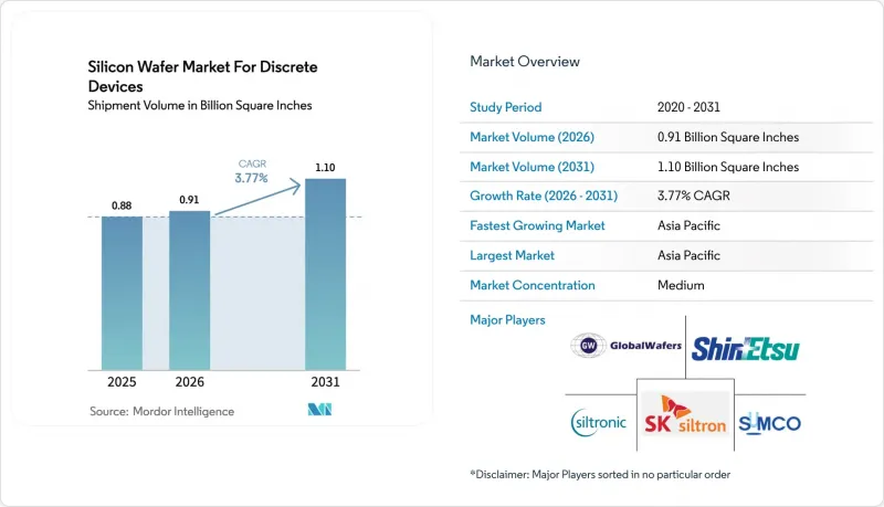
디스크리트 디바이스용 실리콘 웨이퍼 시장 규모는 2025년에 8억 8,000만 평방인치로 평가되었습니다. 2026년 9억 1,000만 평방인치에서 2031년까지 11억 평방인치에 이를 것으로 예상되며, 예측 기간(2026-2031년) CAGR은 3.77%를 나타낼 전망입니다.
배터리 전기자동차, 재생에너지용 인버터, 공장자동화용 드라이브는 기존 가전제품보다 높은 정격전류를 필요로 하기 때문에 전력용 기판으로 수요가 이동하고 있습니다. 미국의 'CHIPS and Science Act', 유럽의 'Chips Act', 중국의 '3차 집적회로 기금'에 따른 정부 보조금으로 인해 200mm 라인 증설이 가속화되고 있으며, 설비 투자 회수 기간이 단축되고 공급업체 간 경쟁이 심화되고 있습니다. 2025년 초 폴리실리콘 현물 가격이 1kg당 8-9달러까지 회복되면서 웨이퍼 공급업체들이 장기 계약에 지수 연동형 에스컬레이터 조항을 포함시키면서 수익률에 변동이 생겼습니다. 현재 자동차의 전동화가 기판 배분을 주도하고 있으며, 배터리 전기자동차 플랫폼의 차량 1대당 개별 부품 수는 3배 이상 증가한 1,200개 이상으로 증가하였습니다. 또한, 산업용 모터 구동장치의 개조가 수량 성장의 두 번째 구조적 지주가 되고 있습니다. 동시에 중국으로의 첨단 증착 및 리소그래피 장비의 수출을 제한하는 규제로 인해 공급망이 양극화되어 중국 이외의 구매자에게는 리드타임이 길어지고 있습니다. 이에 따라 다국적 OEM 업체들은 지역을 넘나드는 웨이퍼의 듀얼 소싱을 추진하고 있습니다.
디스크리트 디바이스용 실리콘 웨이퍼 시장 동향과 전망
고전류 다이오드를 필요로 하는 EV 급속 충전 인프라 확대 필요
현재 중국, 유럽, 미국의 고속도로 연선에는 350kW급 초고속 충전기가 주류를 이루고 있으며, 각 설치 지점에서 정격 1,200-1,700볼트, 100암페어 이상의 이산 다이오드가 8-12개씩 소비되고 있습니다. Wolfspeed는 2025년 2월에 이러한 정류단용 200mm SiC-on-silicon 에피택셜 플랫폼을 출시하여 서지 전류 요구사항이 증가함에 따라 웨이퍼의 휨, 왜곡, 결함 밀도 등 웨이퍼의 지표가 얼마나 엄격해져야 하는지를 입증했습니다. 얼마나 더 엄격해져야 하는지를 보여주었습니다. 중국 국가전력망은 2025년까지 12만 개의 초급속 충전기를 증설했으며, 이로 인해 약 1,500만-2,000만 평방인치의 고전류 다이오드용 기판에 대한 추가 수요가 발생했습니다. 유럽연합(EU)의 '대체연료 인프라 규정'에 따라 2027년까지 상호 운용 가능한 충전 네트워크 구축이 의무화되어 있으며, 이산소자를 많이 사용하는 CCS(Combined Charging System) 프로토콜이 정착될 것입니다. 50kHz 이상의 높은 스위칭 주파수로 인해 고저항 실리콘 위에 SiC 쇼트키 다이오드에 대한 선호도가 높아지고 있으며, 이러한 추세로 인해 프라임 연마 등급보다 특수 기판의 출하량이 증가하고 있습니다.
GaN/SiC 하이브리드 모듈 채택으로 고저항 실리콘 기판 수요 증가
고저항 실리콘에 GaN HEMT와 SiC 다이오드를 공동 밀봉한 하이브리드 전력 모듈은 모놀리식 SiC에 비해 와트당 비용을 30-40% 절감하여 자동차 제조업체가 와트당 0.15달러의 시스템 목표를 달성할 수 있게 해줍니다. 2024년 3월에 출시된 인피니언의 CoolSiC 디바이스는 이 아키텍처를 채택하고 있으며, 이미 1,000-10,000 옴-센티미터로 규정된 200mm 웨이퍼로 출하되고 있습니다. ST마이크로일렉트로닉스는 2024년 하이브리드 모듈 매출이 28% 증가했다고 보고했으며, 판매량의 65%가 자동차 제조업체를 대상으로 한 것으로 나타나 이러한 기판의 상업적 모멘텀을 뒷받침하고 있습니다. 일본 경제산업성은 2025년도에 고저항 실리콘의 국내 생산을 지원하기 위해 450억 엔(3억 7,000만 달러)을 책정하여 국가 정책을 자동차 파워일렉트로닉스와 명확하게 연결시켰습니다. 650V 디바이스용 실리콘 웨이퍼 상의 GaN(GaN on silicon)은 111 결정방위가 10^6 cm-2 미만의 나사산 전위 밀도를 필요로 하는데, 특수 웨이퍼 공급업체만이 이 요건을 충족할 수 있어 공급망 진입장벽이 높아지고 있습니다.
폴리실리콘 가격 변동과 에너지 비용
폴리실리콘 가격은 2022년부터 2025년까지 1kg당 6달러에서 35달러까지 변동했습니다. 2025년 초 현물 가격은 1kg당 8-9달러까지 회복된 반면, 장기 계약 가격은 11-13달러에 머물러 일반 웨이퍼의 수익률을 압박하고 있습니다. 유럽 생산자들은 2019년의 3배에 달하는 kW시당 평균 0.18유로(kW시당 0.20달러)의 전기요금에 직면하고 있으며, 결정 성장에 잉곳 1kg당 약 225 kW시의 전력을 소비하기 때문에 그 영향은 더욱 확대되고 있습니다. 더욱 확대되고 있습니다. 중국 각 성에서는 kW시당 0.35위안(0.05달러)의 낮은 수준의 산업 보조금을 통해 에너지 집약도를 상쇄하고 있는 반면, 미국의 인플레이션 억제법(Inflation Reduction Act)에서는 청정에너지 사용에 대해 kW시당 0.03달러의 생산세 공제를 적용하고 있습니다. kW시당 0.03달러의 생산 세액공제가 적용됩니다. 5개 폴리실리콘 벤더공급 집중으로 가격 변동성이 확대되고 있으며, 웨이퍼 공급업체는 가격 전가 조항을 계약서에 포함시키거나 가격 급등 시 마이너스 총이익률을 감수할 수밖에 없는 상황입니다.
부문 분석
2025년 기준, 200mm 슬라이스는 감가상각이 완료된 팹 자산에 힘입어 실리콘 웨이퍼 시장 점유율의 59.66%를 차지했습니다. 이러한 자산은 개별 트랜지스터와 다이오드에서 여전히 최고의 비용 효율성을 유지하고 있습니다. 일본, 체코, 말레이시아에 위치한 자동차 인증 팹은 90% 이상의 가동률을 유지하고 있습니다. 이 직경은 처리량과 제품 구성의 유연성 사이의 균형을 최적화하기 때문입니다. 300mm 기판은 실리콘 웨이퍼 시장 규모의 24%에 불과하지만, 집적형 전력 관리 IC와 멀티칩 아날로그 모듈이 리소그래피 오버헤드를 수백 개의 다이에 분산시키기 위해 대형 웨이퍼로 이동함에 따라 2031년까지 연평균 4.52%의 성장률을 나타낼 것으로 예측됩니다. 텍사스 기기는 리처드슨 공장 생산량의 40%를 아날로그 및 전력 제품에 투입할 계획이며, 이는 300mm 공급에 대한 수요를 뒷받침할 것입니다.
최대 150mm급 웨이퍼는 특수한 결정방위가 소형화를 정당화하는 틈새 시장인 RF 다이오드, 사이리스터, 센서 시장에서 여전히 존재합니다. SEMI는 2028년까지 전체 반도체 부문의 200mm 웨이퍼 출하량이 연간 1.2% 감소할 것으로 예상하고 있지만, 메모리 및 MCU 생산으로 인한 여유 생산능력을 디스크리트 디바이스 수요가 부분적으로 상쇄할 것으로 전망하고 있습니다. 또한, 공급망 탄력성에 대한 우려로 자동차 업체들은 200mm 웨이퍼의 조달처를 일본과 중국으로 분산하는 움직임을 보이고 있으며, 지진과 지정학적 리스크에 대한 지역적 리스크 헤지를 위해 노력하고 있습니다.
'디스크리트 디바이스용 실리콘 웨이퍼 시장 보고서'는 웨이퍼 직경(150mm 이하, 200mm, 300mm), 웨이퍼 유형(프라임 폴리싱, 에피택셜, SOI, 특수 실리콘), 최종 사용자(가전, 산업용, 통신, 자동차 등), 지역(북미, 유럽, 아시아태평양 등)별로 분류하여 분석하였습니다. 북미, 유럽, 아시아태평양 등)로 분류되어 있습니다. 시장 예측은 수량(평방인치) 기준으로 제공됩니다.
지역별 분석
아시아태평양은 2025년 출하량의 81.84%를 차지했으며, 일본, 대만, 중국이 200mm 웨이퍼 생산 능력을 확대함에 따라 2031년까지 연평균 복합 성장률(CAGR) 4.79%를 나타낼 것으로 예측됩니다. 신에츠화학과 SUMCO는 2024년 총 4억 5,000만 평방인치 이상을 출하했습니다. 양사는 저항률의 균일성을 ±5% 이내로 유지하는 독자적인 초크랄스키 공법을 활용하고 있습니다. 대만의 GlobalWafers는 2024년 생산량의 35%를 개별 고객에게 할당하고, 온세미컨덕터 및 비샤이와의 장기 계약을 활용하여 가동률을 85% 이상으로 유지했습니다. 중국 공급업체인 NSIG와 Zhonghuan은 2024년부터 2025년까지 80억 위안(11억 달러)의 보조금을 지원받아 200mm 생산능력을 8,000만 평방인치로 확대했습니다.
2025년에는 북미가 8%를 차지했습니다. CHIPS 법에 따른 4억 달러의 자금은 GlobalWafers의 텍사스주 신규 팹을 지원하며, 이 팹은 2027년 이후 300mm 웨이퍼 생산량의 40%를 파워 디스크리트용으로 확보할 예정입니다. 미시간 주에 위치한 Hemlock Semiconductor의 3억 2,500만 달러 규모의 폴리실리콘 확장 계획은 업스트림 공급의 현지화를 더욱 촉진하고 미국 웨이퍼 생산 라인을 중국의 원자재 위험으로부터 분리하는 것이지만, 생산 확장은 2029년까지 완료되지 않을 것입니다.
유럽은 생산량의 6%를 차지하고 있으며, 실트로닉 AG와 소이텍이 에피택셜 및 SOI 라인을 통해 독일과 프랑스의 자동차 산업 거점에 공급하고 있습니다. '유럽 공동 이익 중요 프로젝트(IPEC)'의 승인으로 ST마이크로일렉트로닉스, 인피니언, 온세미컨덕터를 지원하는 파워디스크리트용 파일럿 라인에 7억 유로(7억 9,100만 달러)가 투입됐지만, 2028년 이전에 양산이 시작될 가능성은 낮다고 합니다. 낮게 보고 있습니다. 남미, 중동, 아프리카를 합해도 5% 미만이며, 조립 및 테스트 시설에서는 수입 웨이퍼에 의존하고 있습니다.
웨이퍼 생산이 대만 서해안에서 100km 이내에 집중되어 있기 때문에 실리콘 웨이퍼 시장은 지진과 지정학적 혼란의 영향을 받기 쉽습니다. 자동차 OEM 업체들은 단일 장애 지점(SPOF) 리스크를 줄이기 위해 일본과 대만공급처와 미국 및 유럽의 백업 생산 능력을 결합한 '듀얼 리저널 소싱'을 점점 더 많이 요구하고 있습니다.
기타 혜택 :
- 엑셀 형식 시장 예측(ME) 시트
- 3개월간 애널리스트 지원
자주 묻는 질문
목차
제1장 서론
제2장 조사 방법
제3장 주요 요약
제4장 시장 구도
제5장 시장 규모와 성장 예측
제6장 경쟁 구도
제7장 시장 기회와 향후 전망
KTH 26.05.29The silicon wafer market size for discrete devices was valued at 0.88 billion square inches in 2025 and is estimated to grow from 0.91 billion square inches in 2026 to reach 1.10 billion square inches by 2031, at a CAGR of 3.77% during the forecast period (2026-2031).
Demand pivots toward power-oriented substrates as battery-electric vehicles, renewable-energy inverters, and factory-automation drives require higher current ratings than legacy consumer electronics. Government subsidies under the United States CHIPS and Science Act, the European Chips Act, and China's third Integrated Circuit Fund are accelerating 200 millimeter line additions, compressing equipment payback periods and intensifying supplier competition. Polysilicon spot-price recovery to USD 8-9 per kilogram in early 2025 injected margin volatility, prompting wafer suppliers to embed index-based escalators in long-term contracts. Automotive electrification now anchors substrate allocation, with per-vehicle discrete content tripling to more than 1 200 units in battery-electric platforms, and industrial-motor-drive retrofits add a second structural leg to volume growth. Simultaneously, export-control regimes that restrict advanced deposition and lithography tools to China are bifurcating supply chains, extending lead times for non-Chinese buyers, and motivating multinational OEMs to dual-source wafers across regions.
Insights and Trends of Silicon Wafer Market For Discrete Devices
Expansion Of EV Fast-Charging Infrastructure Requiring High-Current Diodes
Ultra-fast chargers rated at 350 kilowatts now dominate highway corridors in China, Europe, and the United States, and each installation consumes 8-12 discrete diodes rated for 1 200-1 700 volts and more than 100 amperes. Wolfspeed unveiled a 200 millimeter SiC-on-silicon epitaxial platform in February 2025 that targets these rectifier stages and demonstrates how wafer metrics such as bow, warp, and defect density must tighten when surge-current requirements rise. China's State Grid added 120 000 ultra-fast chargers in 2025, translating to incremental demand for roughly 15-20 million square inches of high-current-diode substrates. The European Union's Alternative Fuels Infrastructure Regulation mandates interoperable charging networks by 2027, locking in discrete-heavy Combined Charging System protocols. Higher switching frequencies above 50 kilohertz are shifting preference toward SiC Schottky diodes on high-resistivity silicon, a trend that lifts specialty-substrate volumes ahead of prime polished grades.
Adoption Of GaN/SiC Hybrid Modules Increasing Demand For High-Resistivity Silicon Substrates
Hybrid power modules that co-package GaN HEMTs with SiC diodes on high-resistivity silicon offer cost-per-watt metrics 30-40% below monolithic SiC, enabling automakers to meet USD 0.15 per watt system targets. Infineon's CoolSiC devices, released in March 2024, ride this architecture and already ship on 200 millimeter wafers specified at 1 000-10 000 ohm-centimeters. STMicroelectronics reported a 28% revenue jump in hybrid modules during 2024, with 65% of units sold to automotive customers, underscoring the commercial traction of these substrates. Japan's Ministry of Economy, Trade and Industry allocated JPY 45 billion (USD 307 million) in fiscal 2025 to subsidize domestic production of high-resistivity silicon, explicitly linking national policy to automotive power electronics. GaN on silicon for 650 volt devices requires 111 crystal orientation with threading-dislocation density under 10^6 cm-2, capabilities delivered only by specialty-wafer suppliers, reinforcing supply-chain entry barriers.
Price Volatility Of Polysilicon And Energy Costs
Polysilicon prices swung from USD 6 to USD 35 per kilogram between 2022 and 2025, and although early-2025 spot levels rebounded to USD 8-9 per kilogram, long-term contracts hover at USD 11-13, squeezing merchant wafer margins. European producers face electricity tariffs averaging EUR 0.18 per kilowatt-hour (USD 0.20 per kilowatt-hour), triple 2019 levels, and crystal growth consumes roughly 225 kilowatt-hours per kilogram of ingot, magnifying exposure. Chinese provinces offset energy intensity with subsidized industrial rates as low as CNY 0.35 per kilowatt-hour (USD 0.05), while the United States Inflation Reduction Act's production credit refunds USD 0.03 per kilowatt-hour for clean-energy use. Supply concentration among five polysilicon vendors amplifies volatility, forcing wafer suppliers to incorporate pass-through clauses or risk negative gross margins during spikes.
Other drivers and restraints analyzed in the detailed report include:
- Government Incentives For Domestic Discrete Component Manufacturing
- Mature Power Semiconductor Replacement With High-Voltage Discrete Devices
- Prolonged Downcycles In Consumer Electronics Affecting Low-Power Discrete Consumption
For complete list of drivers and restraints, kindly check the Table Of Contents.
Segment Analysis
The 200 millimeter slice held 59.66% of the silicon wafer market share in 2025, anchored by fully depreciated fab assets whose cost-per-die remains unbeatable for discrete transistors and diodes. Automotive-qualified fabs in Japan, Czech Republic, and Malaysia run 90%-plus utilization because this diameter balances throughput with product-mix flexibility. 300 millimeter substrates account for only 24% of the silicon wafer market size but are forecast to grow 4.52% annually through 2031 as integrated power-management ICs and multi-chip analog modules migrate to larger wafers to spread lithography overhead across hundreds of die. Texas Instruments will dedicate 40% of its Richardson Fab output to analog and power, backstopping demand for 300 millimeter supply.
The up-to-150 millimeter tier persists in niche RF-diode, thyristor, and sensor markets where exotic crystal orientations justify smaller diameters. SEMI projects 200 millimeter shipments across all semiconductor segments to decline 1.2% annually through 2028, yet discrete-device demand partially offsets this bleed by absorbing capacity vacated by memory and MCU production. Supply-chain resiliency concerns are also pushing automotive OEMs to dual-source 200 millimeter wafers from both Japan and China, creating regional hedges against seismic or geopolitical events.
The Silicon Wafer Market for Discrete Devices Report is Segmented by Wafer Diameter (Up To 150mm, 200mm, and 300mm), Wafer Type (Prime Polished, Epitaxial, Silicon-On-Insulator, and Specialty Silicon), End-User (Consumer Electronics, Industrial, Telecommunications, Automotive, and More), and Geography (North America, Europe, Asia-Pacific, and More). The Market Forecasts are Provided in Terms of Volume (Square Inches).
Geography Analysis
Asia-Pacific commanded 81.84% of 2025 volume and is expected to grow at a 4.79% CAGR through 2031 as Japan, Taiwan, and China scale 200 millimeter capacity. Shin-Etsu Chemical and SUMCO shipped more than 450 million square inches combined in 2024, leveraging proprietary Czochralski techniques for resistivity uniformity within +-5%. Taiwan's GlobalWafers dedicated 35% of 2024 output to discrete customers, using long-term contracts with onsemi and Vishay to run utilization above 85%. Chinese suppliers NSIG and Zhonghuan added 80 million square inches of 200 millimeter capacity during 2024-2025, bolstered by CNY 8 billion (USD 1.1 billion) in provincial subsidies.
North America accounted for 8% in 2025. CHIPS Act funding of USD 400 million is underwriting GlobalWafers' new Texas fab that will reserve 40% of its 300 millimeter output for power discretes starting 2027. Hemlock Semiconductor's USD 325 million polysilicon expansion in Michigan further localizes upstream supply and insulates U.S. wafer lines from Chinese feedstock risk, though ramp will not complete until 2029.
Europe held 6% of output, with Siltronic AG and Soitec serving automotive hubs in Germany and France via epitaxial and SOI lines. Important Project of Common European Interest approval enabled EUR 700 million (USD 791 million) for a power-discrete pilot line supporting STMicroelectronics, Infineon, and onsemi, but commercial production is unlikely before 2028. South America and the Middle East and Africa combined for less than 5%, relying on imported wafers for assembly and test facilities.
The heavy concentration of substrate production within 100 kilometers of Taiwan's west coast exposes the silicon wafer market to earthquake and geopolitical disruptions. Automotive OEMs increasingly mandate dual-regional sourcing, pairing Japanese or Taiwanese supply with backup capacity in the United States or Europe to mitigate single-point-of-failure risk.
- Shin-Etsu Chemical Co Ltd
- SUMCO Corporation
- GlobalWafers Co Ltd
- Siltronic AG
- SK siltron Co Ltd
- Soitec SA
- Wafer Works Corporation
- Okmetic Oy
- National Silicon Industry Group Co Ltd
- Hangzhou Semiconductor Wafer Co Ltd
- Beijing ESWIN Semiconductor Technology Co Ltd
- Ferrotec Holdings Corporation
- Hebei Puxing Electronic Technology Co Ltd
- Fujian Jinghui Semiconductor Co Ltd
- Wafertech International
- Mitsubishi Materials Corporation
- Topsil Semiconductor Materials A/S
- Zhonghuan Advanced Semiconductor Materials Co
- Tianjin Huanou International Silicon Technology
- Linton Crystal Technologies
- Siltronix ST
- GRINM Semiconductor Materials Co Ltd
- Zhejiang Jinruihong Technology Co Ltd
Additional Benefits:
- The market estimate (ME) sheet in Excel format
- 3 months of analyst support
TABLE OF CONTENTS
1 INTRODUCTION
- 1.1 Study Assumptions and Market Definition
- 1.2 Scope of the Study
2 RESEARCH METHODOLOGY
3 EXECUTIVE SUMMARY
4 MARKET LANDSCAPE
- 4.1 Market Overview
- 4.2 Industry Value Chain Analysis
- 4.3 Regulatory Landscape
- 4.4 Impact of Macroeconomic Factors
- 4.5 Porter's Five Forces Analysis
- 4.5.1 Bargaining Power of Suppliers
- 4.5.2 Bargaining Power of Buyers
- 4.5.3 Threat of New Entrants
- 4.5.4 Threat of Substitutes
- 4.5.5 Intensity of Competitive Rivalry
- 4.6 Market Drivers
- 4.6.1 Mature Power Semiconductor Replacement with High-Voltage Discrete Devices
- 4.6.2 Expansion of EV Fast-Charging Infrastructure Requiring High-Current Diodes
- 4.6.3 Adoption of GaN/SiC Hybrid Modules Increasing Demand for High-Resistivity Silicon Substrates
- 4.6.4 Government Incentives for Domestic Discrete Component Manufacturing
- 4.6.5 Rising Demand for Power Management ICs in IoT Edge Devices
- 4.6.6 Supply Chain Localization Mandates in Automotive Sector
- 4.7 Market Restraints
- 4.7.1 Prolonged Downcycles in Consumer Electronics Affecting Low-Power Discrete Consumption
- 4.7.2 Price Volatility of Polysilicon and Energy Costs
- 4.7.3 Technical Limits of Silicon for Ultra-High Voltage Switching (>10 kV)
- 4.7.4 Geopolitical Export Controls on Advanced Wafer Manufacturing Equipment
5 MARKET SIZE AND GROWTH FORECASTS (VOLUME)
- 5.1 By Wafer Diameter
- 5.1.1 Up to 150mm
- 5.1.2 200 mm
- 5.1.3 300 mm
- 5.2 By Wafer Type
- 5.2.1 Prime Polished
- 5.2.2 Epitaxial
- 5.2.3 Silicon-on-Insulator (SOI)
- 5.2.4 Specialty Silicon (High-Resistivity, Power, Sensor-Grade)
- 5.3 By End-user
- 5.3.1 Consumer Electronics
- 5.3.1.1 Mobile and Smartphones
- 5.3.1.2 PCs and Servers
- 5.3.2 Industrial
- 5.3.3 Telecommunications
- 5.3.4 Automotive
- 5.3.5 Other End-user Applications
- 5.3.1 Consumer Electronics
- 5.4 By Geography
- 5.4.1 North America
- 5.4.1.1 United States
- 5.4.1.2 Canada
- 5.4.1.3 Mexico
- 5.4.2 Europe
- 5.4.2.1 Germany
- 5.4.2.2 United Kingdom
- 5.4.2.3 France
- 5.4.2.4 Rest of Europe
- 5.4.3 Asia-Pacific
- 5.4.3.1 China
- 5.4.3.2 Japan
- 5.4.3.3 India
- 5.4.3.4 South Korea
- 5.4.3.5 Taiwan
- 5.4.3.6 Rest of Asia-Pacific
- 5.4.4 South America
- 5.4.5 Middle East and Africa
- 5.4.1 North America
6 COMPETITIVE LANDSCAPE
- 6.1 Market Concentration
- 6.2 Strategic Moves
- 6.3 Market Share Analysis
- 6.4 Company Profiles (includes Global Level Overview, Market Level Overview, Core Segments, Financials as available, Strategic Information, Market Rank/Share, Products and Services, Recent Developments)
- 6.4.1 Shin-Etsu Chemical Co Ltd
- 6.4.2 SUMCO Corporation
- 6.4.3 GlobalWafers Co Ltd
- 6.4.4 Siltronic AG
- 6.4.5 SK siltron Co Ltd
- 6.4.6 Soitec SA
- 6.4.7 Wafer Works Corporation
- 6.4.8 Okmetic Oy
- 6.4.9 National Silicon Industry Group Co Ltd
- 6.4.10 Hangzhou Semiconductor Wafer Co Ltd
- 6.4.11 Beijing ESWIN Semiconductor Technology Co Ltd
- 6.4.12 Ferrotec Holdings Corporation
- 6.4.13 Hebei Puxing Electronic Technology Co Ltd
- 6.4.14 Fujian Jinghui Semiconductor Co Ltd
- 6.4.15 Wafertech International
- 6.4.16 Mitsubishi Materials Corporation
- 6.4.17 Topsil Semiconductor Materials A/S
- 6.4.18 Zhonghuan Advanced Semiconductor Materials Co
- 6.4.19 Tianjin Huanou International Silicon Technology
- 6.4.20 Linton Crystal Technologies
- 6.4.21 Siltronix ST
- 6.4.22 GRINM Semiconductor Materials Co Ltd
- 6.4.23 Zhejiang Jinruihong Technology Co Ltd
7 MARKET OPPORTUNITIES AND FUTURE OUTLOOK
- 7.1 White-Space and Unmet-Need Assessment