

|
시장보고서
상품코드
2099403
첨단 DRAM 패키지 시장 : 점유율 분석, 업계 동향 및 통계, 성장 예측(2026-2031년)Advanced DRAM Packaging - Market Share Analysis, Industry Trends & Statistics, Growth Forecasts (2026 - 2031) |
||||||
 Mordor Intelligence
Mordor Intelligence에 의하면, 첨단 DRAM 패키징 시장 규모는 2025년에 138억 4,000만 달러, 2026년에 143억 6,000만 달러여, 2026년부터 2031년까지 CAGR 3.86%로 성장을 지속하여, 2031년에는 173억 5,000만 달러에 이를 것으로 예측됩니다.
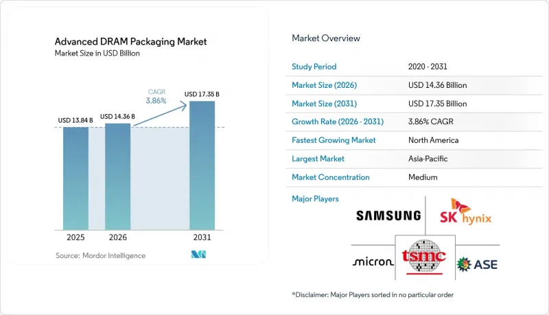
본 보고서는 패키징 유형(표준 DRAM 패키지, DRAM 기반 메모리용 패키지 온 패키지(PoP) 등), 집적 기술(와이어 본딩 등), 기판 유형(유기 기판 등), 생태계 채널(DRAM 제조업체, OSAT 등), 최종 용도(서버 및 데이터센터 등), 그리고 지역별로 분류되어 있습니다. 시장 전망은 금액(달러) 기준으로 제시되어 있습니다.
세계 첨단 DRAM 패키징 시장 동향 및 인사이트
AI 서버의 메모리 밀도 요구 사항 증가
AI 서버의 도입으로 인해 각 컴퓨팅 플랫폼은 이전 세대의 가속기보다 훨씬 더 많은 패키지 메모리를 탑재하게 되었습니다. 이러한 변화로 인해 첨단 DRAM 패키징 시장은 더 높은 적층 높이, 더 고밀도 상호 연결, 그리고 각 패키지 내부의 더 엄격한 열 제어에 대한 의존도를 높이고 있습니다. Samsung Electronics는 2026년 5월, 용량 48GB, 스택당 대역폭 3.6TB/s를 갖춘 12층 HBM4E 샘플을 출하했습니다. 이는 메모리 밀도와 대역폭이 동시에 향상되고 있음을 보여줍니다. 각 하이퍼스케일러 기업들이 맞춤형 가속기를 구축함에 따라, 첨단 DRAM 패키징 시장 전반에서 첨단 본딩 및 스태킹 공정을 지원할 수 있는 인증 고객 수도 확대되고 있습니다. 이로 인해 수요는 좁은 GPU 시장에 그치지 않고, 고밀도 패키징 프로그램을 지원할 수 있는 OSAT 및 수직 통합형 메모리 공급업체에 대해 보다 안정적인 수요가 창출되고 있습니다. 그 결과, 첨단 DRAM 패키징 시장에서는 서버 대수 증가뿐만 아니라 각 서버 플랫폼 내 메모리 탑재량 증가와 패키지 구조의 복잡화로 인해 수요가 확대되고 있습니다.
고대역폭 메모리 아키텍처로의 전환
HBM3E에서 HBM4로의 전환으로 인해, 첨단 DRAM 패키징 시장의 모든 인증 공급업체에게 기술적 장벽이 높아지고 있습니다. JEDEC는 2025년 4월, 2,048비트 인터페이스를 갖춘 HBM4 규격을 발표했습니다. 이로 인해 HBM3에 비해 대역폭이 2배로 증가하면서, 배선, 신호 무결성, 컨트롤러 설계에 걸친 패키징에 대한 요구 사항이 높아졌습니다. 이러한 요구 사항으로 인해 설계 채택은 실리콘 인터포저나 더 정교한 빌드업 기판으로 향하고 있습니다. 이는 기존의 유기 기판으로는 동등한 성능 수준에서 동등한 배선 부하를 감당할 수 없기 때문입니다. 또한, HBM4에서는 새로운 컨트롤러 접근 방식도 필요하기 때문에 확립된 공동 설계 관계를 갖춘 패키징 팀은 인증 주기에서 큰 우위를 점하게 될 것입니다. SK하이닉스는 2026년 초 청주 패키징 시설에 19조 원(128억 5,000만 달러 상당)을 투자할 것을 확정했습니다. 이는 첨단 DRAM 패키징 시장이 이러한 아키텍처 전환을 뒷받침하기 위해 얼마나 막대한 자본을 흡수하고 있는지를 여실히 보여줍니다. 이러한 전환은 패키지, 기판 선정, 컨트롤러, 그리고 공급업체 인증 프로세스를 동시에 변경하는 것이기 때문에 단순한 제품 개편이 아닙니다.
첨단 DRAM 패키징 라인의 높은 자본 집약도
자본 집약도는 최첨단 DRAM 패키징 시장이 어느 정도의 속도로 확대될 수 있는지에 있어 여전히 가장 명확한 제약 요인 중 하나입니다. SK하이닉스는 청주에 19조 원(128억 5,000만 달러)을 투자하는 최첨단 패키징 시설 건설을 추진한 데 이어, 인디애나주 프로젝트도 미국의 CHIPS 프로그램을 통해 직접적인 지원을 받고 있어, 현재 태평양 양안에서 매우 대규모의 자금 투입이 요구되고 있음을 보여줍니다. 마이크론 역시 최첨단 DRAM 제조, 연구개발(R&D), 그리고 선진적인 HBM 패키징 역량과 관련된 미국 내 투자 확대를 발표하며, 경쟁을 유지하기 위해 필요한 투자 규모가 얼마나 큰지를 뒷받침하고 있습니다. 최첨단 DRAM 패키징 시장은 고도의 본딩 기술, 웨이퍼 레벨 패키징, 그리고 테스트 장비의 조달 주기가 길고 클린룸에 대한 요구 사항도 까다로워 진입 장벽이 높은 상황입니다. 따라서 중소규모 OSAT(수탁 반도체 제조업체)나 모듈 조립업체는 정부의 지원이나 유력한 주요 고객을 확보하지 않는 한, 최상위 업체 반열에 진입하기 어렵습니다. 실질적인 영향으로 생산 능력 확충이 수요 동향보다 뒤처지고 있으며, 그 결과 최첨단 DRAM 패키징 시장 전체에서 공급 부족 상태가 지속되고 있습니다.
부문 분석
2025년, 표준 DRAM 패키지는 첨단 DRAM 패키지 시장 점유율의 49.67%를 차지하며 매출 기준 1위를 유지했습니다. 이러한 위상은 엔터프라이즈 서버, PC OEM 및 소비자용 기기에 널리 보급된 기존 DDR 시리즈 모듈의 방대한 도입 실적을 반영한 것입니다. 첨단 DRAM 패키징 시장에서는 전략적 관심이 HBM으로 이동하고 있지만, 출하량 측면에서는 여전히 이러한 표준 형식에 의존하고 있습니다. 패키지 온 패키지(PoP)는 콤팩트한 실적와 로직·메모리의 긴밀한 통합이 여전히 중요시되는 모바일 제품 분야에서 여전히 중요한 위치를 차지하고 있습니다.
3D 적층 DRAM과 함께 ‘기타’ 범주에 분류되는 HBM 패키지는 2031년까지 연평균 성장률(CAGR) 4.48%로 확대될 것으로 예측됩니다. 이러한 성장은 훨씬 더 높은 대역폭과 더 긴밀한 패키지 수준 통합을 필요로 하는 AI 가속기 및 맞춤형 ASIC 플랫폼에서 HBM의 활용이 확대되고 있음을 반영합니다. Samsung Electronics는 2026년 5월, 용량 48GB, 대역폭 3.6TB/s의 12층 HBM4E 샘플을 출하했습니다. 이는 첨단 DRAM 패키징 시장의 상위 부문이 더 고밀도이고 고속인 적층 구조로 전환되고 있음을 보여줍니다. 플립칩 DRAM 패키징은 HBM만큼의 비용이나 복잡성을 수반하지 않으면서도 전기적·열적 성능을 향상시키기 때문에 중요한 중간층으로서의 지위를 유지했습니다. 또한 WLCSP도 기판 공간이 제한된 저전력 IoT 및 엣지 디바이스에서 명확한 역할을 유지했습니다. 이에 따라 첨단 DRAM 패키징 업계는 대량 생산되는 범용 포맷과 생산량은 적지만 부가가치가 높은 HBM 구조로 양분되는 양상을 보였습니다. 이러한 양분화는 AI 시스템 도입이 진행됨에 따라 더욱 두드러질 가능성이 있습니다. 또한 이는 공급업체들이 HBM의 이익률 기회와 표준 DRAM 패키지의 규모의 경제 사이에서 균형을 맞추어야 함을 의미합니다.
2025년에는 와이어 본딩이 부문 매출의 47.45%를 차지하며, 규모 면에서 여전히 주요 집적 기술로서의 지위를 유지했습니다. 이 공정은 비트당 비용이 여전히 설계상의 최우선 과제인 표준 DRAM, 그래픽스 메모리 및 모바일 LPDDR 용도 분야에서 확고한 입지를 계속 유지하고 있습니다. 고성능 DRAM 패키지 시장에서도 대역폭이나 상호 연결 밀도 요구 사항이 그리 엄격하지 않은 카테고리에서는 이 기술을 대체하기가 여전히 어렵습니다. 따라서 플립 칩 본딩은 고성능 서버용 DRAM 모듈 및 그래픽스 메모리 분야에서 계속해서 안정적인 선택지로 자리매김했습니다.
TSV 기반 적층 기술은 2026년부터 2031년까지 4.52%라는 가장 높은 연평균 성장률(CAGR)을 나타낼 전망입니다. 이러한 성장은 AI 가속기 및 고성능 컴퓨팅(HPC) 플랫폼에서의 HBM 채택과 직접적으로 연결되어 있으며, 이러한 분야에서는 수직 적층이 성능의 핵심 요소입니다. 2,048비트 인터페이스를 포함한 HBM4의 기술 요구 사항은 TSV의 설계, 정렬 및 열 관리에 대한 부담을 가중시키고 있습니다. 다이 스태킹 및 웨이퍼 간 본딩은 특히 설계자들이 데이터 전송 및 패키지 통합에 대한 새로운 접근 방식을 모색하고 있는 분야에서 계속해서 보다 전문적인 역할을 수행하고 있습니다. 첨단 DRAM 패키징 시장은 특정 한 가지 기법이 완전히 주류가 되는 것이 아니라, 저비용과 고복잡성 양쪽의 통합 경로가 병행하여 유지될 가능성이 높다고 볼 수 있습니다. 이는 서버, 모바일 기기, 자동차 시스템, 소비자용 하드웨어 간에 용도 요구 사항이 여전히 크게 다르기 때문입니다. 따라서 기존 본딩과 차세대 TSV 워크플로우를 모두 지원할 수 있는 공급업체가 더 유리한 입장에 있습니다. 이러한 기술의 조합을 통해 볼 때, 첨단 DRAM 패키징 시장의 성장은 기존 조립 기법의 소멸에 기인한 것이 아니라 복잡성 증가에 기인한 것임을 알 수 있습니다.
지역별 분석
2025년, 아시아태평양은 첨단 DRAM 패키징 시장 점유율의 85.43%를 차지하며, 이 지역은 계속해서 지배적인 위치를 유지했습니다. 이러한 우위는 한국, 대만, 중국, 일본에 DRAM 제조, OSAT(위탁 반도체 조립) 생산 능력 및 기판 공급이 집중되어 있음을 반영한 것입니다. 특히 한국은 Samsung Electronics와 SK하이닉스가 전용 HBM 및 TSV 패키징 라인을 가동하는 한편, 새로운 메모리 및 패키징 시설에 대한 막대한 투자를 지속하고 있어 여전히 중요한 위치를 차지하고 있습니다. SK하이닉스는 2026년 초 청주 패키징 시설에 19조 원(128억 5,000만 달러) 규모의 투자를 확정하며, 고부가가치 메모리 패키징 분야에서 해당 지역의 리더십을 강화했습니다. 대만은 파운드리 연계형 패키징, 인터포저 공급 및 첨단 기판 생산이 깊이 뿌리내리고 있어 여전히 중요한 위치를 차지하고 있습니다.
북미는 2031년까지 연평균 성장률(CAGR) 4.67%를 나타낼 것으로 예측되며, 이는 첨단 DRAM 패키징 시장에서 가장 빠르게 확대되고 있는 지역 클러스터임을 보여줍니다. 미국의 정책 지원이 주요 요인으로 작용하고 있으며, 상무부는 2025년 1월, 시범 사업, 기판, 팬아웃 연구를 위해 14억 달러 규모의 첨단 패키징 보조금을 확정했습니다. SK하이닉스의 인디애나주 프로젝트도 CHIPS 프로그램의 지원을 받고 있으며, 미국 내 HBM 생산 및 메모리에 초점을 맞춘 연구 개발을 지원하기 위한 것입니다. 암코(Amcor)의 애리조나주 확장 사업은 북미가 설계 측면의 리더십에만 의존하지 않고, 현지 조립 체제를 심화시키고 있음을 다시 한번 보여줍니다.
유럽 및 기타 지역은 직접적인 매출 측면에서는 여전히 소규모에 그치고 있지만, 장비, 소재 및 선별적인 생산 능력 확장을 통해 첨단 DRAM 패키징 시장에 지속적으로 영향을 미치고 있습니다. 유럽의 역할은 업스트림 공정 인프라, 특히 HBM 프로그램에서 사용되는 첨단 DRAM 노드를 뒷받침하는 EUV 리소그래피 시스템과 밀접하게 연관되어 있습니다. 싱가포르 역시 메모리 패키징에 대한 새로운 투자를 통해 지역 내 반도체 거점으로서의 위상을 강화했습니다. 한편, 베트남은 보다 광범위한 패키징 체인에서 OSAT(위탁 반도체 조립)로서의 입지를 지속적으로 강화하고 있습니다. 이 지역들은 현재로서는 아시아태평양의 규모에는 미치지 못하지만, 첨단 DRAM 패키징 시장이 단일 지역의 효율성뿐만 아니라 공급망의 다양화와 현지화를 통해 점점 더 형성되고 있다는 점에서 중요한 의미를 지닙니다.
기타 혜택:
- 엑셀 형식 시장 예측(ME) 시트
- 3개월간의 애널리스트 지원
자주 묻는 질문
목차
제1장 서론
제2장 조사 방법
제3장 주요 요약
제4장 시장 구도
제5장 시장 규모와 성장 예측
제6장 경쟁 구도
제7장 시장 기회와 향후 전망
JHS 26.08.05According to Mordor Intelligence, the advanced DRAM packaging market size was USD 13.84 billion in 2025, USD 14.36 billion and is forecast to reach USD 17.35 billion by 2031 at a CAGR of 3.86% over 2026-2031.
This report is Segmented by Packaging Type (Standard DRAM Packaging, Package-On-Package (PoP) for DRAM-Based Memory, and More), Integration Technology (Wire Bonding, and More), Substrate Type (Organic Substrate, and More), Ecosystem Channel (DRAM Manufacturers, Osats, and More) End Use (Servers and Data Centers, and More), and Geography. The Market Forecasts are Provided in Terms of Value (USD).
Global Advanced DRAM Packaging Market Trends and Insights
Rising AI Server Memory Density Requirements
AI server deployment is pushing each compute platform to carry much more packaged memory than earlier accelerator generations. That shift is making the advanced DRAM packaging market more dependent on higher stack heights, denser interconnects, and stricter thermal control inside each package. Samsung shipped 12-layer HBM4E samples with 48GB capacity and 3.6TB/s per-stack bandwidth in May 2026, which shows how memory density and bandwidth are moving higher at the same time. As more hyperscalers build custom accelerators, the number of qualified customers for advanced bonding and stacking flows is also widening across the advanced DRAM packaging market. That broadens volume demand beyond a narrow GPU base and creates steadier pull for OSATs and vertically integrated memory suppliers that can support high-density packaging programs. The result is that the advanced DRAM packaging market is seeing demand growth not just from more servers, but from more memory content and more complex package structures inside each server platform.
Transition To Higher Bandwidth Memory Architectures
The move from HBM3E to HBM4 is raising the technical threshold for every qualified supplier in the advanced DRAM packaging market. JEDEC published the HBM4 standard in April 2025 with a 2,048-bit interface, which doubled the width from HBM3 and lifted packaging demands across routing, signal integrity, and controller design.Those requirements are steering design wins toward silicon interposers and more advanced build-up substrates because conventional organic formats cannot manage the same routing burden at similar performance levels. HBM4 also requires a new controller approach, so packaging teams with established co-design relationships gain a meaningful lead in qualification cycles. SK hynix confirmed a KRW 19 trillion investment, equivalent to USD 12.85 billion, for its packaging facility in Cheongju in early 2026, which underlines how the advanced DRAM packaging market is absorbing capital to support this architecture shift. This migration is not a simple product refresh, because it changes the package, the substrate choice, the controller, and the supplier qualification path at the same time.
High Capital Intensity of Advanced DRAM Packaging Lines
Capital intensity remains one of the clearest limits on how quickly the advanced DRAM packaging market can expand. SK hynix moved ahead with a KRW 19 trillion, or USD 12.85 billion, advanced packaging facility in Cheongju, while its Indiana project also received direct support through the U.S. CHIPS program, showing that very large funding commitments are now required on both sides of the Pacific. Micron also announced expanded U.S. investments tied to leading-edge DRAM manufacturing, R&D, and advanced HBM packaging capability, reinforcing the scale of spending needed to stay competitive. The advanced DRAM packaging market faces a high entry barrier because advanced bonding, wafer-level packaging, and test equipment come with long procurement cycles and large cleanroom requirements. That keeps smaller OSATs and module assemblers from entering the top tier unless they secure government support or a strong anchor customer. The practical effect is that capacity additions are slower than demand signals, which preserves supply tightness across the advanced DRAM packaging market.
Other drivers and restraints analyzed in the detailed report include:
- Heterogeneous Integration Demand in Advanced Nodes
- Expanding Outsourced Advanced Packaging Capacity
- Yield Loss Risk In Multi-Die And TSV-Based Stacking
For complete list of drivers and restraints, kindly check the Table Of Contents.
Segment Analysis
Standard DRAM packaging held 49.67% of the advanced DRAM packaging market share in 2025, which kept it in the leading position by revenue. This position reflected the large installed base of conventional DDR-series modules across enterprise servers, PC original equipment manufacturers, and consumer devices. The advanced DRAM packaging market still relies on these standard formats for shipment volume even while strategic attention has moved toward HBM. Package-on-Package remained relevant in mobile products where a compact footprint and close logic-memory integration still matter.
HBM packaging, grouped within the Others category alongside 3D stacked DRAM, is projected to expand at a 4.48% CAGR through 2031. That growth reflects the widening use of HBM across AI accelerators and custom ASIC platforms that need much higher bandwidth and tighter package-level integration. Samsung shipped 12-layer HBM4E samples in May 2026 with 48GB capacity and 3.6TB/s bandwidth, which showed how the high end of the advanced DRAM packaging market is moving toward denser and faster stacks. Flip-chip DRAM packaging remained an important middle tier because it improves electrical and thermal performance without reaching the full cost and complexity of HBM. WLCSP also kept a clear role in low-power IoT and edge devices where board space is limited. This leaves the advanced DRAM packaging industry split between high-volume commodity formats and lower-volume, higher-value HBM structures. That split is likely to become more pronounced as AI system procurement continues. It also means suppliers must balance margin opportunities in HBM against the scale advantages of standard DRAM packages.
Wire bonding accounted for 47.45% of segment revenue in 2025, which kept it as the leading integration technology by scale. The process stayed entrenched in standard DRAM, graphics memory, and mobile LPDDR applications where cost-per-bit is still the main design priority. In the advanced DRAM packaging market, this technology remains hard to displace in categories where bandwidth and interconnect density requirements are less demanding. Flip-chip bonding therefore continued as a stable option for higher-performance server DRAM modules and graphics memory.
TSV-based stacking is projected to register the fastest CAGR of 4.52% over 2026-2031. Its growth is tied directly to HBM adoption in AI accelerators and high-performance computing platforms, where vertical stacking is central to performance. HBM4 technical requirements, including a 2,048-bit interface, are increasing the burden on TSV design, alignment, and thermal control. Die stacking and wafer-to-wafer bonding continue to serve more specialized roles, especially where designers are testing newer approaches to data movement and package integration. The advanced DRAM packaging market is likely to keep both low-cost and high-complexity integration paths in parallel rather than move fully to one dominant method. That is because application needs remain very different across servers, mobile devices, automotive systems, and consumer hardware. Suppliers that can support both legacy bonding and next-generation TSV workflows are therefore in a stronger position. The technology mix also shows that growth in the advanced DRAM packaging market is coming from complexity, not from the disappearance of older assembly methods.
Complete Report Scope:
- By Packaging Type
- Standard DRAM Packaging
- Package-on-Package (PoP) for DRAM-Based Memory Modules
- Flip-Chip DRAM Packaging
- Wafer-Level Chip Scale Packaging (WLCSP)
- Other Packaging Types (3D Stacked DRAM Packaging, High Bandwidth Memory (HBM) Packaging)
- By Integration Technology
- Wire Bonding
- Flip-Chip Bonding
- Through-Silicon Via (TSV) Based Stacking
- Die Stacking
- Wafer-to-Wafer Bonding
- Other Integration Technologies (Die-to-Wafer Bonding, Hybrid Bonding)
- By Substrate / Interposer Type
- Organic Substrate
- Leadframe Package
- Silicon Interposer / TSV-Based Interconnect
- Advanced Build-Up Substrate
- Other Substrate / Interposer Types (Fan-Out Wafer-Level Packaging, Emerging Advanced Substrates)
- By Ecosystem Channel
- DRAM Manufacturers
- OSATs
- Advanced Packaging Foundries
- Module Assemblers
- By End Use
- Servers and Data Centers
- PCs and Laptops
- Smartphones and Tablets
- Consumer Electronics
- Other End Uses (Graphics and Gaming Devices, Automotive Electronics)
- By Geography
- North America
- Europe
- Asia-Pacific
- China
- Japan
- South Korea
- Taiwan
- Rest of Asia-Pacific
- Rest of the World
Geography Analysis
Asia-Pacific held 85.43% of the advanced DRAM packaging market share in 2025, which kept the region in a dominant position. This lead reflected the concentration of DRAM fabrication, OSAT capacity, and substrate supply across South Korea, Taiwan, China, and Japan. South Korea remained especially important because Samsung Electronics and SK hynix operate dedicated HBM and TSV packaging lines while continuing to invest heavily in new memory and packaging facilities. SK hynix confirmed a KRW 19 trillion investment, (USD 12.85 billion), for its Cheongju packaging facility in early 2026, reinforcing the region's leadership in high-value memory packaging. Taiwan remained critical because foundry-linked packaging, interposer supply, and advanced substrate production are deeply embedded there.
North America is projected to grow at a 4.67% CAGR through 2031, which makes it the fastest-expanding regional cluster in the advanced DRAM packaging market. U.S. policy support is a major factor, with the Department of Commerce finalizing USD 1.4 billion in advanced packaging awards in January 2025 for piloting, substrates, and fan-out research. SK hynix's Indiana project also received CHIPS program backing and is intended to support HBM production and memory-focused R&D in the United States. Amkor's Arizona expansion further shows that North America is building local assembly depth rather than relying only on design leadership.
Europe and the rest of the world remained smaller in direct revenue terms, but they still influenced the advanced DRAM packaging market through equipment, materials, and selective capacity additions. Europe's role is tied to upstream process infrastructure, especially EUV lithography systems that support the advanced DRAM nodes used in HBM programs. Singapore also strengthened its position as a regional semiconductor base through new memory packaging investment, while Vietnam continued to build out OSAT relevance in the broader packaging chain. These areas do not challenge Asia-Pacific's scale today, but they matter because the advanced DRAM packaging market is increasingly shaped by supply chain diversification and localization rather than by one-region efficiency alone.
- Samsung Electronics Co., Ltd.
- SK hynix Inc.
- Micron Technology, Inc.
- Taiwan Semiconductor Manufacturing Company Limited
- Advanced Semiconductor Engineering, Inc.
- Amkor Technology, Inc.
- Powertech Technology Inc.
- Jiangsu Changjiang Electronics Technology Co., Ltd.
- King Yuan Electronics Co., Ltd.
- Siliconware Precision Industries Co., Ltd.
- TongFu Microelectronics Co., Ltd.
- Hana Micron Inc.
- ChipMOS TECHNOLOGIES INC.
- Tianshui Huatian Technology Co., Ltd.
- Fujitsu Limited
- Intel Corporation
- Kioxia Corporation
- Tokyo Electron Limited
- United Microelectronics Corporation
- JCET Group Co., Ltd.
Additional Benefits:
- The market estimate (ME) sheet in Excel format
- 3 months of analyst support
TABLE OF CONTENTS
1 INTRODUCTION
- 1.1 Study Assumptions and Market Definition
- 1.2 Scope of the Study
2 RESEARCH METHODOLOGY
3 EXECUTIVE SUMMARY
4 MARKET LANDSCAPE
- 4.1 Market Overview
- 4.2 Impact of Macroeconomic Factors on the Market
- 4.3 Market Drivers
- 4.3.1 Rising AI Server Memory Density Requirements
- 4.3.2 Transition to Higher Bandwidth Memory Architectures
- 4.3.3 Heterogeneous Integration Demand in Advanced Nodes
- 4.3.4 Expanding Outsourced Advanced Packaging Capacity
- 4.3.5 Thermal and Signal Integrity Constraints in High-Performance DRAM
- 4.3.6 Government Incentives for Semiconductor Supply Chain Localization
- 4.4 Market Restraints
- 4.4.1 High Capital Intensity of Advanced DRAM Packaging Lines
- 4.4.2 Yield Loss Risk in Multi-Die and TSV-Based Stacking
- 4.4.3 Limited Substrate and Interposer Supply in Peak Cycles
- 4.4.4 Qualification Complexity for Memory-Logic Co-Design Flows
- 4.5 Industry Supply Chain Analysis
- 4.6 Regulatory Landscape
- 4.7 Technological Outlook
- 4.8 Porter's Five Forces Analysis
- 4.8.1 Bargaining Power of Suppliers
- 4.8.2 Bargaining Power of Buyers
- 4.8.3 Threat of New Entrants
- 4.8.4 Threat of Substitutes
- 4.8.5 Intensity of Competitive Rivalry
5 MARKET SIZE AND GROWTH FORECASTS (VALUE)
- 5.1 By Packaging Type
- 5.1.1 Standard DRAM Packaging
- 5.1.2 Package-on-Package (PoP) for DRAM-Based Memory Modules
- 5.1.3 Flip-Chip DRAM Packaging
- 5.1.4 Wafer-Level Chip Scale Packaging (WLCSP)
- 5.1.5 Other Packaging Types (3D Stacked DRAM Packaging, High Bandwidth Memory (HBM) Packaging)
- 5.2 By Integration Technology
- 5.2.1 Wire Bonding
- 5.2.2 Flip-Chip Bonding
- 5.2.3 Through-Silicon Via (TSV) Based Stacking
- 5.2.4 Die Stacking
- 5.2.5 Wafer-to-Wafer Bonding
- 5.2.6 Other Integration Technologies (Die-to-Wafer Bonding, Hybrid Bonding)
- 5.3 By Substrate / Interposer Type
- 5.3.1 Organic Substrate
- 5.3.2 Leadframe Package
- 5.3.3 Silicon Interposer / TSV-Based Interconnect
- 5.3.4 Advanced Build-Up Substrate
- 5.3.5 Other Substrate / Interposer Types (Fan-Out Wafer-Level Packaging, Emerging Advanced Substrates)
- 5.4 By Ecosystem Channel
- 5.4.1 DRAM Manufacturers
- 5.4.2 OSATs
- 5.4.3 Advanced Packaging Foundries
- 5.4.4 Module Assemblers
- 5.5 By End Use
- 5.5.1 Servers and Data Centers
- 5.5.2 PCs and Laptops
- 5.5.3 Smartphones and Tablets
- 5.5.4 Consumer Electronics
- 5.5.5 Other End Uses (Graphics and Gaming Devices, Automotive Electronics)
- 5.6 By Geography
- 5.6.1 North America
- 5.6.2 Europe
- 5.6.3 Asia-Pacific
- 5.6.3.1 China
- 5.6.3.2 Japan
- 5.6.3.3 South Korea
- 5.6.3.4 Taiwan
- 5.6.3.5 Rest of Asia-Pacific
- 5.6.4 Rest of the World
6 COMPETITIVE LANDSCAPE
- 6.1 Market Concentration
- 6.2 Strategic Moves
- 6.3 Market Share Analysis
- 6.4 Company Profiles (includes Global Level Overview, Market Level Overview, Core Segments, Financials as available, Strategic Information, Market Rank/Share, Products and Services, Recent Developments)
- 6.4.1 Samsung Electronics Co., Ltd.
- 6.4.2 SK hynix Inc.
- 6.4.3 Micron Technology, Inc.
- 6.4.4 Taiwan Semiconductor Manufacturing Company Limited
- 6.4.5 Advanced Semiconductor Engineering, Inc.
- 6.4.6 Amkor Technology, Inc.
- 6.4.7 Powertech Technology Inc.
- 6.4.8 Jiangsu Changjiang Electronics Technology Co., Ltd.
- 6.4.9 King Yuan Electronics Co., Ltd.
- 6.4.10 Siliconware Precision Industries Co., Ltd.
- 6.4.11 TongFu Microelectronics Co., Ltd.
- 6.4.12 Hana Micron Inc.
- 6.4.13 ChipMOS TECHNOLOGIES INC.
- 6.4.14 Tianshui Huatian Technology Co., Ltd.
- 6.4.15 Fujitsu Limited
- 6.4.16 Intel Corporation
- 6.4.17 Kioxia Corporation
- 6.4.18 Tokyo Electron Limited
- 6.4.19 United Microelectronics Corporation
- 6.4.20 JCET Group Co., Ltd.
7 MARKET OPPORTUNITIES AND FUTURE OUTLOOK
- 7.1 White-Space and Unmet-Need Assessment


