

|
시장보고서
상품코드
2099447
HBM 제조 장비 : 시장 점유율 분석, 업계 동향 및 통계, 성장 예측(2026-2031년)HBM Manufacturing Equipment - Market Share Analysis, Industry Trends & Statistics, Growth Forecasts (2026 - 2031) |
||||||
 Mordor Intelligence
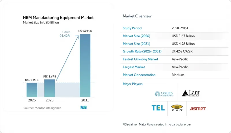
Mordor Intelligence에 의하면, HBM 제조 장비 시장 규모는 2025년 12억 8,000만 달러로 평가되었습니다. 2026년에는 16억 7,000만 달러로 확대되어 2031년까지 49억 8,000만 달러에 이를 것으로 예상되고 2026년부터 2031년에 걸쳐 CAGR 24.40%로 성장할 전망입니다.
본 보고서는 장비 유형(TSV 에칭 장비 등), 본딩 기술(열압축 본딩, 하이브리드 본딩 등), HBM 세대(HBM2E, HBM3, HBM3E 등), 적층 방식(다이-투-웨이퍼, 웨이퍼-투-웨이퍼, 다이-투-다이), 최종 사용자(메모리 제조업체, 파운드리, OSAT), 지역별로 분류되어 있습니다. 시장 전망은 금액(달러) 기준으로 제시되어 있습니다.
세계의 HBM 제조 장비 시장 동향 및 인사이트
AI 메모리의 적층 밀도가 TSV 및 하이브리드 본딩 장비 수요를 견인
HBM 제조 장비 시장은 현재, 기존 DRAM의 교체 주기보다 AI 가속기의 도입과 더 밀접하게 연계되어 있습니다. AI 모델의 복잡성이 증가함에 따라 메모리 스택은 더 고밀도의 TSV 어레이, 더 좁은 본딩 피치, 그리고 더 정교한 평탄화 공정으로 진화하고 있으며, 이로 인해 웨이퍼 1장당 장비 사용량이 증가하고 있습니다. 애플라이드 머티리얼즈(Applied Materials)는 초미세 피치 노드에서 TSV 어레이 전체의 도금 불균일성을 해결하기 위해, 적응형 패턴 조정 기능을 갖춘 전기화학 도금 장비 ‘Nokota Vmax 2’를 발표했습니다. 이것이 중요한 이유는 이전 미세화 단계에서는 허용 범위 내였던 결함이 현재는 멀티다이 스택 전체의 수율을 저하시킬 가능성이 있기 때문입니다. 따라서 HBM 제조 장비 시장에서는 컴퓨팅 로드맵에 따른 수요가 나타나고 있습니다. NVIDIA의 Rubin 플랫폼 사양(HBM4 스택 8층, 총 대역폭 22테라바이트/초)이 이미 공급업체의 계획에 영향을 미치고 있기 때문입니다. 이러한 요인들이 복합적으로 작용하여, 예측 기간 동안 장비 수요는 명확하고 지속적일 것으로 보입니다.
HBM4 및 저피치 상호 연결로의 전환
HBM4는 2,048비트 인터페이스로의 전환과 스택당 대역폭을 초당 2테라바이트 이상으로 끌어올림으로써, HBM 제조 장비 시장의 기술적 장벽을 한층 더 높이고 있습니다. 이러한 변화에 대응하기 위해서는 두께 약 30마이크로미터의 개별 DRAM 다이를 처리하면서, 스택 전체에 걸쳐 100나노미터 미만의 공차 내에서 정렬을 유지할 수 있는 장비가 필요합니다. Besi사는 2026년 1분기 설명회에서 주요 메모리 제조업체 3곳 모두 동일한 고객 요구 사항에 따라 하이브리드 본딩 장비를 평가 중이며, 하이브리드 본딩된 스택의 상용화는 2027년을 목표로 하고 있다고 밝혔습니다. 또한, HBM4의 베이스 다이가 기존의 메모리 제조 공정에만 국한되지 않고 TSMC의 첨단 로직 노드에서 제조되게 됨에 따라 대만 내 수요도 확대되고 있습니다. 이에 따라 본딩, CMP, 계측, TSV 각 공정이 메모리와 파운드리 양쪽의 인증 기준을 모두 충족해야 할 필요가 생겨 장비 구성도 변화하고 있습니다. 따라서 HBM 제조 장비 시장은 스택 수 증가뿐만 아니라, 로직 집적도가 높은 베이스 다이를 지원하기 위해 필요한 보다 광범위한 공정 통합을 통해 재편되고 있습니다.
매우 높은 설비 투자 강도와 긴 인증 주기
HBM 제조 장비 시장의 큰 제약 요인은 차세대 본딩 시스템의 높은 비용과, 해당 장비가 생산 수율을 뒷받침할 수 있게 되기까지 필요한 긴 인증 주기입니다. 이러한 비용 구조로 인해, 디바이스 수요가 왕성할 때에도 장비 선정은 고객의 팹 내 긴 검증 기간과 조화를 이루어야 하므로 조달이 지연됩니다. 또한, 이러한 부담은 고르지 않습니다. 왜냐하면 확립된 공정 제휴 관계를 맺고 있는 대형 메모리 제조업체는 패키징 분야에 신규로 진입한 기업이나 OSAT(수탁 조립 업체)보다 신속하게 대응할 수 있기 때문입니다. 경우에 따라서는 신규 진출기업이 생산 라인을 가동 가능한 상태로 만드는 데 18개월이 넘는 인증 기간이 소요되기도 합니다. 따라서 설비 투자 억제나 인증 리스크로 인해 고객층이 좁아지기 때문에 HBM 제조 장비 시장의 성장은 최종 수요만으로 예상되는 것보다 완만해지고 있습니다.
부문 분석
2025년, 웨이퍼/다이 본딩 장비는 HBM 제조 장비 시장 점유율의 33.81%를 차지하며, 현행 생산 라인에서 가장 큰 장비 카테고리가 되었습니다. 이러한 우위는 SK하이닉스, 삼성, 마이크론의 HBM3E 양산에 기인하며, 이들 기업에서는 다이 스태킹의 핵심 장비로서 여전히 열압축 본더가 사용되고 있습니다. 이러한 지위는 긴 인증 주기에도 힘입고 있습니다. 완전히 승인된 본딩 장비는 일단 대량 생산 라인에 도입되면 교체가 어렵기 때문입니다. TSV 에칭 장비 및 CMP 장비는 에칭이 비아 구조를 형성하고, CMP가 후속 본딩 공정을 위한 표면 처리를 수행하기 때문에 중요한 관련 공정 분야로서 그 뒤를 잇고 있습니다. HBM 제조 장비 시장에서는 이러한 밀접하게 연계된 공정에서 처리량과 재현성을 모두 지원할 수 있는 공급업체가 계속해서 우위를 점하고 있습니다.
임시 본딩 및 디본딩 장비는 DRAM 다이의 박형화 및 스택 설계의 고층화로의 전환을 반영하여, 2026년부터 2031년에 걸쳐 연평균 성장률(CAGR) 25.38%로 가장 빠르게 성장할 것으로 예측됩니다. EV Group사는 자사의 IR Layer Release 기술을 통해 실리콘의 나노미터 수준 정밀도로 레이저 디본딩이 가능해져, 첨단 임시 본딩 공정에서 유리 기판이 더 이상 필요하지 않게 될 것이라고 밝혔습니다. 이는 스택 수가 증가하고 웨이퍼의 박형화가 진행됨에 따라 30마이크로미터 미만의 다이를 취급하기가 더욱 어려워지기 때문에 중요한 의미를 지닙니다. SUSS MicroTec사는 임시 본딩 및 디본딩 분야에서 확고한 입지를 유지하고 있으며, 이는 현재의 HBM 양산 확대와 미래의 웨이퍼 레벨 스태킹 프로그램 모두에서 중요한 역할을 하고 있습니다. 고객들이 복잡한 패키징 공정 전반에 걸친 통합 시간을 단축하고자 하는 가운데, 이러한 장비군 간의 상호 운용성은 점점 더 중요해지고 있습니다. 따라서 HBM 제조 장비 업계에서는 새로운 공정의 마찰을 일으키지 않고 기존 라인에 통합할 수 있는 공급업체를 높이 평가했습니다. 결과적으로 HBM 제조 장비 시장은 장비 대수 증가뿐만 아니라 호환 가능한 다단계 플랫폼에 대한 수요 증가에 힘입어 확대되고 있습니다.
2025년에는 HBM 제조 장비 시장의 72.46%를 열압축 본딩이 차지했으며, 이는 HBM3E 생산에서 거의 보편적으로 채택되고 있음을 반영합니다. 알려진 열 및 압력 제어 프로파일을 사용하여 9-55 마이크로미터 피치의 적층 DRAM 어셈블리를 처리할 수 있기 때문에 여전히 생산의 표준으로 자리 잡고 있습니다. 이는 HBM 제조 장비 시장에서 단일 고객에 대한 의존도가 여전히 주요 본딩 공급업체의 경제성을 좌우할 수 있음을 보여줍니다. 또한, 일시적인 웨이퍼 본딩 및 디본딩도 열압축 라인과 병행하여 성장하고 있습니다. 이는 연마, TSV 노광, 메탈라이제이션 각 공정에서 보다 안전한 취급을 실현하기 위함입니다.
하이브리드 본딩은 2026년부터 2031년까지 연평균 성장률(CAGR) 25.89%를 나타낼 것으로 예측되며, 스택 높이가 현재 열압축 기술의 한계를 넘어섬에 따라 가장 빠르게 성장하는 본딩 기술이 될 전망입니다. SUSS MicroTec사는 웨이퍼 간 본딩, 일괄 다이-웨이퍼 간 본딩, 순차적 다이-웨이퍼 간 본딩을 아우르는 통합 시스템으로 XBC300 Gen2D2W 플랫폼을 발표했습니다. 이 플랫폼은 ±100나노미터의 정렬 정밀도를 실현하고 있습니다. 삼성은 SEMES를 통해 사내에서 하이브리드 본딩을 개발하고 있는 반면, Besi는 이미 주요 메모리 제조업체 3곳 모두에 평가용 장비를 출하했습니다. 이러한 전환은 중요한 의미를 지닙니다. 제로 갭 구리 대 구리 본딩은 범프 기반 상호 연결보다 단위 면적당 대역폭 밀도를 높일 수 있기 때문입니다. 다만, 하이브리드 본딩의 비용은 다이당 플립칩 본딩의 2-3배이며, 수율 향상을 통해 비용을 절감해야 하므로 도입은 여전히 단계적으로 진행될 것입니다. 따라서 HBM 제조 장비 업계는 기존 방식과 차세대 본딩 라인이 공존하는 시기에 접어들었습니다. 이러한 공존으로 인해 현재의 양산에 대응하면서도 미래의 인증 획득도 확보할 수 있는 벤더에게 HBM 제조 장비 시장은 계속해서 매력적인 시장으로 남아 있습니다.
지역별 분석
아시아태평양은 2025년 HBM 제조 장비 시장 규모의 82.14%를 차지했으며, 2031년까지 연평균 성장률(CAGR) 25.28%를 나타낼 것으로 예측됩니다. 한국은 최대 규모의 HBM 생산 거점을 보유하고 있을 뿐만 아니라, 패키징 및 파브리케이션 분야에서의 주요 신규 투자도 추진하고 있어 이 지역에서 중심적인 위치를 유지하고 있습니다. 대만은 TSMC의 첨단 파운드리 서비스 덕분에 HBM 베이스 다이 생산이 로직 집적도가 높은 제조 라인으로 전환되고 있어 그 중요성이 점점 더 커지고 있습니다. 일본 또한 SCREEN, DISCO, ULVAC, 도쿄 일렉트론과 같은 국내 장비 공급업체를 통해, 그리고 히로시마에서 마이크론의 HBM 사업 확장을 통해 이중적인 역할을 수행하고 있습니다. HBM 제조 장비 시장이 아시아태평양에 계속 집중되고 있는 것은 해당 지역이 메모리 생산, 공급업체의 밀집도, 그리고 확립된 인증 인프라를 모두 갖추고 있기 때문입니다. 중국은 여전히 독자적인 국내 생태계 구축을 추진하고 있지만, 첨단 패키징 장비에 대한 수출 규제로 인해 세계 최고 수준의 장비에 대한 접근은 계속해서 제한되고 있습니다. 그 결과, 주요 지역 수요 거점의 기존 공급업체에 대한 직접적인 도전이라기보다는 현지에서의 장비 개발이라는 병행 경로가 생겨나고 있습니다.
현재 HBM 제조 장비 시장에서 북미의 점유율은 여전히 아시아태평양에 비해 훨씬 작지만, 미국의 반도체 인센티브가 신규 생산 능력 확대를 뒷받침하고 있어 그 장기적인 역할은 강화되고 있습니다. 마이크론(Micron)이 뉴욕주 오논다가 카운티에 대규모 제조 거점을 건설할 계획인 데다, 보이시(Boise)에서의 확장도 진행되고 있어, 미국은 본딩, TSV 및 첨단 패키징 장비 분야에서 더욱 중요한 미래 수요 거점으로 변모하고 있습니다. 유럽은 메모리 생산에 대한 기여도는 낮지만, 공급업체의 강점, 특히 오스트리아의 EV Group과 독일의 SUSS MicroTec을 통해 큰 역할을 수행하고 있습니다. EV Group은 웨이퍼 본딩 및 층간 전사 분야에서 여전히 중심적인 위치를 차지하고 있는 반면, SUSS MicroTec은 HBM 제조 장비 시장의 다음 단계에 대응하는 하이브리드 본딩 기술 개발을 추진하고 있습니다. 네덜란드의 Besi 역시 주요 메모리 제조업체 3곳 모두가 이 회사의 하이브리드 본딩 장비를 높이 평가하고 있어 전략적으로 중요한 위치를 차지하고 있습니다.
남미, 중동 및 아프리카는 현재 HBM 제조 장비 시장 수요에서 극히 미미한 점유율만을 차지하고 있습니다. 두 지역 모두 HBM 제조나 첨단 패키징의 주요 도입 실적이 없기 때문에 장비에 대한 투자는 소규모 테스트나 전자기기 조립 수요로 제한되어 있습니다. 일부 걸프 지역의 정부 반도체 프로그램이나 브라질의 전자기기 장려 제도는 장기적인 패키징 활동을 뒷받침할 가능성이 있지만, HBM에 특화된 실질적인 조달은 현재 예측 기간 내에는 예상되지 않습니다. 그러나 HBM 제조 장비 시장은 지리적으로 집중되어 있으며, 주요 경쟁 및 투자 동향은 여전히 아시아태평양을 중심으로 북미 및 유럽의 특정 프로젝트로 한정되어 있습니다.
기타 혜택 :
- 엑셀 형식 시장 예측(ME) 시트
- 3개월간의 애널리스트 지원
자주 묻는 질문
목차
제1장 서론
제2장 조사 방법
제3장 주요 요약
제4장 시장 구도
제5장 시장 규모 및 성장 예측
제6장 경쟁 구도
제7장 시장 기회 및 향후 전망
KTH 26.08.10According to Mordor Intelligence, the HBM manufacturing equipment market size is expected to increase from USD 1.28 billion in 2025 to USD 1.67 billion in 2026 and reach USD 4.98 billion by 2031, growing at a CAGR of 24.40% over 2026-2031.
This report is Segmented by Equipment Type (TSV Etch Equipment, and More), Bonding Technology (Thermocompression Bonding, Hybrid Bonding, and More), HBM Generation (HBM2E, HBM3, HBM3E, and More), Stacking Method (Die-To-Wafer, Wafer-To-Wafer, and Die-To-Die), End User (Memory Makers, Foundries, and OSATs), and Geography. The Market Forecasts are Provided in Terms of Value (USD).
Global HBM Manufacturing Equipment Market Trends and Insights
AI Memory Stack Density Driving TSV And Hybrid Bonding Tool Demand
The HBM manufacturing equipment market is now tied more closely to AI accelerator deployment than to the older DRAM replacement cycle. Higher AI model complexity is pushing memory stacks toward denser TSV arrays, tighter bonding pitch, and more demanding planarization steps, which raises equipment intensity per wafer start. Applied Materials introduced the Nokota Vmax 2 electrochemical deposition tool with adaptive pattern tuning to address plating variation across TSV arrays at very fine pitch nodes. This matters because defects that were manageable at earlier geometries can now reduce yield across an entire multi-die stack. The HBM manufacturing equipment market is therefore seeing demand that follows compute roadmaps, as NVIDIA's Rubin platform specification for 8 HBM4 stacks and 22 terabytes per second of aggregate bandwidth is already influencing supplier planning. That combination makes tool demand both visible and durable through the forecast period.
Migration To HBM4 And Lower-Pitch Interconnects
HBM4 is raising the technical bar for the HBM manufacturing equipment market by moving to a 2,048-bit interface and pushing per-stack bandwidth above 2 terabytes per second. Those changes require tools that can handle individual DRAM dies measuring nearly 30 micrometers thick while maintaining alignment within sub-100-nanometer tolerances across the full stack. Besi stated in its Q1 2026 discussion that all 3 major memory manufacturers are evaluating hybrid bonding tools to the same customer requirement, with commercial deployment of hybrid-bonded stacks targeted for 2027. The transition is also expanding demand in Taiwan, as HBM4 base dies are being fabricated on advanced logic nodes at TSMC rather than remaining entirely within traditional memory flows. That changes the tool mix, since bonding, CMP, metrology, and TSV steps now need to satisfy both memory and foundry qualification standards. The HBM manufacturing equipment market is therefore being reshaped not only by higher stack counts, but also by the broader process integration required to support logic-rich base dies.
Extreme Capex Intensity And Long Qualification Cycles
A major limit on the HBM manufacturing equipment market is the high cost of next-generation bonding systems and the long qualification cycle needed before those tools can support production yield. That cost structure slows procurement even when device demand is strong, because tool decisions must be matched with long validation periods inside customer fabs. The burden is also uneven, since large memory makers with established process relationships can move faster than new packaging entrants or OSATs. In some cases, new participants may face qualification timelines of more than 18 months before a line becomes production-ready. The HBM manufacturing equipment market, therefore, grows more slowly than end demand alone would suggest, because capex discipline and qualification risk narrow the customer set.
Other drivers and restraints analyzed in the detailed report include:
- Advanced Packaging Capacity Additions By Memory Makers
- Rising Need For Ultra-Flat Surfaces And Defect-Free Interfaces
- Yield Sensitivity In High-Aspect-Ratio Tsv And Hybrid Bonding Flows
For complete list of drivers and restraints, kindly check the Table Of Contents.
Segment Analysis
Wafer/Die Bonding Equipment held 33.81% of the HBM manufacturing equipment market share in 2025, which made it the largest equipment category in current production lines. Its lead came from HBM3E volume manufacturing across SK hynix, Samsung, and Micron, where thermocompression bonders remain the central tool for die stacking. This position is also supported by long qualification cycles, because a fully approved bonding tool is difficult to displace once it is embedded in a high-volume line. TSV Etch Equipment and CMP Equipment followed as important linked process categories, since etch forms the via structure and CMP prepares the surface for later bonding stages. The HBM manufacturing equipment market continues to reward vendors that can support both throughput and repeatability in these tightly linked steps.
Temporary Bonding and Debonding Equipment is projected to grow the fastest, at a 25.38% CAGR from 2026 to 2031, reflecting the move toward thinner DRAM dies and taller stack designs. EV Group said its IR Layer Release technology enables nanometer-level precision laser debonding of silicon and eliminates the need for glass substrates in advanced temporary bonding flows. That matters because handling dies below 30 micrometers becomes more difficult as stack counts rise and wafer thinning intensifies. SUSS MicroTec has maintained a strong position in temporary bonding and debonding, which makes it relevant to both today's HBM ramps and future wafer-level stacking programs. Interoperability across these tool sets is becoming more important as customers try to reduce integration time across complex packaging flows. That is why the HBM manufacturing equipment industry is placing greater value on suppliers that can fit into an existing line without creating new process friction. The HBM manufacturing equipment market is therefore expanding not only through higher tool counts, but also through the growing need for compatible multi-step platforms.
Thermocompression bonding accounted for 72.46% of the HBM manufacturing equipment market in 2025, reflecting its near-universal use across HBM3E production. It remains the production standard because it can support stacked DRAM assembly at pitches of 9 to 55 micrometers with known heat and pressure control profiles. This shows how single-customer exposure can still define the economics of a major bonding supplier in the HBM manufacturing equipment market. Temporary wafer bonding and debonding also grow alongside thermocompression lines because it enables safer handling during grinding, TSV exposure, and metallization.
Hybrid bonding is projected to grow at a 25.89% CAGR from 2026 to 2031, making it the fastest-growing bonding technology as stack heights exceed current thermocompression limits. SUSS MicroTec introduced the XBC300 Gen2 D2W platform as an integrated system covering wafer-to-wafer, collective die-to-wafer, and sequential die-to-wafer bonding with alignment accuracy of plus or minus 100 nanometers. Samsung is developing hybrid bonding internally through SEMES, while Besi has already shipped evaluation units to all 3 major memory manufacturers. The shift is important because zero-gap copper-to-copper bonding allows higher bandwidth density per unit area than bump-based interconnects. Adoption will still move in phases, since hybrid bonding costs remain 2 to 3 times those of flip-chip bonding per die and must come down through yield improvement. The HBM manufacturing equipment industry is therefore entering a period where both legacy and next-generation bonding lines will coexist. That coexistence keeps the HBM manufacturing equipment market attractive for vendors that can serve current mass production while also securing future qualification wins.
Complete Report Scope:
- By Equipment Type
- TSV Etch Equipment
- Wafer/Die Bonding Equipment
- CMP Equipment
- Temporary Bonding and Debonding Equipment
- Metrology and Inspection Equipment
- By Bonding Technology
- Thermocompression Bonding
- Hybrid Bonding
- Temporary Wafer Bonding and Debonding
- By HBM Generation
- HBM2
- HBM2E
- HBM3
- HBM3E
- HBM4
- By Stacking Method
- Die-to-Wafer
- Wafer-to-Wafer
- Die-to-Die
- By End User
- Memory Makers
- Foundries
- OSATs
- By Geography
- North America
- United States
- Rest of North America
- Europe
- Germany
- Netherlands
- Rest of Europe
- Asia-Pacific
- China
- Japan
- South Korea
- Taiwan
- Rest of Asia-Pacific
- South America
- Middle East and Africa
- North America
Geography Analysis
Asia-Pacific accounted for 82.14% of the HBM manufacturing equipment market size in 2025 and is projected to grow at a 25.28% CAGR through 2031. South Korea remains the center of this regional position because it combines the largest HBM production base with major new commitments in packaging and fabrication. Taiwan is becoming increasingly important because TSMC's advanced foundry services are driving HBM base-die production onto logic-intensive manufacturing lines. Japan also plays a dual role through domestic equipment suppliers such as SCREEN, DISCO, ULVAC, and Tokyo Electron, as well as through Micron's HBM expansion in Hiroshima. The HBM manufacturing equipment market stays concentrated in Asia-Pacific because the region combines memory production, supplier density, and established qualification infrastructure. China is still building a more separate domestic ecosystem, but export controls on advanced packaging tools continue to limit its access to global best-in-class equipment. That is creating a parallel path for local tool development rather than a direct challenge to incumbent suppliers across the main regional demand centers.
North America still holds a much smaller share than Asia-Pacific in the current HBM manufacturing equipment market, but its long-term role is strengthening as U.S. semiconductor incentives support new capacity. Micron's plan to build major manufacturing capacity in Onondaga County, New York, along with expansion in Boise, shifts the United States toward a more meaningful future demand center for bonding, TSV, and advanced packaging tools. Europe contributes less through memory production and more through supplier strength, especially through EV Group in Austria and SUSS MicroTec in Germany. EV Group remains central in wafer bonding and layer transfer, while SUSS MicroTec is advancing hybrid bonding capabilities that align with the next stage of the HBM manufacturing equipment market. Besi in the Netherlands also holds a strategically important place because all 3 major memory producers are evaluating its hybrid bonding tools.
South America, the Middle East, and Africa account for only a minimal share of current demand in the HBM manufacturing equipment market. Neither region has a major installed base of HBM fabrication or advanced packaging capacity, so equipment spending remains limited to smaller testing and electronics assembly needs. Government semiconductor programs in parts of the Gulf and electronics incentive frameworks in Brazil could support longer-term packaging activity, but meaningful HBM-specific procurement remains beyond the current forecast window. The HBM manufacturing equipment market, however, is geographically concentrated, with the main competitive and investment actions still centered on Asia-Pacific and selected projects in North America and Europe.
- Applied Materials, Inc.
- Lam Research Corporation
- Tokyo Electron Limited
- EV Group Holding GmbH
- ASMPT Limited
- BE Semiconductor Industries N.V.
- Hanmi Semiconductor Co., Ltd.
- SCREEN Holdings Co., Ltd.
- KLA Corporation
- Onto Innovation Inc.
- SUSS MicroTec SE
- Shibaura Mechatronics Corporation
- DISCO Corporation
- Kulicke and Soffa Industries, Inc.
- Canon Inc.
- ULVAC, Inc.
- Ebara Corporation
- Hitachi High-Tech Corporation
- Plasma-Therm LLC
- Oxford Instruments plc
- Advanced Micro-Fabrication Equipment Inc. China
Additional Benefits:
- The market estimate (ME) sheet in Excel format
- 3 months of analyst support
TABLE OF CONTENTS
1 INTRODUCTION
- 1.1 Study Assumptions and Market Definition
- 1.2 Scope of the Study
2 RESEARCH METHODOLOGY
3 EXECUTIVE SUMMARY
4 MARKET LANDSCAPE
- 4.1 Market Overview
- 4.2 Market Drivers
- 4.2.1 AI Memory Stack Density Driving TSV and Hybrid Bonding Tool Demand
- 4.2.2 Migration to HBM4 and Lower Pitch Interconnects
- 4.2.3 Advanced Packaging Capacity Additions by Memory Makers
- 4.2.4 Rising Requirement for Ultra-Flat Surfaces and Defect-Free Interfaces
- 4.2.5 Localization Of Advanced Semiconductor Equipment Supply Chains
- 4.2.6 Process Integration Across TSV Etch, Bonding, and CMP Platforms
- 4.3 Market Restraints
- 4.3.1 Extreme Capex Intensity and Long Qualification Cycles
- 4.3.2 Yield Sensitivity in High-Aspect-Ratio TSV and Hybrid Bonding Flows
- 4.3.3 Limited Installed Base Outside Leading Memory Hubs
- 4.3.4 Tool Interface Fragmentation Across Memory Makers and OSATs
- 4.4 Industry Supply Chain Analysis
- 4.5 Regulatory Landscape
- 4.6 Technological Outlook
- 4.7 Porter's Five Forces Analysis
- 4.7.1 Threat of New Entrants
- 4.7.2 Bargaining Power of Suppliers
- 4.7.3 Bargaining Power of Buyers
- 4.7.4 Threat of Substitutes
- 4.7.5 Intensity of Competitive Rivalry
- 4.8 Impact of Macroeconomic Factors on the Market
5 MARKET SIZE AND GROWTH FORECASTS (VALUE)
- 5.1 By Equipment Type
- 5.1.1 TSV Etch Equipment
- 5.1.2 Wafer/Die Bonding Equipment
- 5.1.3 CMP Equipment
- 5.1.4 Temporary Bonding and Debonding Equipment
- 5.1.5 Metrology and Inspection Equipment
- 5.2 By Bonding Technology
- 5.2.1 Thermocompression Bonding
- 5.2.2 Hybrid Bonding
- 5.2.3 Temporary Wafer Bonding and Debonding
- 5.3 By HBM Generation
- 5.3.1 HBM2
- 5.3.2 HBM2E
- 5.3.3 HBM3
- 5.3.4 HBM3E
- 5.3.5 HBM4
- 5.4 By Stacking Method
- 5.4.1 Die-to-Wafer
- 5.4.2 Wafer-to-Wafer
- 5.4.3 Die-to-Die
- 5.5 By End User
- 5.5.1 Memory Makers
- 5.5.2 Foundries
- 5.5.3 OSATs
- 5.6 By Geography
- 5.6.1 North America
- 5.6.1.1 United States
- 5.6.1.2 Rest of North America
- 5.6.2 Europe
- 5.6.2.1 Germany
- 5.6.2.2 Netherlands
- 5.6.2.3 Rest of Europe
- 5.6.3 Asia-Pacific
- 5.6.3.1 China
- 5.6.3.2 Japan
- 5.6.3.3 South Korea
- 5.6.3.4 Taiwan
- 5.6.3.5 Rest of Asia-Pacific
- 5.6.4 South America
- 5.6.5 Middle East and Africa
- 5.6.1 North America
6 COMPETITIVE LANDSCAPE
- 6.1 Market Concentration
- 6.2 Strategic Moves
- 6.3 Market Positing Analysis
- 6.4 Company Profiles (includes Global Level Overview, Market Level Overview, Core Segments, Financials as available, Strategic Information, Products and Services, Recent Developments)
- 6.4.1 Applied Materials, Inc.
- 6.4.2 Lam Research Corporation
- 6.4.3 Tokyo Electron Limited
- 6.4.4 EV Group Holding GmbH
- 6.4.5 ASMPT Limited
- 6.4.6 BE Semiconductor Industries N.V.
- 6.4.7 Hanmi Semiconductor Co., Ltd.
- 6.4.8 SCREEN Holdings Co., Ltd.
- 6.4.9 KLA Corporation
- 6.4.10 Onto Innovation Inc.
- 6.4.11 SUSS MicroTec SE
- 6.4.12 Shibaura Mechatronics Corporation
- 6.4.13 DISCO Corporation
- 6.4.14 Kulicke and Soffa Industries, Inc.
- 6.4.15 Canon Inc.
- 6.4.16 ULVAC, Inc.
- 6.4.17 Ebara Corporation
- 6.4.18 Hitachi High-Tech Corporation
- 6.4.19 Plasma-Therm LLC
- 6.4.20 Oxford Instruments plc
- 6.4.21 Advanced Micro-Fabrication Equipment Inc. China
7 MARKET OPPORTUNITIES AND FUTURE OUTLOOK
- 7.1 White-Space and Unmet-Need Assessment


