|
시장보고서
상품코드
2119212
아시아태평양의 반도체 제조 장비 : 시장 점유율 분석, 업계 동향 및 통계, 성장 예측(2026-2031년)Asia-Pacific Semiconductor Manufacturing Equipment - Market Share Analysis, Industry Trends & Statistics, Growth Forecasts (2026 - 2031) |
||||||
 Mordor Intelligence
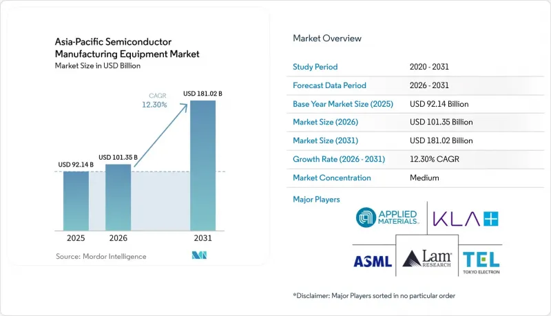
Mordor Intelligence에 의하면, 아시아태평양의 반도체 제조 장비 시장 규모는 2025년 921억 4,000만 달러로 평가되었습니다. 2026년에는 1,013억 5,000만 달러로 확대되어 2026년부터 2031년에 걸쳐 CAGR 12.30%로 성장을 지속하여, 2031년에는 1,810억 2,000만 달러에 이를 것으로 예측됩니다.
본 보고서는 장비 유형별(웨이퍼 팹 장비/프런트엔드 장비 등), 디바이스 유형별(로직 및 마이크로 컴포넌트, 메모리, 아날로그 등), 최종 사용자별(집적 디바이스 제조업체(IDM), 파운드리 등), 그리고 지역별(중국, 대만, 일본 등)로 분류되어 있습니다. 본 보고서에서는 상기 모든 부문에 대해 시장 규모 및 시장 가치(달러)에 대한 예측을 제시하고 있습니다.
아시아태평양의 반도체 제조 장비 시장 동향 및 인사이트
AI, HPC 및 HBM 생산 능력 확대
AI 및 고성능 컴퓨팅(HPC)으로 인해, 첨단 로직 및 HBM 생산 능력 확대 계획이 집중되어 있는 대만과 한국에서 장비 수요가 증가하고 있습니다. SEMI는 2026년부터 2028년까지 전 세계 300mm 팹 설비 투자액이 총 3,740억 달러에 달할 것으로 예측하고 있으며, 이는 AI 워크로드를 뒷받침하는 생산 능력에 대한 투자가 장기적으로 지속될 것임을 나타냅니다. 또한 SEMI는 같은 기간 DRAM 관련 설비 투자액이 790억 달러를 넘어설 것으로 예측하고 있으며, 이는 메모리 설비에 대한 수요가 AI 시스템에 대한 높아지는 요구 사항과 밀접하게 연관되어 있음을 보여줍니다. HBM 스택의 높이가 높아짐에 따라 성막, 에칭, TSV(실리콘 관통 비아), 본딩, 검사 및 테스트 공정이 추가됩니다. 이로 인해 메모리 생산량 단위당 장비 사용량이 증가하며, 공급업체는 계획된 생산 능력 확장에 대해 보다 명확한 전망을 얻을 수 있습니다. 아시아태평양의 반도체 제조 장비 시장은 이러한 프로그램을 뒷받침하는 해당 지역의 주요 로직 파운드리 및 메모리 제조업체들의 존재로 인해 혜택을 보고 있습니다.
GAA 및 2nm급 생산으로의 첨단 노드 전환
게이트 올 어라운드(GAA) 구조 및 2nm급 생산으로의 전환에 따라 리소그래피, 박막 형성, 에칭, 계측 및 검사 장비에 대한 수요가 증가하고 있습니다. TSMC는 2025년에 N2 기술의 양산을 시작했는데, 여기에는 기존 FinFET 설계보다 더 복잡한 공정 통합이 필요한 나노시트 트랜지스터가 채택되었습니다. 삼성은 로직 용도의 2nm GAA 제조를 위한 노력을 계속하고 있지만, 이를 위해서는 여전히 첨단 장비의 개발과 인증이 필요합니다. 첨단 노드 프로그램에서는 공정 윈도우의 엄격한 관리가 요구되며, 장비 성능, 공정 제어 및 현장 지원이 매우 중요합니다. 이러한 요구 사항으로 인해, 장기적인 인증 주기를 통해 팹과 협력할 수 있는 공급업체가 유리합니다. 대만, 한국, 일본이 첨단 노드 생산 및 관련 소재 공급에서 중심적인 역할을 수행하고 있어, 아시아태평양의 반도체 제조 장비 시장은 이러한 변화의 혜택을 누리고 있습니다.
수출 규제 및 기술 접근 제한
수출 규제로 인해 특정 최종 용도나 최종 사용자에 대한 특정 반도체 제조 장비, 부품, 소프트웨어 및 관련 기술에 대한 접근이 제한되고 있습니다. 미국 산업보안국(BIS)은 2024년에 반도체 제조 장비에 관한 규제를 발표하여 첨단 반도체 생산에 대한 제한을 확대했습니다. 이러한 제한은 공급업체의 판매 계획, 납기, 제품 구성, 고객 지원 및 규정 준수 절차에 영향을 미칠 수 있습니다. 또한, 이러한 규제는 기술 개발의 분화를 촉진하고 있어, 중국의 팹은 국산 장비에 대한 관심을 높이는 한편, 다른 지역의 팹은 확립된 국제적인 장비 플랫폼에 대한 접근을 유지하고 있습니다. 미국 의회조사국(CRS)은 동맹국 간의 협력이 반도체 관련 규제 적용 범위와 유효성에 영향을 미칩니다고 지적하고 있습니다. 아시아태평양의 반도체 제조 장비 시장은 첨단 장비에 대한 접근이 라이선싱 및 국경을 초월한 정책의 일관성에 의존하고 있기 때문에 고객 환경의 분절화가 진행되고 있습니다.
부문별 분석
2025년에는 프런트엔드 웨이퍼 제조 장비가 시장 점유율의 68.30%를 차지했습니다. 이는 로직 및 메모리 생산이 리소그래피, 증착, 에칭, 세정 및 공정 제어의 각 공정을 반복하는 데 의존하기 때문입니다. 첨단 노드의 공정 흐름에서는 이전 노드 세대에 비해 층에 대한 엄격한 제어와 더 빈번한 측정이 요구됩니다. 원자층 증착법 및 플라즈마 에칭은 나노시트 구조와 높은 종횡비(aspect ratio)를 가진 미세 구조에 중요합니다. 또한 공급업체들은 수율 향상을 위한 계측 및 검사 시스템도 제공합니다. 이러한 요구 사항으로 인해 프런트엔드 장비 조달은 장기적인 제조 관련 의사 결정이 됩니다.
칩 설계자들이 로직, 메모리, 상호 연결을 복잡한 패키지로 통합함에 따라, 조립 및 패키징 장비는 2031년까지 연평균 성장률(CAGR)이 14.50%에 달하며 가장 빠르게 성장하는 부문이 될 것으로 예측됩니다. 아시아태평양의 반도체 제조 장비 업계는 하이브리드 본딩, 웨이퍼 범프 형성, 성형, 검사, 다이싱 및 최종 테스트용 장비를 제공함으로써 이러한 수요에 대응하고 있습니다. 이종 통합에는 여러 다이 및 기판에 걸친 정확한 정렬과 결함 관리가 필요합니다. 또한, HBM 스택이나 AI 디바이스는 출하 전에 더욱 복잡한 검증이 필요하기 때문에 테스트 장비도 중요합니다. 팹 자동화, 화학약품 공급, 클린룸 시스템은 대량 생산을 수행하는 팹이 오염 및 자재 이동을 관리할 수 있도록 지원함으로써 이러한 설비 투자를 뒷받침하고 있습니다.
기타 혜택 :
- 엑셀 형식 시장 예측(ME) 시트
- 3개월간의 애널리스트 지원
자주 묻는 질문
목차
제1장 서론
제2장 조사 방법
제3장 개요
제4장 시장 구도
제5장 시장 규모 및 성장 예측
제6장 경쟁 구도
제7장 시장 기회 및 향후 전망
KTH 26.09.02According to Mordor Intelligence, the Asia-Pacific semiconductor manufacturing equipment market size is expected to grow from USD 92.14 billion in 2025 to USD 101.35 billion in 2026 and is forecast to reach USD 181.02 billion by 2031 at 12.30% CAGR over 2026-2031.
This report is Segmented by Equipment Type (Wafer Fab Equipment / Front-End Equipment, and More), by Device Type (Logic and Micro-Components, Memory, Analog, and More), by End-User (Integrated Device Manufacturers (IDMs), Foundries, and More), and by Geography (China, Taiwan, Japan, and More). The Report Offers Market Size and Value (USD) Forecasts for all the Above Segments.
Asia-Pacific Semiconductor Manufacturing Equipment Market Trends and Insights
AI, HPC, and HBM Capacity Expansion
AI and high-performance computing are raising equipment demand across Taiwan and South Korea, where advanced logic and HBM capacity programs are concentrated. SEMI expects global 300 mm fab equipment spending to total USD 374 billion from 2026 to 2028, signaling a sustained period of investment in capacity that supports AI workloads.SEMI also expects DRAM-related equipment investment to exceed USD 79 billion over the same period, linking demand for memory equipment to growing requirements for AI systems. Taller HBM stacks require additional deposition, etch, through-silicon-via, bonding, inspection, and test steps. This raises equipment content per unit of memory output and provides suppliers with greater visibility into planned capacity additions. The Asia-Pacific semiconductor manufacturing equipment market benefits from the region's key logic foundries and memory producers that serve these programs.
Advanced-Node Migration to GAA and 2 nm-Class Production
The move to gate-all-around structures and 2 nm-class production is increasing demand for lithography, deposition, etch, metrology, and inspection equipment. TSMC began volume production of its N2 technology in 2025, using nanosheet transistors that require more complex process integration than earlier FinFET designs. Samsung is continuing work on 2 nm GAA manufacturing for logic applications, which still requires the development and qualification of advanced equipment. Advanced-node programs need tightly controlled process windows, making tool performance, process control, and field support critical. These requirements favor suppliers that can work with fabs through long qualification cycles. The Asia-Pacific semiconductor manufacturing equipment market gains from this shift because Taiwan, South Korea, and Japan are central to advanced-node production and to the supply of supporting materials.
Export Controls and Technology-Access Restrictions
Export controls limit access to certain semiconductor manufacturing equipment, components, software, and related technology for specified end uses and end users. The United States Bureau of Industry and Security issued controls on semiconductor manufacturing equipment in 2024, expanding restrictions on advanced semiconductor production. These restrictions can alter supplier sales plans, delivery schedules, product configurations, customer support, and compliance processes. They also encourage separate technology paths, with Chinese fabs giving greater attention to domestic equipment while other regional fabs retain access to established international tool platforms. The Congressional Research Service notes that allied coordination affects the reach and effectiveness of semiconductor-related controls. The Asia-Pacific semiconductor manufacturing equipment market faces a more fragmented customer environment, as access to advanced tools depends on licensing and cross-border policy alignment.
Other drivers and restraints analyzed in the detailed report include:
- Government-Led Semiconductor Localization and Fab Incentives
- Advanced Packaging and Heterogeneous Integration
- Extreme Capital Intensity and Long Tool Payback Periods
For complete list of drivers and restraints, kindly check the Table Of Contents.
Segment Analysis
Front-end wafer fabrication equipment accounted for 68.30% of the market share in 2025 because logic and memory production depend on repeated lithography, deposition, etching, cleaning, and process-control steps. Advanced-node flows require tightly controlled layers and more frequent measurement than earlier node generations. Atomic layer deposition and plasma etch are important for nanosheet structures and high-aspect-ratio features. Suppliers also provide metrology and inspection systems to support yield learning. These requirements make front-end equipment procurement a long-term manufacturing decision.
Assembly and Packaging equipment is projected to be the fastest-growing segment, with a 14.50% CAGR through 2031 as chip designers integrate logic, memory, and interconnects into complex packages. The Asia-Pacific semiconductor manufacturing equipment industry is responding by providing tools for hybrid bonding, wafer bumping, molding, inspection, dicing, and final testing. Heterogeneous integration requires accurate alignment and defect control across multiple dies and substrates. Test equipment is also important because HBM stacks and AI devices need more complex validation before shipment. Fab automation, chemical delivery, and cleanroom systems support these purchases by helping high-volume fabs control contamination and material movement.
Complete Report Scope:
- By Equipment Type
- Wafer Fab Equipment / Front-End Equipment (lithography, deposition, etching, cleaning, CMP, thermal processing, front-end metrology & inspection equipment, etc.)
- Assembly and Packaging Equipment (die attach, wire bonding, flip-chip bonding, wafer bumping, thinning, dicing, molding, etc.)
- Semiconductor Test Equipment (automated test equipment, wafer probers, test handlers, burn-in equipment, and final test equipment)
- Fab Facility, Automation and Support Equipment (automation systems, wafer handling systems, AMHS, chemical & gas delivery systems, chillers, cleanroom support equipment, etc.)
- By Device Type
- Logic and Microcomponents (logic ICs, microprocessors, etc.)
- Memory (DRAM, NAND, HBM, NOR, etc.)
- Microprocessors (MPUs)
- Analog (Power management ICs, signal chain, interface Ics, etc.)
- Discrete and Power Devices (Diodes, transistors, MOSFETs, etc.)
- Sensors, MEMS and Optoelectronic Devices (Image sensors, MEMS sensors, etc.)
- By End User
- Integrated Device Manufacturers (IDMs)
- Foundries
- Outsourced Semiconductor Assembly and Test (OSAT) Companies
- Others (Research & Development (R&D) and Pilot Lines)
- By Geography
- China
- Taiwan
- South Korea
- Japan
- Singapore
- India
- Rest of Asia-Pacific
List of Companies Covered in this Report:
- Applied Materials, Inc.
- ASML Holding N.V.
- LAM RESEARCH CORPORATION
- Tokyo Electron Limited
- KLA Corporation
- SCREEN Holdings Co., Ltd.
- ADVANTEST CORPORATION
- Teradyne, Inc.
- Hitachi High-Tech Corporation
- ASM International N.V.
- Canon Inc.
- Nikon Corporation
- Onto Innovation Inc.
- Nova Ltd.
- DISCO Corporation
- BE Semiconductor Industries N.V.
- Kulicke & Soffa Industries, Inc.
- FormFactor, Inc.
- Veeco Instruments Inc.
- ASMPT Limited
- Kokusai Electric Corporation
- Advanced Micro-Fabrication Equipment Inc.
- Naura Technology Group Co., Ltd.
- Hanmi Semiconductor Co., Ltd.
- SuSS MicroTec SE
- EV Group
Additional Benefits:
- The market estimate (ME) sheet in Excel format
- 3 months of analyst support
TABLE OF CONTENTS
1 INTRODUCTION
- 1.1 Study Assumptions and Market Definition
- 1.2 Scope of the Study
2 RESEARCH METHODOLOGY
3 EXECUTIVE SUMMARY
4 MARKET LANDSCAPE
- 4.1 Market Overview
- 4.2 Market Drivers
- 4.2.1 AI, HPC and HBM Capacity Expansion
- 4.2.2 Advanced-Node Migration to GAA and 2 nm-Class Production
- 4.2.3 Government-Led Semiconductor Localization and Fab Incentives
- 4.2.4 Advanced Packaging and Heterogeneous Integration
- 4.2.5 China Equipment Localization and Mature-Node Capacity Build-Out
- 4.2.6 Equipment Demand from Power, Automotive and Compound Semiconductors
- 4.3 Market Restraints
- 4.3.1 Export Controls and Technology-Access Restrictions
- 4.3.2 Extreme Capital Intensity and Long Tool Payback Periods
- 4.3.3 Field-Service Talent and Applications-Engineering Bottlenecks
- 4.3.4 Qualification Delays for Domestic and Second-Source Tools
- 4.4 Value and Supply-Chain Analysis
- 4.5 Regulatory and Policy Landscape
- 4.6 Technology and Innovation Trends
- 4.7 Insights on Asia-Pacific Semiconductor Fab Expansion and Capacity Additions
- 4.8 Insights on AI and Automation in Semiconductor Manufacturing
- 4.9 Equipment Demand Outlook by Manufacturing Stage (Wafer fabrication, Assembly and packaging, Testing, Fab facility and automation)
- 4.10 Impact Assessment of Geopolitical Events on the Market
5 MARKET SIZE AND GROWTH FORECASTS
- 5.1 By Equipment Type
- 5.1.1 Wafer Fab Equipment / Front-End Equipment (lithography, deposition, etching, cleaning, CMP, thermal processing, front-end metrology & inspection equipment, etc.)
- 5.1.2 Assembly and Packaging Equipment (die attach, wire bonding, flip-chip bonding, wafer bumping, thinning, dicing, molding, etc.)
- 5.1.3 Semiconductor Test Equipment (automated test equipment, wafer probers, test handlers, burn-in equipment, and final test equipment)
- 5.1.4 Fab Facility, Automation and Support Equipment (automation systems, wafer handling systems, AMHS, chemical & gas delivery systems, chillers, cleanroom support equipment, etc.)
- 5.2 By Device Type
- 5.2.1 Logic and Microcomponents (logic ICs, microprocessors, etc.)
- 5.2.2 Memory (DRAM, NAND, HBM, NOR, etc.)
- 5.2.3 Microprocessors (MPUs)
- 5.2.4 Analog (Power management ICs, signal chain, interface Ics, etc.)
- 5.2.5 Discrete and Power Devices (Diodes, transistors, MOSFETs, etc.)
- 5.2.6 Sensors, MEMS and Optoelectronic Devices (Image sensors, MEMS sensors, etc.)
- 5.3 By End User
- 5.3.1 Integrated Device Manufacturers (IDMs)
- 5.3.2 Foundries
- 5.3.3 Outsourced Semiconductor Assembly and Test (OSAT) Companies
- 5.3.4 Others (Research & Development (R&D) and Pilot Lines)
- 5.4 By Geography
- 5.4.1 China
- 5.4.2 Taiwan
- 5.4.3 South Korea
- 5.4.4 Japan
- 5.4.5 Singapore
- 5.4.6 India
- 5.4.7 Rest of Asia-Pacific
6 COMPETITIVE LANDSCAPE
- 6.1 Market Concentration
- 6.2 Strategic Moves
- 6.2.1 Capacity Expansion and Localization Partnerships
- 6.2.2 Advanced-Node and Advanced-Packaging Collaborations
- 6.2.3 Product Launches and Platform Extensions
- 6.2.4 Mergers, Acquisitions and Minority Investments
- 6.3 Market Share Analysis
- 6.4 Company Profiles (Includes Global Level Overview, Market Level Overview, Core Segments, Financials as available, Strategic Information, Products and Services, Recent Developments)
- 6.4.1 Applied Materials, Inc.
- 6.4.2 ASML Holding N.V.
- 6.4.3 LAM RESEARCH CORPORATION
- 6.4.4 Tokyo Electron Limited
- 6.4.5 KLA Corporation
- 6.4.6 SCREEN Holdings Co., Ltd.
- 6.4.7 ADVANTEST CORPORATION
- 6.4.8 Teradyne, Inc.
- 6.4.9 Hitachi High-Tech Corporation
- 6.4.10 ASM International N.V.
- 6.4.11 Canon Inc.
- 6.4.12 Nikon Corporation
- 6.4.13 Onto Innovation Inc.
- 6.4.14 Nova Ltd.
- 6.4.15 DISCO Corporation
- 6.4.16 BE Semiconductor Industries N.V.
- 6.4.17 Kulicke & Soffa Industries, Inc.
- 6.4.18 FormFactor, Inc.
- 6.4.19 Veeco Instruments Inc.
- 6.4.20 ASMPT Limited
- 6.4.21 Kokusai Electric Corporation
- 6.4.22 Advanced Micro-Fabrication Equipment Inc.
- 6.4.23 Naura Technology Group Co., Ltd.
- 6.4.24 Hanmi Semiconductor Co., Ltd.
- 6.4.25 SuSS MicroTec SE
- 6.4.26 EV Group
7 MARKET OPPORTUNITIES AND FUTURE OUTLOOK
- 7.1 White-Space and Unmet-Need Assessment