
|
시장보고서
상품코드
2044001
실리콘 웨이퍼상 질화갈륨 : 시장 점유율 분석, 산업 동향 및 통계 데이터, 성장 예측(2026-2031년)Gallium Nitride (GaN) On Silicon Wafer - Market Share Analysis, Industry Trends & Statistics, Growth Forecasts (2026 - 2031) |
||||||
 Mordor Intelligence
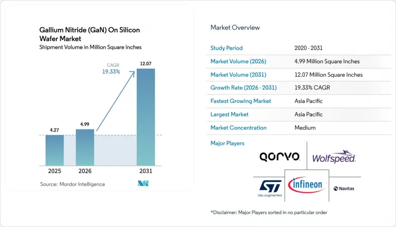
실리콘 웨이퍼상 질화갈륨 시장 규모는 2025년 427만 평방인치로 평가되었습니다. 2026년에는 499만 평방인치로 확대되어 2031년까지 1,207만 평방인치에 이를 것으로 예상되며 2026년부터 2031년에 걸쳐 CAGR 19.33%를 나타낼 전망입니다.
기존 실리콘에서 광대역 갭 설계로의 꾸준한 전환으로 더 높은 스위칭 주파수, 향상된 열전도율, 입방인치당 3kW 이상의 전력 밀도를 달성할 수 있게 되었습니다. OEM 업체들은 800V 전기차용 트랙션 인버터, 의무화된 USB-C Power Delivery 3.1 고속 충전 표준 및 위성 기반 5G 비지상 네트워크 구축에 대응하기 위해 200mm GaN-on-Si의 인증을 서두르고 있습니다. 집적 장치 제조업체, 파운드리 및 팹리스 스타트업들이 고속 충전 어댑터, 데이터센터용 전원 공급 장치, LiDAR 드라이버 설계 주문을 받으면서 경쟁 압력이 증가하고 있습니다. 한편, 북미와 유럽의 정부 보조금으로 인해 300mm 파일럿 라인 구축이 가속화되어 상용화 일정이 단축되고 있습니다.
세계의 실리콘 웨이퍼상 질화갈륨 시장 동향과 인사이트
성숙해가는 200mm GaN-on-Si 생산 라인
2025년, 여러 디바이스 제조업체들이 200mm GaN-on-Si 웨이퍼의 인증을 획득하여 다이 비용을 절감하고 생산량을 확대할 수 있게 되었습니다. 인피니언은 2025년 하반기부터 300mm GaN 파워 디바이스의 고객용 샘플 공급을 시작했으며, 2026년 말까지 양산을 목표로 하고 있습니다. 이노사이언스는 2025년까지 8인치 라인의월생산량을 2만장까지 확대할 계획이며, 2030년까지 7만장까지 생산량을 늘릴 예정입니다. Navitas와 PSMC는 2025년 4분기에 200mm 웨이퍼 인증을 완료했고, 2026년 상반기에 생산을 본격화할 예정입니다. 이러한 움직임은 리드 타임을 단축하고, 듀얼 소싱을 지원하며, 자동차, 산업 및 소비자 부문에서의 채택을 촉진할 것입니다. 실리콘 웨이퍼상 질화갈륨 시장은 규모의 경제가 향상됨에 따라 슈퍼정션 실리콘과의 비용 패리티의 혜택을 누리고 있습니다.
MOCVD 처리량 증가로 인한 에피택셜 웨이퍼 비용 감소
각 장비 업체들은 처리량을 최대 60%까지 향상시킬 수 있는 멀티 웨이퍼 플래니터리 리액터를 출시하고 있으며, 이를 통해 2년 이내에 에피택셜 비용을 약 1/3로 줄일 수 있습니다. Veeco의 Propel 플랫폼은 한 번에 8장의 200mm 웨이퍼를 처리할 수 있으며, 인사이치 측정 기능을 통해 공정 제어를 엄격하게 제어할 수 있습니다. AIXTRON의 G5+C는 사이클당 19장의 웨이퍼를 처리하여 사이클 시간을 단축하고 수율을 향상시킵니다. 비용 절감으로 그동안 부품 원가에 민감했던 USB-C 어댑터, 무선 충전기 등 민수용으로의 전개가 가능해졌습니다. 팹리스 업체들은 이제 대량 생산 설계에 진입할 수 있게 되어 실리콘 웨이퍼상 질화갈륨 시장 점유율을 엔트리 레벨 가격대까지 확대되고 있습니다.
8인치 이상의 크기에서 수율에 영향을 미치는 스레딩 변위
실리콘의 이종 에피택셜 성장에서는 스레딩 전위가 발생하여 내압을 감소시키고 누설 전류를 증가시킵니다. 200mm 웨이퍼에서 1×108cm-2에서 5×108cm-2의 변위 밀도가 지속되며, 초기 로트에서 수율을 최대 20%까지 감소시킵니다. 300mm 웨이퍼에서는 열 구배가 길어지기 때문에 에지 응력 및 휨이 악화되어 인증 시험 및 설비 투자 기간이 길어집니다. 디바이스 제조업체들은 그라데이션 AlGaN 버퍼와 인시츄 질화물 중간층을 도입하고 있지만, 학습 곡선으로 인해 실리콘 웨이퍼상 질화갈륨 시장의 성장 속도는 둔화되고 있습니다.
부문 분석
2025년 출하량 중 150mm 포맷이 53.92%를 차지했습니다. 이는 성숙한 에피택셜 공정과 감가상각이 완료된 장비 기반이 매력적인 경제성을 뒷받침했기 때문입니다. 그러나 200mm 포맷은 2031년까지 연평균 복합 성장률(CAGR) 20.37%를 나타낼 것으로 예측되며, 수율 곡선이 성숙해지면 다이 비용을 35-45% 절감할 수 있을 것으로 예측됩니다. 온세미는 Innoscience 및 GlobalFoundries와의 제휴를 통해 200mm 듀얼 소스 생산 능력을 확보하고 있으며, 2026년 상반기에 샘플 제공이 예정되어 있습니다. 따라서 실리콘 웨이퍼상 질화갈륨 시장은 200mm가 주류로 전환되고 있으며, 100mm는 조사 및 소량의 국방 수요에 국한될 것으로 보입니다.
인피니언이 2025년 10월부터 300mm GaN 고객용 샘플을 제공하기 시작한 것은 자동차 및 산업용 양산을 염두에 둔 적극적인 스케일업 로드맵을 뒷받침하는 것입니다. imec의 300mm 파일럿 라인은 GaN과 첨단 CMOS를 통합하여 단일 칩 전력 관리 IC를 목표로 하고 있습니다. 초기 성공 여부는 웨이퍼의 휨과 스레딩 변위를 줄일 수 있는지에 달려 있습니다. 공정 제어에 성공하면, 300mm 실리콘 기판 위 GaN(질화갈륨) 웨이퍼 시장 규모 우위는 과거 실리콘의 비용 곡선을 재현하고, 상품화를 가속화할 수 있습니다.
실리콘 기판상의 GaN 웨이퍼상의 GaN은 2025년 생산량의 57.49%를 차지했으며, 200mm 및 300mm 실리콘 팹과의 호환성 및 공통 전구체 공급망에 힘입어 2031년까지 연평균 19.78%의 성장률을 나타낼 것으로 전망됩니다. 이러한 원가 우위는 대량 생산되는 소비자 및 자동차용 용도를 지원하며 실리콘 웨이퍼상 질화갈륨 시장에서 지배적인 위치를 확고히 하고 있습니다. 반면, 실리콘 카바이드(SiC) 기판상의 GaN은 열전도율이 우수하고 성능이 4배의 가격 프리미엄을 상회하는 군용 레이더나 위성 트랜스폰더와 같은 틈새 용도에 국한되어 있습니다.
사파이어 기판상의 GaN은 광전자 산업, 특히 마이크로 LED 및 자외선 발광 소자에 계속 활용되고 있습니다. 순수 GaN 기판은 가장 낮은 전위밀도를 실현하지만, 소규모 연구용 로트 이상의 규모에서는 비용이 너무 높아 실용화가 어렵습니다. 그 결과, 시장 진출기업들은 GaN-on-silicon의 신뢰성을 높이고 지원 전압을 최대 1,200V까지 확장하는 초격자 버퍼 기술 혁신에 연구개발(R&D)을 집중하고 있으며, 이에 따라 실리콘 웨이퍼상 질화갈륨 시장 점유율은 여전히 실리콘이 확고한 지위를 유지하고 있습니다.
"실리콘 웨이퍼상 질화갈륨 시장 보고서는 웨이퍼 직경(100mm, 150mm, 200mm), 기판 유형(실리콘 기판 상 GaN, 실리콘 카바이드 기판 상 GaN 등), 디바이스 용도(파워 일렉트로닉스, 무선 주파수 디바이스 등), 최종 용도(자동차, EV, 항공우주, 방위산업, 기타), 지역별로 구분하여 조사하였습니다. 산업(자동차/EV, 항공우주/국방, 기타) 및 지역별로 분류되어 있습니다. 시장 예측은 수량(평방인치) 기준으로 제공됩니다.
지역별 분석
아시아태평양은 2025년 출하량의 62.53%를 차지하며 2031년까지 연평균 20.27% 성장할 것으로 예측됩니다. 중국은 5년 내월7만 장의 웨이퍼 생산을 목표로 하는 Innoscience의 계획을 지원하고 있으며, 대만은 모바일 및 자동차용 제품에 GaN-CMOS 통합을 모색하고 있습니다. 일본은 ROHM, 도시바, 미쓰비시전기의 수십 년간의 화합물 반도체 전문성을 활용하고 있으며, 한국은 데이터센터와 5G 전력 모듈을 타겟으로 하고 있습니다. 인도는 파일럿 라인에 대한 특혜를 제공하고 있지만, 상업 생산은 아직 초기 단계에 있기 때문에 실리콘 기판상의 GaN(질화갈륨) 웨이퍼 시장은 여전히 동아시아 생태계를 중심으로 발전하고 있습니다.
북미는 'CHIPS and Science Act'에 의한 520억 달러의 자금 지원의 혜택을 받고 있습니다. MACOM은 GaN-on-SiC RF 라인에 대한 예비 지원을 확보했으며, 이는 광대역 갭 반도체 공급 확보에 대한 연방 정부의 이니셔티브을 강조하고 있습니다. 미국의 파운드리 업체는 팹리스 스타트업과 협력하여 자동차 등급 GaN 장치를 개발하고 있으며, 캐나다는 북극권 감시 레이더 프로그램을 추진하고 있습니다. 멕시코 조립공장은 전기자동차 공장과 같은 부지에 설치되어 실리콘 기판 상 질화갈륨(GaN) 웨이퍼 시장에서의 지역화 이점을 확대되고 있습니다.
유럽에서는 EU CHIPS 법에 따른 430억 유로의 자금과 IPCEI 마이크로일렉트로닉스 보조금 81억 유로를 활용하여 인피니언의 300mm 파일럿 라인과 프라운호퍼의 광대역 갭 프로젝트에 자본을 투입하는 등 진전을 이루고 있습니다. 프랑스는 초광대역갭 재료 관련 IPCEI 클러스터를 주도하고 있으며, 영국은 위성통신용 RF 디바이스에 집중하고 있습니다. 네덜란드의 ASML은 GaN 패터닝을 위한 리소그래피 장비를 개발하고 있으며, 이탈리아는 ST마이크로일렉트로닉스의 MasterGaN 플랫폼을 추진하고 있습니다. 주요 3개국을 제외한 남미, 중동 및 아프리카는 아직 개발 단계에 머물러 있으며, 브라질과 아랍에미레이트에서는 GaN을 이용한 재생에너지 관련 시범 프로젝트가 산발적으로 진행되고 있는 정도입니다.
기타 혜택 :
- 엑셀 형식 시장 예측(ME) 시트
- 3개월간 애널리스트 지원
자주 묻는 질문
목차
제1장 서론
제2장 분석 방법
제3장 주요 요약
제4장 시장 구도
제5장 시장 규모 및 성장률 예측
제6장 경쟁 구도
제7장 시장 기회와 향후 전망
KTH 26.05.29The Gallium Nitride (GaN) on Silicon Wafer market size is expected to increase from 4.27 million square inches in 2025 to 4.99 million square inches in 2026 and reach 12.07 million square inches by 2031, growing at a CAGR of 19.33% over 2026-2031.
Robust migration from legacy silicon toward wide-bandgap designs is enabling higher switching frequencies, elevated thermal conductivity, and power densities above 3 kW per cubic inch. Original equipment manufacturers are fast-tracking 200 mm GaN-on-Si qualification in response to 800-volt electric-vehicle traction inverters, mandated USB-C Power Delivery 3.1 fast-charging rules, and satellite-based 5G non-terrestrial network rollouts. Competitive pressure is intensifying as integrated device manufacturers, foundries, and fabless start-ups secure design wins in fast-charging adapters, data-center power supplies, and lidar drivers, while government subsidies in North America and Europe accelerate 300 mm pilot lines and compress commercialization timelines.
Global Gallium Nitride (GaN) On Silicon Wafer Market Trends and Insights
Maturing 200 mm GaN-on-Si Fabrication Lines
Multiple device makers qualified 200 mm GaN-on-Si wafers during 2025, cutting die costs and enabling higher unit volumes. Infineon began customer sampling of 300 mm GaN power devices in late 2025 and targets production by end-2026. Innoscience plans to scale to 20,000 wafers per month on 8-inch lines by 2025 and reach 70,000 by 2030. Navitas and PSMC completed 200 mm qualification in fourth-quarter 2025 and will ramp production in first-half 2026. These moves shorten lead times, support dual-sourcing, and spur adoption in automotive, industrial, and consumer segments. The Gallium Nitride (GaN) on Silicon Wafer market benefits from cost parity with super-junction silicon as scale economies improve.
Falling Epi-Wafer Costs Due to Higher MOCVD Throughput
Tool vendors have released multi-wafer planetary reactors that raise throughput by up to 60%, lowering epitaxial costs by roughly one-third within two years. Veeco's Propel platform processes eight 200 mm wafers per run with in-situ metrology for tighter process control. AIXTRON's G5+C handles 19 wafers per cycle, reducing cycle time and boosting yield. Lower costs open consumer applications such as USB-C adapters and wireless chargers that were previously bill-of-materials sensitive. Fabless firms can now bid for high-volume designs, expanding the Gallium Nitride (GaN) on Silicon Wafer market footprint across entry-level price points.
Threading Dislocations Impacting Yield Beyond 8 inch
Heteroepitaxial growth on silicon introduces threading dislocations, which degrade the breakdown voltage and increase leakage. Dislocation densities of 1X108 cm-2 to 5X108 cm-2 persist at 200 mm, trimming yields by up to 20% in early lots. Longer thermal gradients at 300 mm worsen edge stress and bow, extending qualification and capex. Device makers are adding graded AlGaN buffers and in-situ nitride interlayers, yet the learning curve slows the Gallium Nitride (GaN) on Silicon Wafer market ramp.
Other drivers and restraints analyzed in the detailed report include:
- Surge in 800 V Electric-Vehicle Powertrain Architectures
- Mandatory USB-C PD 3.1 240 W Fast-Charging Adoption
- Limited Availability of 8 inch GaN Growth Tools
For complete list of drivers and restraints, kindly check the Table Of Contents.
Segment Analysis
The 150 mm format accounted for 53.92% of shipments in 2025 as mature epitaxial recipes and depreciated tool bases supported attractive economics. However, the 200 mm tier is projected to register a 20.37% CAGR through 2031, providing 35-45% die cost savings once yield curves mature. onsemi secured dual-source 200 mm capacity through partnerships with Innoscience and GlobalFoundries, with samples due in first-half of 2026. The Gallium Nitride (GaN) on Silicon Wafer market therefore pivots toward 200 mm as mainstream, while 100 mm remains limited to research and low-volume defense needs.
Infineon's customer sampling of 300 mm GaN in October 2025 underscores an aggressive scaling roadmap aimed at automotive and industrial volumes. imec's 300 mm pilot line integrates GaN with advanced CMOS to target single-chip power-management ICs. Early success will depend on mitigating wafer bow and threading dislocations. If process control succeeds, Gallium Nitride (GaN) on Silicon Wafer market size advantages at 300 mm could replicate historical silicon cost curves and accelerate commoditization.
GaN-on-silicon held 57.49% of 2025 volume and is forecast to grow at 19.78% through 2031, anchored by compatibility with 200 mm and 300 mm silicon fabs and shared precursor supply chains. This cost leadership underpins high-volume consumer and automotive applications, reinforcing dominance within the Gallium Nitride (GaN) on Silicon Wafer market. GaN-on-silicon carbide, despite superior thermal conductivity, remains niche for military radar and satellite transponders where performance trumps a four-fold price premium.
GaN-on-sapphire continues to serve the optoelectronics industry, especially micro-LEDs and ultraviolet emitters. Native GaN substrates deliver the lowest dislocation densities but are cost-prohibitive beyond small research lots. Consequently, market participants allocate R&D to superlattice buffer innovations that raise GaN-on-silicon reliability and extend its addressable voltage up to 1,200 V, keeping the Gallium Nitride (GaN) on Silicon Wafer market share firmly in silicon's corner.
The Gallium Nitride (GaN) On Silicon Wafer Market Report is Segmented by Wafer Diameter (100 Mm, 150 Mm, and 200 Mm), Substrate Type (GaN-On-Silicon, GaN-On-Silicon Carbide, and More), Device Application (Power Electronics, Radio-Frequency Devices, and More), End-Use Industry (Automotive and EV, Aerospace and Defense, and More), and Geography. The Market Forecasts are Provided in Terms of Volume (Square Inches).
Geography Analysis
Asia-Pacific accounted for 62.53% of 2025 volume and is slated to grow at a 20.27% CAGR through 2031. China backs Innoscience's plan to reach 70,000 wafers per month over five years, while Taiwan explores GaN-CMOS integration for mobile and automotive products. Japan leverages decades of compound semiconductor expertise at ROHM, Toshiba, and Mitsubishi Electric, whereas South Korea targets data center and 5G power modules. India offers incentives for pilot lines, but commercial output remains embryonic, so the Gallium Nitride (GaN) on Silicon Wafer market continues to center on East-Asian ecosystems.
North America benefits from USD 52 billion in CHIPS and Science Act funding. MACOM secured preliminary support for a GaN-on-SiC RF line, highlighting the federal commitment to the security of wide-bandgap supply. U.S. foundries collaborate with fabless start-ups to build automotive-grade GaN devices, while Canada advances Arctic surveillance radar programs. Mexican assembly sites co-locate with electric-vehicle plants, extending regionalization advantages within the Gallium Nitride (GaN) on Silicon Wafer market.
Europe advances through EUR 43 billion in EU CHIPS Act resources and EUR 8.1 billion in IPCEI microelectronics grants, funneling capital to Infineon's 300 mm pilot line and Fraunhofer wide-bandgap projects. France heads an IPCEI cluster on ultra-wide-bandgap materials, and the United Kingdom focuses on RF devices for satellite links. ASML in the Netherlands explores lithography tooling for GaN patterning, while Italy promotes STMicroelectronics' MasterGaN platform. Outside the core triad, South America, the Middle East, and Africa remain nascent, with isolated renewable-energy pilots using GaN in Brazil and the United Arab Emirates.
- Wolfspeed Inc.
- Qorvo Inc.
- NXP Semiconductors N.V.
- Infineon Technologies AG
- STMicroelectronics N.V.
- Renesas Electronics Corporation
- Efficient Power Conversion (EPC) Corp.
- Transphorm Inc.
- Toshiba Electronic Devices and Storage Corp.
- ROHM Co., Ltd.
- Navitas Semiconductor Corp.
- Innoscience (Suzhou) Technology Co., Ltd.
- MACOM Technology Solutions Holdings Inc.
- ON Semiconductor Corp.
- GaN Systems Inc.
- Power Integrations Inc.
- Skyworks Solutions Inc.
- Mitsubishi Electric Corp.
- Sumitomo Electric Industries Ltd.
- Integra Technologies Inc.
Additional Benefits:
- The market estimate (ME) sheet in Excel format
- 3 months of analyst support
TABLE OF CONTENTS
1 INTRODUCTION
- 1.1 Study Assumptions and Market Definition
- 1.2 Scope of the Study
2 RESEARCH METHODOLOGY
3 EXECUTIVE SUMMARY
4 MARKET LANDSCAPE
- 4.1 Market Overview
- 4.2 Industry Value-Chain Analysis
- 4.3 Technological Outlook
- 4.4 Impact of Macroeconomic Factors on the Market
- 4.5 Market Drivers
- 4.5.1 Maturing 200 Mm GaN-on-Si Fabrication Lines
- 4.5.2 Falling Epi-Wafer Costs Due To Higher MOCVD Throughput
- 4.5.3 Surge In 800 V EV Powertrain Architectures
- 4.5.4 Mandatory USB-C PD3.1 240 W Fast-Charging Adoption
- 4.5.5 Rising Deployment Of Satellite-Based 5G NTN Backhaul
- 4.5.6 Government Incentives For Wide-Bandgap Fabs (CHIPS, EU IPCEI)
- 4.6 Market Restraints
- 4.6.1 Threading Dislocations Impacting Yield Beyond 8 Inch
- 4.6.2 Limited Availability Of 8 Inch GaN Growth Tools
- 4.6.3 IP Cross-Licensing Barriers Among IDMs and Foundries
- 4.6.4 Thermal Mismatch Induced Wafer Bow At ?200 mm
- 4.7 Porter's Five Forces Analysis
- 4.7.1 Threat of New Entrants
- 4.7.2 Bargaining Power of Suppliers
- 4.7.3 Bargaining Power of Buyers
- 4.7.4 Threat of Substitutes
- 4.7.5 Competitive Rivalry
5 MARKET SIZE AND GROWTH FORECASTS (VOLUME)
- 5.1 By Wafer Diameter
- 5.1.1 100 mm (4 inch)
- 5.1.2 150 mm (6 inch)
- 5.1.3 200 mm (8 inch)
- 5.2 By Substrate Type
- 5.2.1 GaN-on-Silicon
- 5.2.2 GaN-on-Silicon Carbide
- 5.2.3 GaN-on-Sapphire
- 5.2.4 Native GaN (Bulk)
- 5.3 By Device Application
- 5.3.1 Power Electronics
- 5.3.2 Radio-Frequency Devices
- 5.3.3 Optoelectronics (LED and Laser)
- 5.3.4 Other Applications
- 5.4 By End-Use Industry
- 5.4.1 Automotive and EV
- 5.4.2 Aerospace and Defense
- 5.4.3 Renewable Energy and Storage
- 5.4.4 Consumer Electronics
- 5.4.5 Telecommunications
- 5.4.6 Industrial Power Systems
- 5.5 By Geography
- 5.5.1 North America
- 5.5.1.1 United States
- 5.5.1.2 Canada
- 5.5.1.3 Mexico
- 5.5.2 Europe
- 5.5.2.1 Germany
- 5.5.2.2 United Kingdom
- 5.5.2.3 France
- 5.5.2.4 Rest of Europe
- 5.5.3 Asia-Pacific
- 5.5.3.1 China
- 5.5.3.2 Japan
- 5.5.3.3 India
- 5.5.3.4 South Korea
- 5.5.3.5 Taiwan
- 5.5.3.6 Rest of Asia-Pacific
- 5.5.4 South America
- 5.5.5 Middle East
- 5.5.6 Africa
- 5.5.1 North America
6 COMPETITIVE LANDSCAPE
- 6.1 Market Concentration
- 6.2 Strategic Moves
- 6.3 Market Share Analysis
- 6.4 Company Profiles (includes Global Level Overview, Market Level Overview, Core Segments, Financials as available, Strategic Information, Market Rank/Share, Products and Services, Recent Developments)
- 6.4.1 Wolfspeed Inc.
- 6.4.2 Qorvo Inc.
- 6.4.3 NXP Semiconductors N.V.
- 6.4.4 Infineon Technologies AG
- 6.4.5 STMicroelectronics N.V.
- 6.4.6 Renesas Electronics Corporation
- 6.4.7 Efficient Power Conversion (EPC) Corp.
- 6.4.8 Transphorm Inc.
- 6.4.9 Toshiba Electronic Devices and Storage Corp.
- 6.4.10 ROHM Co., Ltd.
- 6.4.11 Navitas Semiconductor Corp.
- 6.4.12 Innoscience (Suzhou) Technology Co., Ltd.
- 6.4.13 MACOM Technology Solutions Holdings Inc.
- 6.4.14 ON Semiconductor Corp.
- 6.4.15 GaN Systems Inc.
- 6.4.16 Power Integrations Inc.
- 6.4.17 Skyworks Solutions Inc.
- 6.4.18 Mitsubishi Electric Corp.
- 6.4.19 Sumitomo Electric Industries Ltd.
- 6.4.20 Integra Technologies Inc.
7 MARKET OPPORTUNITIES AND FUTURE OUTLOOK
- 7.1 White-Space and Unmet-Need Assessment