
|
시장보고서
상품코드
2044055
GaN 기반 LED 에피텍셜 웨이퍼 시장 : 점유율 분석, 산업 동향 및 통계, 성장 예측(2026-2031년)GaN-Based LED Epitaxial Wafers - Market Share Analysis, Industry Trends & Statistics, Growth Forecasts (2026 - 2031) |
||||||
GaN 기반 LED 에피텍셜 웨이퍼 시장 규모는 2026년 13억 5,000만 달러에서 2031년까지 21억 5,000만 달러로 확대되어 2026년부터 2031년까지 CAGR 9.75%를 나타낼 것으로 예측되고 있습니다.

금속유기화학기상증착(MOCVD) 플랫폼의 성숙, 미니 LED 및 마이크로 LED 디스플레이의 채택 가속화, 전기자동차 헤드램프의 채택 확대에 따라 수요가 증가하고 있습니다. 공급업체들은 범용 조명용 웨이퍼의 생산 능력을 보다 엄격한 파장 균일성 및 결함 기준이 요구되는 고부가가치 광전자, 센싱 및 자동차 기판용으로 전환하고 있습니다. 장비 제조업체들은 200mm 및 300mm 포맷에서 비용 우위를 점하고 있으며, 수직 통합형 아태지역 기업들은 업스트림 공정의 결정 성장 제어와 다운스트림 공정의 패키징을 활용하여 개발 주기를 단축하고 있습니다.
세계 GaN 기반 LED 에피택셜 웨이퍼 시장 동향 및 인사이트
미니 LED 및 마이크로 LED 디스플레이의 급속한 대중화
디스플레이 제조업체들은 OLED의 번트 현상을 극복하고 더 높은 피크 밝기를 구현하기 위해 Mini-LED 및 Micro-LED 개발 프로그램을 가속화하고 있으며, 이로 인해 직경 200mm 및 300mm 기판에서 파장 균일성이 5nm 미만인 웨이퍼에 대한 수요가 증가하고 있습니다. Ennostar는 ALLOS Semiconductors와 공동으로 2,000 PPI 이상의 웨어러블 디스플레이를 위한 200mm GaN-on-Si 프로젝트를 발표했습니다. 애플은 미래의 웨어러블 디스플레이를 위한 수직 통합형 에피택셜 공급을 확보하기 위해 신주쿠 과학단지에 AU Optronics와 Epistar에 3억 3,400만 달러를 투자했습니다. NIO ET9에 탑재된 ams OSRAM의 EVIYOS HD25 모듈에서 자동차 분야와의 상호 교류가 두드러지게 나타납니다. 이 모듈은 25,600개의 마이크로 LED 픽셀을 내장하고 있으며, 500m의 투사 거리를 구현하기 위해 디스플레이급 에피택시 기술을 필요로 합니다.
전기차 전조등 생산 확대
전기자동차 제조업체들은 1만 픽셀 이상의 어댑티브 헤드램프 사양을 요구하고 있으며, 엄격한 AEC-Q 사이클을 견딜 수 있는 결함이 적고 고휘도 웨이퍼를 요구하고 있습니다. EVIYOS HD25는 투사 거리를 400m에서 500m로 연장하고, 중속 주행 시 로우빔 밝기를 50% 향상시켜 이에 필요한 웨이퍼의 성능 도약을 여실히 보여주고 있습니다. 현재 프리미엄 EV에는 100개 이상의 LED 패키지가 탑재되어 있으며, 각 패키지에는 광범위한 온도 변화에도 색 안정성을 유지해야 하는 에피택셜 소재가 사용됩니다.
자본 집약적인 MOCVD 장비 업그레이드
최첨단 300mm GaN 원자로는 대당 500만 달러 이상이며, 본격적인 생산 클러스터에는 8-10개의 장비와 함께 인사이트 측정 장치 및 로봇 시스템이 필요합니다. Veeco는 2026년 Propel300의 매출이 8,000만 달러에 달할 것으로 예상하고 있으며, 이는 현재 극소수의 팹만이 이러한 자본을 흡수할 수 있음을 시사합니다. 중소형 에피택셜 웨이퍼 공급업체는 전략적 딜레마에 직면해 있습니다. 기존 150mm 및 200mm MOCVD 장비는 감가상각이 완료되어 경쟁력 있는 현금 비용으로 웨이퍼를 생산할 수 있지만, 이러한 플랫폼은 300mm 포맷의 "웨이퍼 당 다이 수"의 경제성에 미치지 못하며, 대형 파운드리 업체들이 규모를 확대함에 따라 이에 따라 수익률 압박 리스크가 발생하게 됩니다.
부문 분석
150mm 이하 웨이퍼는 2025년 매출의 68.71%를 차지해, 이는 일반 조명 붐기에 구축된 기존 MOCVD 장비군을 반영합니다. 파운드리 업체들이 다이 수 경제성과 실리콘 CMOS 라인과의 호환성을 추구하면서 300mm 기판용 GaN 기반 LED 에피택셜 웨이퍼 시장 규모는 CAGR 10.89%로 확대될 것으로 예측됩니다. 300mm 생태계가 성숙할 때까지 중간 크기의 200mm 포맷이 현재 디스플레이용 백라이트 수요를 채우고 있으며, 마이크로 LED 웨어러블 기기를 위한 Ennostar-ALLOS 프로젝트가 그 좋은 예입니다. 300mm로의 전환은 전력 및 RF 분야에서 가장 두드러지며, GaN과 CMOS 드라이버를 하나의 웨이퍼에 공동 집적함으로써 모듈의 실적와 비용을 절감할 수 있습니다. 그러나 직경이 커질수록 열의 불균일성이 악화되어 고도의 셉타 설계와 실시간 온도 측정이 요구됩니다.
비용의 변동은 업스트림로 파급되고 있습니다. 현재 기판 벤더는 보다 엄격한 평탄도 및 표면 거칠기 사양을 충족하는 300mm 사파이어 및 실리콘 웨이퍼를 공급해야 합니다. ROHM 반도체와 TSMC가 2026년 2월 체결한 제휴는 기존 300mm 클린룸 시설을 활용하여 GaN 파워 디바이스를 공동 개발하는 것으로, 인프라 공유가 가져다주는 이점을 강조하고 있습니다. 그러나 많은 설비 투자와 자동차 인증의 장기화로 인해 예측 기간 동안 300mm의 광범위한 채택은 충분한 자금력을 갖춘 팹에 국한될 것으로 예측됩니다.
2025년에는 미니 LED 백라이트와 일반 조명을 주축으로 한 광전자 분야가 매출의 44.28%를 차지해 선두를 유지했지만, 수직공진기면발광레이저(VCSEL)와 LiDAR 광원의 보급으로 센서 분야는 CAGR 10.97%를 나타낼 것으로 예측됩니다. 를 기록할 것으로 예측됩니다. 개별 전력 장치용 GaN 기반 LED 에피택셜 웨이퍼 시장 점유율은 결함 밀도보다 가격을 우선시하는 비용 중심의 충전기 용도에 의해 제한되어 보다 완만한 속도로 증가하고 있습니다.
센서 분야의 급속한 성장은 첨단 운전자 보조 시스템(ADAS)을 의무화하는 자동차 안전 규제와 스마트폰 및 웨어러블 기기의 얼굴인식 및 증강현실(AR) 기능에 대한 소비자 수요의 결합을 반영합니다. 마이크로 부문은 마이크로 전자기계 시스템(MEMS)과 마이크로 스케일 광소자를 포함하며, 향후 성장이 기대되는 분야로 부상하고 있습니다. 현재 생산량은 제한적이지만, GaN 기반 마이크로 공진기 및 광 집적 회로가 칩 스케일 광 검출 및 거리 측정(LiDAR)을 가능하게 하는 잠재력은 초저결함 에피택셜 웨이퍼에 대한 새로운 수요의 원천이 될 수 있습니다. 옵토일렉트로닉스가 계속 주류가 될 것으로 예상되지만, 센싱 수요가 가속화됨에 따라 그 우위는 줄어들고 있습니다.
지역별 분석
아시아태평양은 2025년 매출의 56.27%를 차지해, 대만의 수직 통합 클러스터와 중국의 보조금에 의한 생산 능력 확대에 힘입어 연평균 10.73%의 성장률을 보일 것으로 예측됩니다. 에피스타, 렉스타, 에노스타 등 대만 기업들은 패널 조립업체와 밀접하게 사업을 전개하고 있으며, 마이크로 LED 생산에 필수적인 피드백 루프를 가속화하고 있습니다. 중국의 유력 기업인 산안광전(Sanan Optoelectronics)은 국가 인센티브와 유럽과 미국 자동차 판로 개척을 위한 루미레드(Lumileds) 인수 계획에 힘입어 적극적으로 사업 규모를 확대되고 있습니다.
북미와 유럽은 수요에서 차지하는 비중은 작지만 전략적으로 중요한 역할을 하고 있습니다. 미국 에너지부(DOE)의 자금 지원은 새로운 에피택셜 제조 공정의 초기 단계 리스크를 상쇄하는 한편, 유럽 자동차 제조업체들은 어댑티브 헤드라이트용 AEC-Q 인증 웨이퍼를 필요로 하고 있으며, 이는 현지 공급업체들에게 프리미엄 가격 책정의 여지를 제공합니다. 프리미엄 가격을 책정할 수 있는 여지가 생겼습니다. ams OSRAM의 EVIYOS와 같은 유럽의 LED 혁신이 중국의 EV에 적용되는 등 기술 흐름은 양방향으로 이루어지고 있으며, 공급망의 세계 통합을 강조하고 있습니다.
남미, 중동 및 아프리카를 포함한 '세계 기타 지역'은 여전히 개발 단계에 있으며, 조명 및 간판용 LED 모듈은 수입 LED 모듈에 의존하고 있습니다. 그럼에도 불구하고, 자국 내 반도체 생산 능력을 구축하기 위한 정부 프로그램은 장기적으로 이 지역의 웨이퍼 수요를 증가시킬 수 있습니다. 특히, 재생에너지와 통신 인프라의 목표 달성을 위해 화합물 반도체 소자를 우선시하는 노력이 이루어질 경우 더욱 그러합니다.
기타 특전:
- 엑셀 형식 시장 예측(ME) 시트
- 3개월간 애널리스트 지원
자주 묻는 질문
목차
제1장 서론
제2장 조사 방법
제3장 주요 요약
제4장 시장 구도
제5장 시장 규모와 성장 예측
제6장 경쟁 구도
제7장 시장 기회와 향후 전망
JHS 26.06.02The GaN-based LED epitaxial wafers market size is expected to increase from USD 1.35 billion in 2026 to USD 2.15 billion by 2031, growing at a CAGR of 9.75% over 2026-2031.
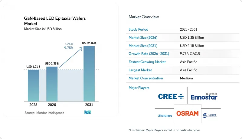
Demand is rising as metal-organic chemical vapor deposition platforms mature, mini-LED and micro-LED display adoption accelerates, and electric-vehicle headlamp content climbs. Suppliers are shifting capacity from commodity general-lighting wafers toward high-value optoelectronic, sensing and automotive substrates that carry tighter wavelength-uniformity and defect specifications. Equipment makers are unlocking cost advantages on 200 mm and 300 mm formats, while vertically integrated Asia-Pacific players leverage upstream crystal-growth control and downstream packaging to compress development cycles.
Global GaN-Based LED Epitaxial Wafers Market Trends and Insights
Rapid Penetration of Mini and Micro-LED Displays
Display manufacturers are accelerating mini-LED and micro-LED programs to overcome OLED burn-in limitations and deliver higher peak brightness, driving demand for wafers with sub-5 nm wavelength uniformity on 200 mm and 300 mm diameters. Ennostar announced a 200 mm GaN-on-Si initiative with ALLOS Semiconductors targeting wearable screens exceeding 2,000 PPI. Apple has invested USD 334 million with AU Optronics and Epistar in Hsinchu Science Park to secure vertically integrated epitaxial supply for future wearable displays. Automotive cross-pollination is evident in ams OSRAM's EVIYOS HD25 module, integrated into the NIO ET9, which packs 25,600 micro-LED pixels and requires display-grade epitaxy for 500 m projection.
Expansion of Electric-Vehicle Headlamp Production
Electric-vehicle makers specify adaptive headlamps topping 10,000 pixels, mandating low-defect, high-brightness wafers that survive stringent AEC-Q cycles. The EVIYOS HD25 raises projection distance from 400 m to 500 m and boosts low-beam luminance by 50% for mid-speed driving, illustrating the wafer performance leap required. Premium EVs now incorporate more than 100 LED packages, each drawing epitaxial material that must maintain chromatic stability across wide temperature swings.
Capital-Intensive MOCVD Tool Upgrades
State-of-the-art 300 mm GaN reactors cost more than USD 5 million apiece, while full production clusters require eight to ten tools plus in-situ metrology and robotics. Veeco expects its Propel300 revenues to hit USD 80 million in 2026, implying only a handful of fabs can currently absorb such capital. Smaller epitaxial-wafer suppliers face a strategic dilemma: legacy 150-millimeter and 200-millimeter MOCVD tools are fully depreciated and can produce wafers at competitive cash costs, but these platforms cannot match the die-per-wafer economics of 300-millimeter formats, risking margin compression as large foundries scale.
Other drivers and restraints analyzed in the detailed report include:
- Government Subsidies for Solid-State Lighting Programs
- Emerging Use of Free-Standing GaN Substrates
- Supply Volatility of High-Purity Sapphire Boules
For complete list of drivers and restraints, kindly check the Table Of Contents.
Segment Analysis
Wafers up to 150 mm commanded 68.71% of 2025 revenue, reflecting legacy MOCVD fleets built during the general-lighting boom. The GaN-based LED epitaxial wafers market size for 300 mm substrates is projected to expand at a 10.89% CAGR as foundries chase die-count economies and compatibility with silicon CMOS lines. Mid-scale 200 mm formats bridge current display backlight demand while 300 mm ecosystems mature, exemplified by the Ennostar-ALLOS project aimed at micro-LED wearables. The 300 mm transition is most acute in power and RF, where co-integrating GaN and CMOS drivers on one wafer trims module footprint and cost. However, larger diameters exacerbate thermal non-uniformity, forcing advanced susceptor designs and real-time pyrometry.
Cost dynamics ripple upstream: substrate vendors must now supply 300 mm sapphire and silicon wafers meeting tighter flatness and surface-roughness specs. ROHM Semiconductor and TSMC's February 2026 alliance leverages existing 300 mm clean-room assets to co-develop GaN power devices, highlighting the pull of shared infrastructure. Yet capital intensity and lengthy automotive qualifications mean widespread 300 mm adoption will remain limited to well-capitalized fabs through the forecast period.
Optoelectronics maintained 44.28% revenue leadership in 2025, anchored by mini-LED backlights and general illumination, but sensors are expected to post a 10.97% CAGR as vertical-cavity surface-emitting lasers and LiDAR sources proliferate. The GaN-based LED epitaxial wafers market share for discrete power devices is rising more gradually, constrained by cost-sensitive charger applications prioritizing price over defect density.
The sensors segment's rapid growth reflects the convergence of automotive safety regulations mandating advanced driver-assistance systems and consumer demand for facial recognition and augmented-reality features in smartphones and wearables. The micro segment, encompassing micro-electromechanical systems and micro-scale photonic devices, is emerging as a wildcard; while current volumes are limited, the potential for GaN-based micro-resonators and photonic integrated circuits to enable chip-scale light detection and ranging could create a new demand vector for ultra-low-defect epitaxial wafers. While optoelectronics will likely remain dominant, its lead narrows as sensing demand accelerates.
The GaN-Based LED Epitaxial Wafers Market Report is Segmented by Wafer Diameter (Up To 150 Mm, 200 Mm, and More), Semiconductor Device Type (Logic, Memory, Analog, Discrete, Optoelectronics, and More), Wafer Type (Prime, Polished, Epitaxial, Silicon-On-Insulator, Specialty Silicon, and More), End-User (Consumer Electronics, Mobile and Smartphones, and More), and Geography. The Market Forecasts are Provided in Terms of Value (USD).
Geography Analysis
Asia-Pacific held 56.27% of 2025 revenue and is projected to climb at a 10.73% CAGR, underpinned by Taiwan's vertically integrated clusters and China's subsidized capacity expansions. Taiwanese firms such as Epistar, Lextar and Ennostar work in close proximity to panel assemblers, accelerating feedback loops vital for micro-LED production. Chinese champion Sanan Optoelectronics is scaling aggressively, aided by state incentives and its pending Lumileds acquisition that unlocks Western automotive channels.
North America and Europe contribute a smaller yet strategic portion of demand. United States DOE funding offsets early-stage risk for novel epitaxial routes, while European automakers require AEC-Q qualified wafers for adaptive headlights, giving local suppliers premium pricing headroom. Technology flows bidirectionally, as European LED innovations like ams OSRAM's EVIYOS find application in Chinese EVs, underlining the global integration of supply chains.
The Rest of World region, including South America, the Middle East and Africa, remains nascent, relying on imported LED modules for illumination and signage. Nevertheless, government programs aimed at indigenous semiconductor capacity could lift regional wafer demand over the long term, especially if initiatives prioritize compound-semiconductor devices for renewable-energy or telecom-infrastructure goals.
- Nichia Corporation
- Cree Inc.
- Ennostar Corporation
- Osram Opto Semiconductors GmbH
- Sanan Optoelectronics Co., Ltd.
- Seoul Semiconductor Co., Ltd.
- Lumileds Holding B.V.
- Sumitomo Electric Industries, Ltd.
- AIXTRON SE
- Veeco Instruments Inc.
- Coherent Corp.
- Kyma Technologies
- Plessey Semiconductors Ltd.
- QROMIS Inc.
- Optowide Technologies Co., Ltd.
- IntelliEPI Inc.
- AdvanceNano
- IQE Plc
- Lextar Electronics Corporation
Additional Benefits:
- The market estimate (ME) sheet in Excel format
- 3 months of analyst support
TABLE OF CONTENTS
1 INTRODUCTION
- 1.1 Study Assumptions and Market Definition
- 1.2 Scope of the Study
2 RESEARCH METHODOLOGY
3 EXECUTIVE SUMMARY
4 MARKET LANDSCAPE
- 4.1 Market Overview
- 4.2 Market Drivers
- 4.2.1 Government Subsidies for Solid-State Lighting Programs
- 4.2.2 Rapid Penetration of Mini and Micro-LED Displays
- 4.2.3 Expansion of Electric-Vehicle Headlamp Production
- 4.2.4 Emerging Use of Free-Standing GaN Substrates to Cut Defects
- 4.2.5 Shift Toward Au-Free, Cu-Based Metallization to Reduce Cost
- 4.2.6 On-site Regrowth Techniques Enabling Vertical LEDs
- 4.3 Market Restraints
- 4.3.1 Capital-Intensive MOCVD Tool Upgrades
- 4.3.2 Supply Volatility of High-Purity Sapphire Boules
- 4.3.3 Thermal Management Challenges on 300 mm Platforms
- 4.3.4 IP Fragmentation Around Patterned Sapphire Substrates
- 4.4 Industry Analysis
- 4.5 Impact of Macroeconomic Factors
- 4.6 Porter's Five Forces Analysis
- 4.6.1 Bargaining Power of Suppliers
- 4.6.2 Bargaining Power of Buyers
- 4.6.3 Threat of New Entrants
- 4.6.4 Threat of Substitutes
- 4.6.5 Intensity of Competitive Rivalry
5 MARKET SIZE AND GROWTH FORECASTS (VALUE)
- 5.1 By Wafer Diameter
- 5.1.1 Up to 150 mm
- 5.1.2 200 mm
- 5.1.3 300 mm
- 5.2 By Semiconductor Device Type
- 5.2.1 Logic
- 5.2.2 Memory
- 5.2.3 Analog
- 5.2.4 Discrete
- 5.2.5 Optoelectronics
- 5.2.6 Sensors
- 5.2.7 Micro
- 5.3 By Wafer Type
- 5.3.1 Prime
- 5.3.2 Polished
- 5.3.3 Epitaxial
- 5.3.4 Silicon-on-Insulator (SOI)
- 5.3.5 Specialty Silicon (High-Resistivity)
- 5.3.6 Power
- 5.3.7 Sensor-Grade
- 5.4 By End-user
- 5.4.1 Consumer Electronics
- 5.4.2 Mobile and Smartphones
- 5.4.3 PCs and Servers
- 5.4.4 Industrial
- 5.4.5 Telecommunications
- 5.4.6 Automotive
- 5.4.7 Other End-user Applications
- 5.5 By Geography
- 5.5.1 North America
- 5.5.2 Europe
- 5.5.3 Asia-Pacific
- 5.5.4 Rest of the World
6 COMPETITIVE LANDSCAPE
- 6.1 Market Concentration
- 6.2 Strategic Moves
- 6.3 Market Share Analysis
- 6.4 Company Profiles (includes Global Level Overview, Market Level Overview, Core Segments, Financials as available, Strategic Information, Market Rank/Share, Products and Services, Recent Developments)
- 6.4.1 Nichia Corporation
- 6.4.2 Cree Inc.
- 6.4.3 Ennostar Corporation
- 6.4.4 Osram Opto Semiconductors GmbH
- 6.4.5 Sanan Optoelectronics Co., Ltd.
- 6.4.6 Seoul Semiconductor Co., Ltd.
- 6.4.7 Lumileds Holding B.V.
- 6.4.8 Sumitomo Electric Industries, Ltd.
- 6.4.9 AIXTRON SE
- 6.4.10 Veeco Instruments Inc.
- 6.4.11 Coherent Corp.
- 6.4.12 Kyma Technologies
- 6.4.13 Plessey Semiconductors Ltd.
- 6.4.14 QROMIS Inc.
- 6.4.15 Optowide Technologies Co., Ltd.
- 6.4.16 IntelliEPI Inc.
- 6.4.17 AdvanceNano
- 6.4.18 IQE Plc
- 6.4.19 Lextar Electronics Corporation
7 MARKET OPPORTUNITIES AND FUTURE OUTLOOK
- 7.1 White-space and Unmet-need Assessment

