
|
시장보고서
상품코드
2063848
아시아태평양의 LED 에피텍셜 웨이퍼 : 시장 점유율 분석, 업계 동향 및 통계, 성장 예측(2026-2031년)Asia-Pacific LED Epitaxial Wafer - Market Share Analysis, Industry Trends & Statistics, Growth Forecasts (2026 - 2031) |
||||||
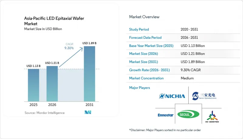
Mordor Intelligence에 의하면, 아시아태평양의 LED 에피텍셜 웨이퍼 시장 규모는 2025년 11억 3,000만 달러로 평가되었습니다. 2026년에는 12억 1,000만 달러로 확대되어 2026년부터 2031년에 걸쳐 CAGR 9.3%로 성장을 지속하여, 2031년까지 18억 9,000만 달러에 이를 것으로 예측됩니다.
본 보고서는 소재 시스템(GaN계 에피택셜 웨이퍼, AlInGaP계 에피택셜 웨이퍼 등), 기판 유형(사파이어, 실리콘, 실리콘 카바이드(SiC), 갈륨 비소(GaAs)), 웨이퍼 직경(100mm 이하, 150mm, 200mm 이상), 용도(일반 조명, 자동차용 조명, 디스플레이 및 백라이트 등)에 따라 분류되어 있습니다. 시장 전망은 금액(달러) 기준으로 제시되어 있습니다.
아시아태평양의 LED 에피택셜 웨이퍼 시장 동향 및 인사이트
마이크로 LED 및 미니 LED의 활용 분야 확대
액티브 매트릭스 방식의 Mini-LED TV는 2026년에 전 세계 출하 대수의 10% 점유율에 도달할 것으로 예상되며, HDR 환경에서 발생하는 색상 편차를 방지하기 위해 웨이퍼 제조업체는 6인치 기판 전체에서 ±2nm 미만의 파장 비닝을 실현해야 합니다. Tier 1 자동차 제조업체들은 고급 계기판에 미니 LED 백라이트를 탑재하기 시작하면서, 결함이 적은 GaN 에피택시 수요를 견인하고 있습니다. 삼성디스플레이와 LG디스플레이는 웨어러블 기기용 마이크로 LED 시범 생산 라인에 투자하고 있습니다. 이 분야에서는 패널 1제곱미터당 기존 LED의 최대 10배에 달하는 웨이퍼 면적을 사용하기 때문에 필요한 수량이 급격히 증가합니다. 샤오미의 163인치 프로토타입은 양산 시 불량률을 1ppm 미만으로 억제할 수 있다는 전제 하에 확장성을 입증했습니다. 이러한 프로젝트들은 성능 편차가 발생할 때마다 후속 전사 공정에서 수정이 필요하기 때문에 평균 판매 가격을 상승시키는 요인이 됩니다.
고휘도 자동차용 헤드램프 수요 증가
UNECE 및 개정된 중국 GB 규정에 따라, 눈부심을 억제하면서도 3,000루멘을 초과하는 광속을 가진 적응형 주행 빔 모듈이 현재 허용되고 있습니다. 니치아 화학공업의 DominoPLS 디바이스는 모듈당 16개의 주소 지정 가능한 부문을 통합하고 있으며, UNECE 및 GB의 광도 시험 요건을 모두 충족합니다. 인도의 AIS-199 규격 초안은 세계 표준을 따르고 있으며, 매트릭스 헤드램프에 새로운 지역적 길을 열어주고 있습니다. 각 자동차 OEM 업체들은 피크 파장을 450 nm±5 nm, 전위 밀도를 1×10^8 cm-2 미만으로 규정하고 있으며, 에피택셜 제조업체들에게 고도의 버퍼 스택을 갖춘 더 큰 크기의 사파이어 또는 SiC 기판으로의 전환을 요구하고 있습니다.
사파이어 기판 공급망의 변동
2026년까지 중국은 전 세계 사파이어 잉곳 공급량의 40% 이상을 차지할 것으로 예상되지만, 수출 규제나 물류 차질이 발생하면 그 영향은 즉시 아시아태평양의 전체 팹으로 파급될 것입니다. 스마트폰용 카메라 커버 수요가 디스플레이 수요의 정점과 겹치는 시기에는 리드타임이 길어지며, 4인치 웨이퍼 가격은 장당 15-25달러 사이에서 변동합니다. 인도의 PLI(생산 연계형 인센티브) 규정에 따르면 3년 이내에 기판의 현지 조달률을 25%로 달성해야 하지만, 국내에 잉곳 생산 업체가 없기 때문에 팹은 수년에 걸친 수입 계약을 체결할 수밖에 없으며, 그 결과 보조금의 혜택이 줄어들게 됩니다.
부문별 분석
GaN 웨이퍼는 일반 조명, 자동차, 디스플레이용 백라이트 시장을 배경으로 2025년 출하량의 68.40%를 차지했습니다. 지자체들의 무수은 UV-C 살균 기술 도입에 따라, 아시아태평양의 AlGaN용 LED 에피택셜 웨이퍼 시장 규모는 2031년까지 연평균 성장률(CAGR) 12.87%로 확대될 것으로 전망됩니다. 니치아 화학공업의 280 nm 소자는 7.4%의 월플러그 효율을 달성하여 상업적 실현 가능성을 입증했을 뿐만 아니라, 수도 유틸리티자들의 조달을 촉진했습니다.
현재 가격은 전구용으로서 범용화된 GaN과, 파장 균일성 ±2 nm 및 결함 밀도 1 cm² 미만의 사양을 충족하는 프리미엄 GaN 또는 AlGaN 웨이퍼 사이에서 양극화되어 있습니다. AlGaN에서 알루미늄 함유율이 높아지면 균열 발생 위험이 커지기 때문에 각 제조업체들은 알루미늄 질화물 버퍼층이나 펄스식 횡방향 성장법을 실험하고 있습니다. 따라서 소재 선정은 처리량, 에피택셜 응력, 그리고 특히 의료용 멸균 분야에서 발생하는 새로운 자외선 수요와의 균형에 달려 있습니다.
사파이어는 격자 정합성이 우수하고 반응로의 화학 공정이 성숙해져 있어, 2025년에는 55.67%의 시장 점유율을 차지했습니다. 실리콘 기판 시장은 연평균 성장률(CAGR) 13.58%로 성장하고 있으며, 200mm 웨이퍼공급 안정성과 반도체 등급의 측정 기술을 활용하여 다이당 비용을 절감하고 있습니다. Innoscience사는 그라데이션 AlGaN 버퍼층을 도입하고 실시간 응력 모니터링을 실시한 후, 8인치 GaN-on-silicon 웨이퍼에서 97%의 수율을 달성했습니다.
실리콘 카바이드는 비용이 3-5배 더 비싸기 때문에 여전히 틈새 시장 소재로 남아 있지만, 대전류 LED에 탁월한 열전도율을 제공합니다. 갈륨 비소는 적색·호박색의 AlInGaP에 사용되지만, 직경에 제한이 있습니다. 따라서 아시아태평양의 LED 에피택셜 웨이퍼 시장 점유율 균형은 디스플레이 및 자동차 업계의 고객들이 비용을 우선시할지, 아니면 열적 여유를 우선시할지에 따라 결정됩니다.
추가적인 장점 :
- Excel 형식 시장 예측(ME) 시트
- 3개월간의 애널리스트 지원
자주 묻는 질문
목차
제1장 서론
제2장 조사 방법
제3장 주요 요약
제4장 시장 구도
제5장 시장 규모 및 성장 예측
제6장 경쟁 구도
제7장 시장 기회 및 향후 전망
KTHAccording to Mordor Intelligence, the asia-Pacific lED epitaxial wafer market size is expected to grow from USD 1.13 billion in 2025 to USD 1.21 billion in 2026 and is forecast to reach USD 1.89 billion by 2031 at 9.3% CAGR over 2026-2031.

This report is Segmented by Material System (GaN-Based Epitaxial Wafers, Alingap Epitaxial Wafers, and More), Substrate Type (Sapphire, Silicon, Silicon Carbide (SiC), Gallium Arsenide (GaAs)), Wafer Diameter (Up To 100 Mm, 150 Mm, 200 Mm and Above), and Application (General Lighting, Automotive Lighting, Displays and Backlighting and More). The Market Forecasts are Provided in Terms of Value (USD).
Asia-Pacific LED Epitaxial Wafer Market Trends and Insights
Expansion of Micro-LED and Mini-LED Applications
Active-matrix Mini-LED televisions reached 10% penetration in global shipments in 2026, compelling wafer makers to achieve wavelength binning tighter than +-2 nm across 6-inch substrates to avoid color-shift artifacts under HDR conditions. Tier-1 automakers have begun equipping high-end instrument clusters with Mini-LED backlights, reinforcing demand for low-defect GaN epitaxy. Samsung Display and LG Display are funding Micro-LED pilot lines for wearables, where each square meter of panel uses up to ten-times more wafer area than conventional LEDs, multiplying volume requirements. Xiaomi's 163-inch prototype validated scalability, contingent on mass-transfer yields below one-ppm defect rates. These projects elevate average selling prices because every performance drift incurs rework in downstream transfer processes.
Rising Demand for High-Brightness Automotive Headlamps
UNECE and updated Chinese GB regulations now allow adaptive-driving-beam modules that exceed 3 000 lumens while controlling glare. Nichia's DominoPLS devices integrate 16 addressable segments per module, meeting both UNECE and GB photometric test requirements. India's draft AIS-199 standard aligns with global norms, opening a new regional route for matrix headlamps. Automotive OEMs stipulate peak wavelengths at 450 nm +-5 nm and dislocation densities below 1 X 10^8 cm-2, pushing epitaxial houses toward larger sapphire or SiC substrates with advanced buffer stacks.
Supply Chain Volatility of Sapphire Substrates
China will supply more than 40% of global sapphire ingots by 2026, but any export controls or logistical disruptions will instantly reverberate across Asia-Pacific fabs. Lead times stretch when smartphone camera-cover demand overlaps display peaks, sending 4-inch wafer prices swinging between USD 15 and USD 25 apiece. India's PLI rules require 25% local substrate value within three years, yet no domestic ingot producer exists, forcing fabs to lock multi-year import contracts that dilute subsidy benefits.
Other drivers and restraints analyzed in the detailed report include:
- Rapid Urban Smart-Lighting Initiatives
- Government Subsidies for Regional Semiconductor Manufacturing
- High Capital Expenditure for MOCVD Tools
For complete list of drivers and restraints, kindly check the Table Of Contents.
Segment Analysis
GaN wafers dominated 68.40% of shipments in 2025 on the back of general lighting, automotive, and display backlighting. The Asia-Pacific LED Epitaxial Wafer market size for AlGaN is projected to expand at 12.87% CAGR through 2031 as municipalities adopt mercury-free UV-C disinfection. Nichia's 280 nm devices, delivering 7.4% wall-plug efficiency, validated commercial viability and sparked procurement from water-utility operators.
Pricing now bifurcates between commoditized GaN for bulbs and premium GaN or AlGaN wafers meeting +-2 nm wavelength uniformity and sub-1 cm-2 defect specs. Elevated aluminum fractions in AlGaN raise cracking risks, so producers are experimenting with aluminum-nitride buffer layers and pulsed lateral overgrowth. Material selection thus hinges on balancing throughput, epitaxial stress, and emerging UV demand, especially for healthcare sterilization.
Sapphire held 55.67% share in 2025 because of favorable lattice matching and mature reactor chemistries. Silicon substrates, growing at a 13.58% CAGR, leverage 200 mm wafer availability and semiconductor-grade metrology to reduce the cost per die. Innoscience demonstrated 97% yield on 8-inch GaN-on-silicon wafers after implementing graded AlGaN buffers and real-time stress monitoring.
Silicon carbide remains a niche due to a 3-5X cost premium, yet offers unmatched thermal conductivity for high-current LEDs. Gallium-arsenide serves red-amber AlInGaP but is diameter-limited. The Asia-Pacific LED Epitaxial Wafer market share balance, therefore, depends on whether display and automotive clients prioritize cost or thermal headroom.
List of Companies Covered in this Report:
- Nichia Corporation
- Epistar Corporation
- Sanan Optoelectronics Co., Ltd.
- Osram Opto Semiconductors GmbH
- Seoul Semiconductor Co., Ltd.
- Wolfspeed, Inc.
- HC Semitek Corporation
- Genesis Photonics Inc.
- Opto Tech Corporation
- Bridgelux, Inc.
- Lumileds Holding B.V.
- Lextar Electronics Corporation
- Showa Denko K.K.
- Unistars Corporation
- Everlight Electronics Co., Ltd.
- Tyntek Corporation
- Epileds Technologies Inc.
- Focus Lightings Tech Co., Ltd.
- Sino-American Silicon Products Inc.
Additional Benefits:
- The market estimate (ME) sheet in Excel format
- 3 months of analyst support
TABLE OF CONTENTS
1 INTRODUCTION
- 1.1 Study Assumptions and Market Definition
- 1.2 Scope of the Study
2 RESEARCH METHODOLOGY
3 EXECUTIVE SUMMARY
4 MARKET LANDSCAPE
- 4.1 Market Overview
- 4.2 Market Drivers
- 4.2.1 Government Subsidies for Regional Semiconductor Manufacturing
- 4.2.2 Expansion of Micro-LED and Mini-LED Applications
- 4.2.3 Rising Demand for High-Brightness Automotive Headlamps
- 4.2.4 Rapid Urban Smart-Lighting Initiatives
- 4.2.5 Advancements in GaN-on-SiC Wafer Yields
- 4.2.6 Growing Investments in UV-C LED Sterilization Systems
- 4.3 Market Restraints
- 4.3.1 High Capital Expenditure for MOCVD Tools
- 4.3.2 Supply Chain Volatility of Sapphire Substrates
- 4.3.3 Thermal Mismatch Challenges in Large-Diameter Silicon Wafers
- 4.3.4 Intellectual-Property (IP) Licensing Barriers for Start-ups
- 4.4 Industry Value Chain Analysis
- 4.5 Impact of Macroeconomic Factors on the Market
- 4.6 Regulatory Landscape
- 4.7 Technological Outlook
- 4.8 Porter's Five Forces Analysis
- 4.8.1 Threat of New Entrants
- 4.8.2 Bargaining Power of Suppliers
- 4.8.3 Bargaining Power of Buyers
- 4.8.4 Threat of Substitutes
- 4.8.5 Industry Rivalry
5 MARKET SIZE AND GROWTH FORECASTS (VALUE)
- 5.1 By Material System
- 5.1.1 GaN-based Epitaxial Wafers
- 5.1.2 AlInGaP Epitaxial Wafers
- 5.1.3 AlGaN Epitaxial Wafers
- 5.2 By Substrate Type
- 5.2.1 Sapphire
- 5.2.2 Silicon
- 5.2.3 Silicon Carbide (SiC)
- 5.2.4 Gallium Arsenide (GaAs)
- 5.3 By Wafer Diameter
- 5.3.1 Upto 100 mm
- 5.3.2 150 mm
- 5.3.3 200 mm and Above
- 5.4 By Application
- 5.4.1 General Lighting
- 5.4.2 Automotive Lighting
- 5.4.3 Displays and Backlighting
- 5.4.4 UV Sterilization
- 5.4.5 Industrial and Specialty Lighting
- 5.5 By Country
- 5.5.1 China
- 5.5.2 India
- 5.5.3 Japan
- 5.5.4 South Korea
- 5.5.5 Rest of the Asia-Pacific
6 COMPETITIVE LANDSCAPE
- 6.1 Market Concentration
- 6.2 Strategic Moves
- 6.3 Vendor Market Positioning
- 6.4 Company Profiles (includes Global Level Overview, Market Level Overview, Core Segments, Financials as available, Strategic Information, Market Rank/Share, Products and Services, Recent Developments)
- 6.4.1 Nichia Corporation
- 6.4.2 Epistar Corporation
- 6.4.3 Sanan Optoelectronics Co., Ltd.
- 6.4.4 Osram Opto Semiconductors GmbH
- 6.4.5 Seoul Semiconductor Co., Ltd.
- 6.4.6 Wolfspeed, Inc.
- 6.4.7 HC Semitek Corporation
- 6.4.8 Genesis Photonics Inc.
- 6.4.9 Opto Tech Corporation
- 6.4.10 Bridgelux, Inc.
- 6.4.11 Lumileds Holding B.V.
- 6.4.12 Lextar Electronics Corporation
- 6.4.13 Showa Denko K.K.
- 6.4.14 Unistars Corporation
- 6.4.15 Everlight Electronics Co., Ltd.
- 6.4.16 Tyntek Corporation
- 6.4.17 Epileds Technologies Inc.
- 6.4.18 Focus Lightings Tech Co., Ltd.
- 6.4.19 Sino-American Silicon Products Inc.
7 MARKET OPPORTUNITIES AND FUTURE OUTLOOK
- 7.1 White-Space and Unmet-Need Assessment
