

|
시장보고서
상품코드
2099437
GPU 칩렛 패키징 시장 : 점유율 분석, 업계 동향 및 통계, 성장 예측(2026-2031년)GPU Chiplet Packaging - Market Share Analysis, Industry Trends & Statistics, Growth Forecasts (2026 - 2031) |
||||||
 Mordor Intelligence
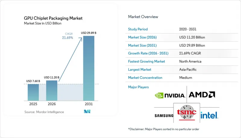
Mordor Intelligence에 의하면, GPU 칩렛 패키징 시장 규모는 2025년 76억 달러에서 2026년에는 112억 달러로 확대되어 2031년까지 298억 9,000만 달러에 이를 것으로 예상되고 있어 2026년부터 2031년까지 CAGR 21.69%로 성장할 전망입니다.
본 보고서는 GPU 플랫폼(데이터센터 및 AI용 GPU 등), 패키징 기술(2.5D 인터포저 및 브리지 기반 패키징 등), 치플릿의 기능(GPU 연산용 치플릿 등), 용도(AI 훈련 및 추론, 클라우드 컴퓨팅 등), 최종 사용자(하이퍼스케일러 및 클라우드 제공업체 등), 지역별로 분류되어 있습니다. 시장 전망은 금액(달러) 기준으로 제시되어 있습니다.
세계 GPU 칩렛 패키징 시장 동향 및 인사이트
HBM 탑재 패키지에 대한 AI GPU 수요 증가
하이퍼스케일러의 AI 인프라 투자는 GPU 칩렛 패키징 시장에 있어 여전히 가장 명확한 단기 수요 견인 요인으로 작용하고 있습니다. NVIDIA의 데이터센터 부문은 2026년 4월에 종료된 2027 회계연도 1분기에 752억 달러의 매출을 기록했으며, 이는 전년 동기 대비 92% 증가한 수치입니다. 또한, 2027 회계연도 2분기 실적 전망치는 910억 달러로 설정되었습니다. 이 초안에서는 제품의 양산 확대가 패키지의 복잡성과 직접적으로 연결되어 있다고 지적하고 있습니다. 이는 각 Blackwell B200 패키지가 CoWoS-L 기판 위에 2개의 연산 다이와 8개의 HBM3E 스택을 결합하고 있기 때문입니다. 이러한 구성으로 인해 AI GPU 신규 주문 1건당 첨단 패키징 라인, 첨단 기판 및 고밀도 메모리 통합에 대한 직접적인 수요가 발생합니다. 그 결과, GPU 칩렛 패키징 시장은 더 이상 광범위한 반도체 사이클에 의해 주로 형성되는 것이 아니라, 초대형 가속기의 도입 시기에 따라 좌우되게 되었습니다. 이는 또한 패키징 역량이 단순한 일상적인 백엔드 제조 공정이 아니라 전략적 병목 현상이 된 이유도 설명해 줍니다.
데이터센터 성능 확장을 위한 이종 통합
단순한 공정 미세화만으로는 최첨단 가속기에 대해 시스템 수준에서 충분한 성능 향상을 가져올 수 없게 되었기 때문에 이종 통합이 핵심적인 성능 향상 수단이 되고 있습니다. 인텔에 따르면, Foveros Direct 3D는 구리 대 구리 직접 본딩을 통해 10µm 미만의 상호 연결 피치를 실현하며, 기존의 마이크로 범프 방식에 비해 최대 10배의 상호 연결 밀도를 제공할 수 있다고 합니다. 이러한 수준의 밀도는 연산, 메모리, I/O 기능이 극히 좁은 물리적 거리 내에서 작동해야 하는 경우에 요구되는 다이 수직 적층 레이아웃을 지원합니다. 이 아키텍처의 논리는 플래그십 GPU에 그치지 않고, 하이퍼스케일러 팀이 설계하는 맞춤형 AI 추론용 실리콘 프로그램으로도 확대되고 있습니다. 이로 인해 GPU 칩렛 패키징 시장의 잠재적 수요 기반은 표준 GPU 벤더의 로드맵을 넘어 확대될 것입니다. 또한 설계, 열, 조립에 대한 제약을 동시에 고려하여 대응할 수 있는 패키징 팀의 중요성도 높아지고 있습니다.
높은 패키징 비용과 제한된 대량 생산 능력
패키징 비용의 높음은 여전히 최첨단 구성이 최고 부가가치의 컴퓨팅 프로그램에 한정되는 요인이 되고 있습니다. 초안에 따르면, 현세대 AI GPU용 CoWoS-L 패키징은 더 단순한 CoWoS-S 설계에 비해 추가적인 로컬 실리콘 브리지 요소, 더 많은 마이크로 범프 수, 그리고 초기 단계의 조립 수율 저하를 수반합니다. 이러한 비용 차이는 중요한 의미를 지닙니다. 왜냐하면 시장의 성장을 주도하고 있는 고객들이 바로 이용 가능한 인증 생산 능력의 대부분을 확보하고 있기 때문입니다. 공급 문제는 조립 공정에만 국한되지 않습니다. 상용 생산을 원활하게 확대하기 위해서는 기판, 특수 소재, 본딩 장비 모두가 연계되어 규모를 확대해야 하기 때문입니다. 또한, 각 새로운 패키지의 경우, 수익이 확대되기 전에 GPU, HBM, 기판 각 공급업체 간에 조율된 인증 절차를 거쳐야 합니다. 그 결과, GPU 칩렛 패키징 시장은 수요 전망은 밝지만, 공급 체계 구축이 뒤처지고 있는 구조적인 불일치에 직면해 있습니다.
부문 분석
2025년 시점에서 데이터센터 및 AI용 GPU는 GPU 칩렛 패키징 시장 점유율의 86.11%를 차지하고 있으며, 2031년까지 연평균 성장률(CAGR) 23.21%로 확대될 것으로 예측됩니다. 이러한 집중 경향은 하이퍼스케일러와 기업의 AI 프로그램이 사상 최대 판매 대수를 기록한 디바이스가 아닌, 패키징 부하가 가장 높은 디바이스를 발주하고 있다는 사실을 반영합니다. 이러한 플랫폼에는 CoWoS-L, 첨단 유기 기판 플립칩 또는 3D 통합 기법이 필요하며, 이들은 표준 클라이언트용 그래픽스 제품보다 칩당 패키징 가치가 훨씬 더 높습니다. NVIDIA의 2027 회계연도 1분기 데이터센터 부문 매출 752억 달러는 이 부문을 뒷받침하는 수요의 강세를 보여주는 올해의 지표입니다. 따라서 GPU 칩렛 패키징 시장은 최대 메모리 대역폭 수요와 최대 패키징 복잡성을 모두 갖춘 플랫폼 등급에 의해 주도되고 있습니다.
HPC GPU는 본 초안에서 두 번째로 큰 규모를 차지하는 플랫폼을 형성하고 있으며, 여전히 고성능 2.5D 패키징이 필요한 과학 계산, 기후 모델링, 국방 분야의 워크로드를 처리하고 있습니다. 출하 대수는 AI 가속기 등급보다 적지만, 성능과 신뢰성에 대한 요구 사항은 여전히 까다롭습니다. 전문가용 및 워크스테이션용 GPU는 중위권에 위치하며, 이 부문에서는 풀 실리콘 인터포저 통합보다 첨단 유기 기판 솔루션이 더 일반적입니다. 클라이언트 및 게이밍용 GPU는 여전히 큰 출하량을 차지하고 있지만, 패키지 구조의 밀도가 낮고 메모리 사용량도 적기 때문에 칩당 고급 패키징을 통한 수익은 낮은 임베디드니다. AI 가속기가 더 큰 패키지 실적와 더 많은 HBM 스택 수로 전환됨에 따라, 출하량과 패키징 가치 간의 이러한 격차는 확대되고 있습니다. 이러한 격차의 확대는 GPU 칩렛 패키징 시장에서 데이터센터용 GPU의 프리미엄 지위를 더욱 공고히 하고 있습니다.
2025년에는 2.5D 인터포저 및 브리지 기반 패키징이 GPU 칩렛 패키징 시장 규모의 68.33%를 차지했으나, 3D 적층 및 하이브리드 본딩 패키징은 2031년까지 연평균 성장률(CAGR) 23.62%를 나타낼 것으로 예측됩니다. 2.5D 형식이 현재 주도적인 위치를 차지하고 있는 것은 시중에 판매되고 있는 현행 AI 가속기에서 그 제조 체제가 확립되어 있음을 반영합니다. TSMC의 CoWoS 제품군과 인텔의 EMIB 플랫폼은 양산 공급 및 패키지의 신뢰성 측면에서 현재 고객들로부터 이미 신뢰를 얻고 있는 생산 기반을 구축하고 있습니다. 또한 인텔은 Foveros Direct 3D를 보다 정밀한 직접 본딩과 고밀도 수직 집적을 실현하는 차세대 로드맵으로 자리매김하고 있습니다. 이는 3D 기술의 전략적 중요성이 커지고 있음에도 불구하고, GPU 칩렛 패키징 시장은 여전히 2.5D 매출에 의해 지탱되고 있음을 의미합니다.
이 초안에 따르면, 향후 메모리 및 로직 설계에는 기존 마이크로 범프 공정으로는 대응할 수 없을 정도로 미세한 상호 연결 지오메트리가 필요하기 때문에 3D 적층 및 하이브리드 본딩 방식이 주목받고 있습니다. 팬아웃 및 RDL 기반 패키징은 실리콘 인터포저 방식과 같은 전체 비용 부담을 수반하지 않으면서도 고도의 집적화를 필요로 하는 고객에게 대안적인 경로를 제공합니다. 유기 기판 기반의 멀티 다이 패키징은 대역폭 밀도나 열 부하가 비교적 낮은 클라이언트용 GPU 및 엔트리 레벨 워크스테이션 용도에서 여전히 중요한 역할을 하고 있습니다. 또한, 고대역폭 메모리 인터페이스나 다이 간 연결은 더욱 엄격한 전기적·열적 제한 범위 내에서 인증을 받아야 하므로, 규격 준수도 점점 더 중요해지고 있습니다. 이에 따라 상업적 채택에 있어서는 단순히 참신함뿐만 아니라 공정의 성숙도가 핵심 요소가 됩니다. 그 결과, GPU 칩렛 패키징 시장은 단계적으로 변화할 전망이며, 양산 측면에서는 2.5D가 계속해서 주류를 이루는 한편, 3D는 우선 고부가가치 프로그램에서 확대될 것입니다.
지역별 분석
2025년, 아시아태평양은 GPU 칩렛 패키징 시장 점유율의 88.44%를 차지하고 있으며, 이는 해당 지역에 파운드리, OSAT, 기판 공급업체, 메모리 제조업체가 고도로 집중되어 있음을 반영합니다. 대만은 TSMC의 첨단 패키징 거점과 ASE Technology Holding의 반도체 조립·테스트 수탁(OSAT) 규모를 통해 이 생태계의 핵심 역할을 하고 있습니다. 대만의 강점은 생산 능력뿐만 아니라 패키징 소재, 기판, 엔지니어링 인력에 이르는 공급망의 근접성에도 있습니다. 한국은 HBM 메모리 분야의 리더십과 AI 가속기에 여전히 필수적인 관련 패키지 통합 능력을 통해 이 지역 내 입지를 공고히 하고 있습니다. 또한, 일본 현지 공급업체의 ABF 기판 생산이 더 광범위한 패키징 체인에서 중요한 병목 현상으로 작용하고 있기 때문에 일본 역시 전략적 중요성을 유지하고 있습니다.
북미는 2031년까지 연평균 성장률(CAGR) 23.42%를 나타낼 것으로 예측되며, GPU 칩렛 패키징 시장에서 가장 빠르게 성장하는 지역 클러스터가 될 전망입니다. 'CHIPS and Science Act'는 국내 제조 및 패키징을 위한 보다 견고한 투자 기반을 구축하며, 인용된 CRS 보고서에 따르면 민관 인센티브 총액은 467억 달러에 달할 전망입니다. 애머콜(Amcor)의 애리조나주 첨단 패키징 캠퍼스와 월드 파운드리(World Foundries)의 뉴욕 첨단 패키징 및 포토닉스 센터는 이러한 정책에 힘입어 거점을 확장한 가장 대표적인 사례입니다. 월드 파운드리(World Foundries)에 따르면, 이 회사의 뉴욕 센터는 2025년 1월에 개소했으며, 5억 7,500만 달러의 투자와 ‘CHIPS and Science Act’에 따른 7,500만 달러의 직접 지원을 받고 있습니다. 이 지역의 성장률이 견조한 것은 현재의 가동 능력 면에서 아시아태평양을 대체할 만큼 근접해 있기 때문이 아니라, 낮은 수준에서 출발했기 때문입니다.
유럽은 GPU 칩렛 패키징 시장에서 상업적 입지는 미미하지만, 3D 통합 및 이종 패키징 연구에서는 여전히 중요한 위치를 차지하고 있습니다. 이 지역의 중요성은 대규모 양산 실적이라기보다는 imec, 프라운호퍼 연구소, CEA-Leti 등의 연구 기관에서 이루어지는 연구 개발에 기인합니다. 남미, 중동 및 아프리카는 여전히 수요의 초기 단계에 있는 지역으로, 현재로서는 실질적인 최첨단 패키징 제조 거점이 존재하지 않습니다. 중동은 각국 정부의 AI 투자 프로그램을 통해 수요 거점으로 부상하고 있지만, 아프리카의 역할은 여전히 광범위한 데이터센터 건설과 수입된 가속기공급에 의존하고 있습니다.
기타 혜택:
- 엑셀 형식 시장 예측(ME) 시트
- 3개월간의 애널리스트 지원
자주 묻는 질문
목차
제1장 서론
제2장 조사 방법
제3장 주요 요약
제4장 시장 구도
제5장 시장 규모와 성장 예측
제6장 경쟁 구도
제7장 시장 기회와 향후 전망
JHS 26.08.05According to Mordor Intelligence, the GPU chiplet packaging market size is expected to increase from USD 7.60 billion in 2025 to USD 11.20 billion in 2026 and reach USD 29.89 billion by 2031, growing at a CAGR of 21.69% over 2026-2031.
This report is Segmented by GPU Platform (Data Center and AI GPUs, and More), Packaging Technology (2. 5D Interposer and Bridge-Based Packaging, and More), Chiplet Function (GPU Compute Chiplets, and More), Application (AI Training and Inference, Cloud Computing, and More), End User (Hyperscalers and Cloud Providers, and More), and Geography. The Market Forecasts are Provided in Terms of Value (USD).
Global GPU Chiplet Packaging Market Trends and Insights
Rising AI GPU Demand for HBM-Attached Packages
Hyperscaler AI infrastructure spending remains the clearest near-term demand driver for the GPU chiplet packaging market. NVIDIA's data center segment generated USD 75.2 billion in Q1 FY2027, the quarter ending April 2026, and this was 92% higher than the prior year, while Q2 FY2027 guidance was set at USD 91.0 billion. The draft links that product ramp directly to package complexity, because each Blackwell B200 package combines 2 compute dies with 8 HBM3E stacks on a CoWoS-L substrate. That configuration means each new AI GPU order translates into direct demand for advanced packaging lines, advanced substrates, and high-density memory integration. The result is that the GPU chiplet packaging market is no longer being shaped mainly by broad semiconductor cycles, but by the timing of very large accelerator deployments. This also explains why packaging capacity has become a strategic bottleneck rather than a routine back-end manufacturing step.
Heterogeneous Integration for Datacenter Performance Scaling
Heterogeneous integration has become a core performance lever because simple process shrinks no longer deliver enough system-level gain for leading accelerators. Intel stated that Foveros Direct 3D achieves sub-10 µm interconnect pitch through direct copper-to-copper bonding and can provide up to 10x finer interconnect density than conventional microbump approaches. That level of density supports the vertical die-stacking layouts needed when compute, memory, and I/O functions must operate within a very small physical distance. The same architectural logic is moving beyond flagship GPUs and into custom AI inference silicon programs designed by hyperscaler teams. This broadens the addressable volume base for the GPU chiplet packaging market beyond the standard GPU vendor roadmap. It also raises the importance of packaging teams that can work across design, thermal, and assembly constraints at the same time.
High Packaging Cost and Limited High-Volume Capacity
High package cost still limits the broad adoption of leading-edge configurations to the highest-value compute programs. The draft states that CoWoS-L packaging for current-generation AI GPUs requires added local silicon bridge elements, higher microbump counts, and lower early-stage assembly yields than simpler CoWoS-S designs. That cost difference matters because the same customers driving market growth are also reserving much of the available qualified capacity. The supply issue is wider than assembly alone, since substrates, specialty materials, and bonding tools all have to scale together for commercial output to increase smoothly. Each new package also needs coordinated qualification across GPU, HBM, and substrate suppliers before revenue can ramp. As a result, the GPU chiplet packaging market faces a structural mismatch between strong demand visibility and slower supply readiness.
Other drivers and restraints analyzed in the detailed report include:
- Yield Advantage of Smaller GPU Chiplets Versus Monolithic Dies
- Advanced Packaging Capacity Investments by Foundries and OSATs
- Thermal and Signal Integrity Complexity in Dense Interconnects
For complete list of drivers and restraints, kindly check the Table Of Contents.
Segment Analysis
Data Center and AI GPUs held 86.11% of GPU chiplet packaging market share in 2025 and are projected to expand at a 23.21% CAGR through 2031. This concentration reflects the fact that hyperscalers and enterprise AI programs are ordering the most packaging-intensive devices, not the highest historical unit-volume devices. These platforms require CoWoS-L, advanced organic substrate flip-chip, or 3D integration methods that carry far more packaging value per chip than standard client graphics products. NVIDIA's data center segment revenue of USD 75.2 billion in Q1 FY2027 provides a current-year anchor for the demand intensity behind this category. The GPU chiplet packaging market is therefore being led by the platform class that combines the greatest memory bandwidth needs with the greatest package complexity.
HPC GPUs form the second-largest platform in the draft and serve scientific computing, climate modeling, and defense workloads that still require highly capable 2.5D packaging. Their volumes are lower than the AI accelerator class, but their performance and reliability needs remain demanding. Professional and workstation GPUs sit in a middle tier, where advanced organic substrate solutions are more common than full silicon interposer integration. Client and gaming GPUs still represent a large unit base, but they produce less advanced packaging revenue per chip because their package structures are less dense and less memory intensive. This gap between unit volume and packaging value is widening as AI accelerators move to larger package footprints and higher HBM stack counts. That widening gap reinforces the premium position of data center GPUs within the GPU chiplet packaging market.
2.5D Interposer and Bridge-Based Packaging accounted for 68.33% of GPU chiplet packaging market size in 2025, while 3D Stacked and Hybrid-Bonded Packaging is forecast to grow at a 23.62% CAGR through 2031. The present leadership of 2.5D formats reflects proven manufacturing readiness across current AI accelerators in commercial shipment. TSMC's CoWoS family and Intel's EMIB platform established a production base that current customers already trust for volume delivery and package reliability. Intel also positioned Foveros Direct 3D as a next-stage path for tighter direct bonding and denser vertical integration. This means the GPU chiplet packaging market is still anchored by 2.5D revenue even as 3D technologies gain strategic importance.
The draft shows that 3D stacked and hybrid-bonded formats are gaining momentum because future memory and logic designs need much finer interconnect geometry than conventional microbump flows can support. Fan-Out and RDL-based packaging provides an alternative path for customers that need advanced integration without the full cost profile of silicon interposer approaches. Organic substrate-based multi-die packaging remains relevant for client GPU and entry workstation programs where bandwidth density and thermal load are more moderate. Standards compliance is also becoming more important because high-bandwidth memory interfaces and die-to-die connections have to qualify within tighter electrical and thermal limits. This puts process maturity, not just novelty, at the center of commercial adoption. As a result, the GPU chiplet packaging market is likely to move in stages, with 2.5D staying dominant in volume while 3D expands first in the highest-value programs.
Complete Report Scope:
- By GPU Platform
- Data Center and AI GPUs
- HPC GPUs
- Professional and Workstation GPUs
- Client and Gaming GPUs
- Other GPU Platforms
- By Packaging Technology
- 2.5D Interposer and Bridge-Based Packaging
- 3D Stacked and Hybrid-Bonded Packaging
- Fan-Out and RDL-Based Packaging
- Organic Substrate-Based Multi-Die Packaging
- Other Packaging Technologies
- By Chiplet Function
- GPU Compute Chiplets
- Memory Chiplets
- I/O and Base Die Chiplets
- Connectivity and Interface Chiplets
- Other Chiplets
- By Application
- AI Training and Inference
- High-Performance Computing
- Cloud Computing
- Professional Visualization
- Gaming and Consumer Graphics
- Other Applications
- By End User
- Hyperscalers and Cloud Providers
- Enterprise Data Centers
- Research and Government HPC Centers
- OEMs and System Integrators
- Other End Users
- By Geography
- North America
- United States
- Canada
- Mexico
- Europe
- Germany
- United Kingdom
- France
- Italy
- Rest of Europe
- Asia-Pacific
- China
- Japan
- South Korea
- India
- Southeast Asia
- Rest of Asia-Pacific
- South America
- Middle East
- Africa
- North America
Geography Analysis
Asia-Pacific held 88.44% of the GPU chiplet packaging market share in 2025, which reflects the region's deep concentration of foundries, OSATs, substrate suppliers, and memory producers. Taiwan anchors this ecosystem through TSMC's advanced packaging base and ASE Technology Holding's scale in outsourced semiconductor assembly and test. Taiwan's advantage is not only production capacity, but also supply chain proximity across packaging materials, substrates, and engineering talent. South Korea supports the regional position through HBM memory leadership and related package integration capabilities that remain critical for AI accelerators. Japan also retains strategic relevance because ABF substrate production from local suppliers sits at a key chokepoint in the wider packaging chain.
North America is forecast to grow at a 23.42% CAGR through 2031, making it the fastest-growing regional cluster in the GPU chiplet packaging market. The CHIPS and Science Act created a stronger investment base for domestic manufacturing and packaging, with public and private incentives totaling USD 46.7 billion in the cited CRS report. Amkor's Arizona advanced packaging campus and GlobalFoundries' New York Advanced Packaging and Photonics Center are the clearest operating examples of that policy-backed buildout. GlobalFoundries said its New York center opened in January 2025 with USD 575 million in investment and USD 75 million in direct CHIPS Act support. The region's growth rate is strong because it is starting from a low base, not because it is close to displacing Asia-Pacific in current installed capacity.
Europe holds a modest commercial position in the GPU chiplet packaging market, but it remains important in 3D integration and heterogeneous packaging research. The region's relevance comes more from technology development at centers such as imec, Fraunhofer institutes, and CEA-Leti than from large qualified production volumes. South America, the Middle East, and Africa remain early-stage demand regions and do not yet have material leading-edge packaging manufacturing bases. The Middle East is emerging as a demand node through sovereign AI investment programs, while Africa's role remains tied to broader data center buildout and imported accelerator supply.
- NVIDIA Corporation
- Advanced Micro Devices, Inc.
- Taiwan Semiconductor Manufacturing Company Limited
- Intel Corporation
- Samsung Electronics Co., Ltd.
- SK hynix Inc.
- Micron Technology, Inc.
- Amkor Technology, Inc.
- ASE Technology Holding Co., Ltd.
- JCET Group Co., Ltd.
- Tongfu Microelectronics Co., Ltd.
- SPIL, Siliconware Precision Industries Co., Ltd.
- Powertech Technology Inc.
- Unimicron Technology Corporation
- Shinko Electric Industries Co., Ltd.
- Murata Manufacturing Co., Ltd.
- Ibiden Co., Ltd.
- Kyocera Corporation
- ASE Group
- TSMC
- GlobalFoundries Inc.
Additional Benefits:
- The market estimate (ME) sheet in Excel format
- 3 months of analyst support
TABLE OF CONTENTS
1 INTRODUCTION
- 1.1 Study Assumptions and Market Definition
- 1.2 Scope of the Study
2 RESEARCH METHODOLOGY
3 EXECUTIVE SUMMARY
4 MARKET LANDSCAPE
- 4.1 Market Overview
- 4.2 Market Drivers
- 4.2.1 Rising AI GPU Demand for HBM-Attached Packages
- 4.2.2 Yield Advantage of Smaller GPU Chiplets Versus Monolithic Dies
- 4.2.3 Heterogeneous Integration for Datacenter Performance Scaling
- 4.2.4 Resilient Supply Chain Shift Toward Chiplet-Based Design Reuse
- 4.2.5 Advanced Packaging Capacity Investments by Foundries and OSATs
- 4.2.6 GPU Roadmaps Requiring Multi-Die Thermal and Power Optimization
- 4.3 Market Restraints
- 4.3.1 High Packaging Cost and Limited High-Volume Capacity
- 4.3.2 Thermal and Signal Integrity Complexity in Dense Interconnects
- 4.3.3 Ecosystem Lock-In Around Proprietary Packaging Platforms
- 4.3.4 Qualification Risk Across GPU, Memory, and Substrate Suppliers
- 4.4 Industry Value Chain Analysis
- 4.4.1 Raw Materials and Substrates
- 4.4.2 Design and IP Development
- 4.4.3 Wafer Fabrication
- 4.4.4 Assembly and Advanced Packaging
- 4.4.5 Test and Validation
- 4.4.6 End-Use Deployment
- 4.5 Regulatory Landscape
- 4.6 Technological Outlook
- 4.6.1 2.5D Interposer and Bridge-Based Packaging
- 4.6.2 3D Stacked and Hybrid-Bonded Packaging
- 4.6.3 Fan-Out and RDL-Based Packaging
- 4.6.4 High Bandwidth Memory Integration
- 4.6.5 Thermal Management and Co-Design
- 4.7 Porter's Five Forces Analysis
- 4.7.1 Bargaining Power of Suppliers
- 4.7.2 Bargaining Power of Buyers
- 4.7.3 Threat of New Entrants
- 4.7.4 Threat of Substitutes
- 4.7.5 Intensity of Competitive Rivalry
- 4.8 Pricing Analysis
- 4.9 Impact of Macroeconomic Factors on the Market
5 MARKET SIZE AND GROWTH FORECASTS (VALUE)
- 5.1 By GPU Platform
- 5.1.1 Data Center and AI GPUs
- 5.1.2 HPC GPUs
- 5.1.3 Professional and Workstation GPUs
- 5.1.4 Client and Gaming GPUs
- 5.1.5 Other GPU Platforms
- 5.2 By Packaging Technology
- 5.2.1 2.5D Interposer and Bridge-Based Packaging
- 5.2.2 3D Stacked and Hybrid-Bonded Packaging
- 5.2.3 Fan-Out and RDL-Based Packaging
- 5.2.4 Organic Substrate-Based Multi-Die Packaging
- 5.2.5 Other Packaging Technologies
- 5.3 By Chiplet Function
- 5.3.1 GPU Compute Chiplets
- 5.3.2 Memory Chiplets
- 5.3.3 I/O and Base Die Chiplets
- 5.3.4 Connectivity and Interface Chiplets
- 5.3.5 Other Chiplets
- 5.4 By Application
- 5.4.1 AI Training and Inference
- 5.4.2 High-Performance Computing
- 5.4.3 Cloud Computing
- 5.4.4 Professional Visualization
- 5.4.5 Gaming and Consumer Graphics
- 5.4.6 Other Applications
- 5.5 By End User
- 5.5.1 Hyperscalers and Cloud Providers
- 5.5.2 Enterprise Data Centers
- 5.5.3 Research and Government HPC Centers
- 5.5.4 OEMs and System Integrators
- 5.5.5 Other End Users
- 5.6 By Geography
- 5.6.1 North America
- 5.6.1.1 United States
- 5.6.1.2 Canada
- 5.6.1.3 Mexico
- 5.6.2 Europe
- 5.6.2.1 Germany
- 5.6.2.2 United Kingdom
- 5.6.2.3 France
- 5.6.2.4 Italy
- 5.6.2.5 Rest of Europe
- 5.6.3 Asia-Pacific
- 5.6.3.1 China
- 5.6.3.2 Japan
- 5.6.3.3 South Korea
- 5.6.3.4 India
- 5.6.3.5 Southeast Asia
- 5.6.3.6 Rest of Asia-Pacific
- 5.6.4 South America
- 5.6.5 Middle East
- 5.6.6 Africa
- 5.6.1 North America
6 COMPETITIVE LANDSCAPE
- 6.1 Market Concentration
- 6.2 Strategic Moves
- 6.3 Market Share Analysis
- 6.4 Company Profiles (includes Global Level Overview, Market Level Overview, Core Segments, Financials as available, Strategic Information, Market Rank/Share, Products and Services, Recent Developments)
- 6.4.1 NVIDIA Corporation
- 6.4.2 Advanced Micro Devices, Inc.
- 6.4.3 Taiwan Semiconductor Manufacturing Company Limited
- 6.4.4 Intel Corporation
- 6.4.5 Samsung Electronics Co., Ltd.
- 6.4.6 SK hynix Inc.
- 6.4.7 Micron Technology, Inc.
- 6.4.8 Amkor Technology, Inc.
- 6.4.9 ASE Technology Holding Co., Ltd.
- 6.4.10 JCET Group Co., Ltd.
- 6.4.11 Tongfu Microelectronics Co., Ltd.
- 6.4.12 SPIL, Siliconware Precision Industries Co., Ltd.
- 6.4.13 Powertech Technology Inc.
- 6.4.14 Unimicron Technology Corporation
- 6.4.15 Shinko Electric Industries Co., Ltd.
- 6.4.16 Murata Manufacturing Co., Ltd.
- 6.4.17 Ibiden Co., Ltd.
- 6.4.18 Kyocera Corporation
- 6.4.19 ASE Group
- 6.4.20 TSMC
- 6.4.21 GlobalFoundries Inc.
7 MARKET OPPORTUNITIES AND FUTURE OUTLOOK
- 7.1 White-Space and Unmet-Need Assessment


