|
시장보고서
상품코드
2120576
첨단 패키징 : 시장 점유율 분석, 업계 동향 및 통계, 성장 예측(2026-2031년)Advanced Packaging - Market Share Analysis, Industry Trends & Statistics, Growth Forecasts (2026 - 2031) |
||||||
 Mordor Intelligence
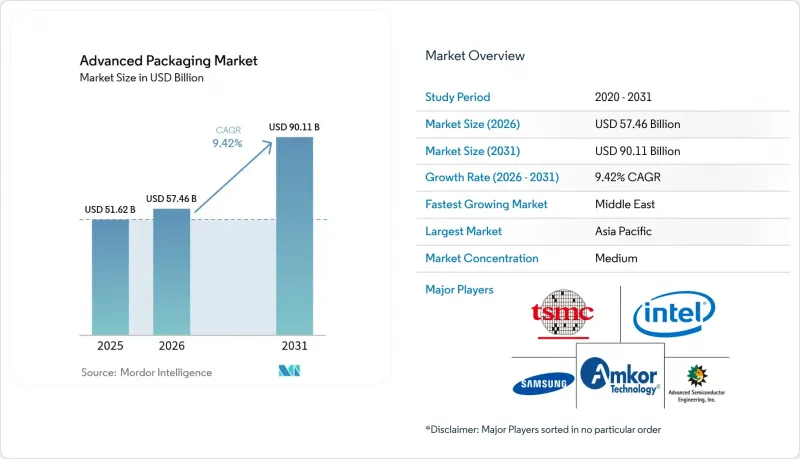
Mordor Intelligence에 의하면, 첨단 패키징 시장 규모는 2025년 516억 2,000만 달러로 평가되었습니다. 2026년에는 574억 6,000만 달러로 확대되어 2026-2031년에 걸쳐 CAGR 9.42%로 성장을 지속하여, 2031년에는 901억 1,000만 달러에 이를 것으로 예측됩니다.
본 보고서는 패키징 플랫폼별(플립칩, 임베디드 다이, 팬-인 WLP, 기타), 최종 사용자 산업별(가전제품, 자동차·EV, 데이터센터·HPC, 기타),디바이스 아키텍처별(2D IC, 2.5D 인터포저, 3D IC), 상호 연결 기술별(솔더 범프, 구리 필러, 하이브리드 본드, 기타), 지역별로 분류되어 있습니다. 시장 예측은 금액(미 달러) 기준으로 제시되어 있습니다.
세계의 첨단 패키징 시장 동향 및 인사이트
AI·HPC 분야의 이종 통합에 대한 수요 증가
치플렛 아키텍처에서는 로직, 메모리, I/O를 고대역폭 인터포저로 연결된 여러 타일로 분할함으로써, 모놀리식 설계로는 전력 제한 범위 내에서 달성할 수 없는 연산 밀도를 실현하고 있습니다. TSMC는 2025년에 NVIDIA의 Hopper 및 Blackwell GPU용으로 1만 5,000장 이상의 CoWoS 웨이퍼를 출하하여 상용화 준비가 완료되었음을 보여주었습니다. 인텔의 Foveros Direct 하이브리드 본딩 기술은 10미크론 이하의 피치를 실현하여 캐시에서 코어까지의 레이턴시를 5ns 이하로 단축했습니다. 서로 다른 노드에서 제조된 로직, 아날로그, RF 타일을 조합함으로써 비용과 시장 출시 시간을 최적화하고 있습니다. 이러한 추세에 힘입어 데이터센터용 가속기 및 소버린 AI 이니셔티브를 뒷받침하는 2.5D 및 3D 플랫폼에서 두 자릿수 성장이 지속되고 있습니다.
소비자용 기기의 소형화에 따른 WLP 보급 촉진
스마트폰 및 웨어러블 기기는 Z축 높이를 6mm 이하로 만드는 것을 목표로 하고 있어, 기판 기반 패키지를 채택할 여지가 없습니다. 팬아웃 웨이퍼 레벨 기술은 I/O를 다이 표면 전체에 재배선함으로써 패키지 두께를 0.4mm 이하로 억제합니다. Apple과 Qualcomm은 이미 대량 생산 프로세서를 팬아웃 방식으로 전환했으며, 툴 비용이 상각됨에 따라 중견 안드로이드 브랜드들도 이를 따르고 있습니다. 웨어러블 생체 센서의 경우, 와이어 본딩을 배제하고 내충격성과 기밀성을 높이는 팬-인-칩 스케일 패키지가 채택되고 있습니다. 각 브랜드가 얇은 두께와 배터리 수명을 우선시하는 가운데, 첨단 패키징 시장에서는 소비자 부문 전체에서 웨이퍼 레벨 패키지의 생산량이 서서히 증가하고 있습니다.
첨단 패키징 라인의 높은 자본 집약도
패널 레벨 공장에서는 리소그래피, 전기도금, 검사 장비에 라인당 5억 달러 이상이 필요하며, 현재의 가동률로는 투자 회수 기간이 5년 이상에 달할 전망입니다. 1,500만 달러를 초과하는 하이브리드 본딩 장비는 시간당 고작 30장의 웨이퍼만 처리할 수 있어 처리량의 병목 현상이 되고 있습니다. 세대 교체가 급속히 진행됨에 따라 감가상각 주기는 3년으로 단축되었으며, 많은 OSAT(수탁 반도체 제조업체)의 영업이익률은 15% 미만에 머물고 있습니다. 임금이 높은 지역에서는 정부 보조금이 프로젝트 비용의 30-40%밖에 충당하지 못하기 때문에 민간 투자자들이 막대한 자금 부족을 메워야만 하는 상황에 처해 있어 그린필드(신규) 확장이 지연되고 있습니다.
부문별 분석
패널 레벨 패키징은 2025년에는 미미한 점유율에 그쳤으나, 첨단 패키징 시장 규모에서 해당 부문은 2026-2031년에 걸쳐 연평균 성장률(CAGR) 9.72%로 확대될 것으로 예측됩니다. 플립칩은 기준 연도에 첨단 패키징 시장 점유율의 41.37%를 차지하며 여전히 수량 면에서 선두를 유지하고 있지만, 그 솔더 범프 피치는 경제적으로 20마이크로미터를 밑돌 수 없기 때문에 AI 가속기 부문에서의 미래성이 제한되고 있습니다. 팬아웃형 웨이퍼 레벨 패키지(WLP)는 스마트폰 및 웨어러블 기기에서 보급이 확대되고 있는 반면, 팬인형 WLP는 비용 효율을 중시하는 RF 모듈을 뒷받침하고 있습니다. PCB 라미네이트에 다이를 매립하는 기술은 20%의 가격 프리미엄을 상쇄할 수 있는 내진동성을 요구하는 자동차용 레이더 설계자들의 주목을 받고 있습니다.
첨단 패키징 시장에서는 실리콘과 동등한 열팽창 계수를 가진 750mm 사방의 유리 기판으로의 스케일업을 통해 다이 핸들링 비용을 40% 절감하는 수단으로서 패널 레벨 형태가 점점 더 주목받고 있습니다. 레이저 비아 가공, 진공 라미네이션, 대면적 스텝 앤 리피트 노광 기술이 아직 목표 수율에 도달하지 못했기 때문에 장비의 성숙도는 여전히 장벽으로 남아 있습니다. 상용화는 2027년 이후로 예상되므로, 공급망 각사는 현재 리드타임이 긴 제조 장비를 잇달아 주문하고 있습니다. 조기 도입 기업들은 데이터센터용 프로세서나 AI 가속기에 주력하고 있는데, 이러한 부문에서는 수율 학습 곡선에 따른 비용 증가가 높은 평균 판매 가격으로 상쇄되기 때문입니다. 패널 플랫폼이 보급되기 전까지는 구리 필러의 개량이 진행되고 있는 그래픽 프로세서 및 ASIC 부문에서 플립 칩이 계속해서 주류를 이룰 것으로 보입니다.
2025년에는 가전제품이 첨단 패키징 시장 규모의 48.77%를 차지했으나, 스마트폰 교체 주기가 장기화됨에 따라 출하 대수 증가세는 정체되는 경향을 보이고 있습니다. 자동차 및 EV 용도는 2031년까지 연평균 성장률(CAGR) 10.11%를 나타낼 것으로 예측되며, 이는 전체 산업 중 가장 높은 성장률입니다. 이는 구리 필러와 하이브리드 본딩을 사용하여 패키징된 실리콘 카바이드 모듈에 의존하는 800V 파워트레인으로의 전환을 반영한 것입니다. 데이터센터 및 HPC 수요는 치플렛 기반 GPU와 코패키지드 옵틱스를 활용하는 AI 추론 워크로드에 힘입어 계속해서 견조한 모습을 보이고 있습니다.
배터리 비용의 하락과 정부의 제로 배출 규제 도입에 따라 차량 1대당 반도체 함유율은 부품표(BOM) 가치의 5%에서 15%로 상승하고 있으며, 그 대부분은 고전압 및 가혹한 열 사이클에 대응하는 첨단 패키지가 차지하고 있습니다. 산업용 IoT 모듈의 경우, 1와트 이하의 소비 전력에 최적화된 시스템 인 패키지(SiP) 형태로 센서, 마이크로컨트롤러, 무선 통신 기능을 통합하고 있습니다. 의료용 웨어러블 기기의 경우, 생체 적합성을 충족하기 위해 기밀형 팬-인 WLP가 채택되고 있습니다. 항공우주 및 방위 부문은 규모는 작지만, 내방사선성 금 와이어 패키지에 대해 프리미엄 가격이 책정되어 있습니다. 자동차 부문의 급속한 성장에 따라 첨단 패키징 산업은 IATF 16949 및 ISO 26262 인증을 받은 파워 모듈 생산 라인으로 설비 투자를 재분배하고 있습니다.
지역별 분석
2025년, 아시아태평양은 첨단 패키징 시장의 60.57%를 차지했습니다. 이는 대만, 중국, 한국, 말레이시아에 집중된 파운드리, 외주 조립·검사 거점, 기판 제조업체의 집적을 반영한 것입니다. 이 지역의 우위는 대만 반도체 제조 회사(TSMC)의 CoWoS와 삼성의 I-Cube 생산 확대에 힘입은 것입니다. 두 회사 모두 AI 가속기 수요를 충족하기 위해 2025년 중 월간 생산 능력을 확대했습니다. 중국의 SMIC(Semiconductor Manufacturing International Corporation)와 장쑤 창장 전자과학기술(Jiangsu Changjiang Electronics Technology)은 국내 스마트폰 및 자동차용 고객을 위해 팬아웃 웨이퍼 레벨 패키징(fan-out wafer-level packaging) 생산 라인을 추가했습니다. 다만, 극자외선(EUV) 리소그래피에 대한 수출 규제로 인해 최첨단 노드에서의 경쟁력은 제약을 받고 있습니다. 아지노모토와 이비덴이 주도하는 일본의 기판 생태계는 플립 칩 및 2.5D 모듈용 첨단 패키징 시장 규모를 뒷받침하는 견고한 소재 공급망을 유지하고 있습니다.
북미에서는 ‘CHIPS and Science Act’에 따라 국내 생산 능력 확충을 위해 390억 달러의 보조금과 750억 달러의 대출 보증이 투입되었으며, 그 대상에 첨단 패키징 시장의 인프라가 명시적으로 포함되어 있어 시장 점유율을 회복하고 있습니다. TSMC의 애리조나 캠퍼스에서는 2025년에 CoWoS 생산이 시작되는 한편, 인텔은 뉴멕시코주와 오리건주에서 Foveros 3D 패키징 생산 라인을 확대되고 있습니다. Amkor의 20억 달러 규모의 애리조나 공장은 자동차용 실리콘 카바이드 파워 모듈과 항공우주 규격 적합 패키지에 주력하고 있습니다. 캐나다와 멕시코는 백엔드 테스트와 복잡도가 낮은 조립 단계에 머물러 있습니다. 따라서 국내 조달 의무와 관련된 첨단 패키징 시장 규모는 북미 대륙 전체에서 꾸준히 확대되고 있습니다.
유럽은 2025년에 소규모 시장 규모에 그쳤으며, 그 중심은 독일 프라운호퍼 연구소의 패널 레벨 파일럿 라인과이탈리아 STMicroelectronics의 조립 사업에 집중되어 있었으나, EU의 ‘칩 법’에 따른 430억 유로 규모의 경기 부양책으로 인해 2030년까지 해당 지역의 반도체 점유율은 두 배로 증가할 전망입니다. 중동 및 아프리카는 기반은 작지만, 아랍에미리트와 사우디아라비아가 정부계 펀드를 활용해 그린필드 팹 및 패키징 공장에 자금을 투입하고 있어, 2031년까지 연평균 성장률(CAGR) 9.61%로 확대될 것으로 예측됩니다. 남미는 테스트 및 기존 조립 단계에 머물러 있으며, 브라질의 Ceitec이 현지 자동차 부품 공급업체에 서비스를 제공합니다. 이러한 전반적인 지리적 분산은 대만에 대한 과도한 의존으로 인한 위험을 완화하고자 하는 고객의 요구를 반영한 것으로, 이에 따라 첨단 패키징 시장은 다지역에 걸친 중복 구성을 향해 나아가고 있으며, 입지 조건이 경쟁상의 차별화 요인으로 작용하고 있습니다.
기타 혜택
- 엑셀 형식 시장 예측(ME) 시트
- 3개월간의 애널리스트 지원
자주 묻는 질문
목차
제1장 서론
제2장 조사 방법
제3장 주요 요약
제4장 시장 구도
제5장 시장 규모 및 성장 예측
제6장 경쟁 구도
제7장 시장 기회 및 향후 전망
KTH 26.09.04According to Mordor Intelligence, the advanced packaging market size is expected to grow from USD 51.62 billion in 2025 to USD 57.46 billion in 2026 and is forecast to reach USD 90.11 billion by 2031 at 9.42% CAGR over 2026-2031.
This report is Segmented by Packaging Platform (Flip-Chip, Embedded Die, Fan-In WLP, and More), End-User Industry (Consumer Electronics, Automotive and EV, Data Center and HPC, and More), Device Architecture (2D IC, 2. 5D Interposer, and 3D IC), Interconnect Technology (Solder Bump, Copper Pillar, Hybrid Bond, and More), and Geography. The Market Forecasts are Provided in Terms of Value (USD).
Global Advanced Packaging Market Trends and Insights
Rising Demand for Heterogeneous Integration for AI and HPC
Chiplet architectures now partition logic, memory and I/O across multiple tiles connected by high-bandwidth interposers, enabling compute density that monolithic designs cannot reach within power limits. TSMC shipped more than 15 000 CoWoS wafers in 2025 for NVIDIA's Hopper and Blackwell GPUs, highlighting commercial readiness. Intel's Foveros Direct hybrid-bond technology achieves sub-10-micron pitch, cutting cache-to-core latency below 5 ns. Mix-and-match logic, analog and RF tiles fabricated on different nodes optimize cost and time-to-market. The trend sustains double-digit expansion in 2.5D and 3D platforms that underpin data-center accelerators and sovereign-AI initiatives.
Miniaturization of Consumer Devices Boosting WLP Adoption
Smartphones and wearables target sub-6 mm Z-heights, leaving no room for substrate-based packages. Fan-out wafer-level technology redistributes I/O across the die surface, achieving package thickness below 0.4 mm. Apple and Qualcomm have already migrated high-volume processors to fan-out, and mid-tier Android brands follow as tooling costs amortize. Wearable biosensors are adopting fan-in chip-scale packages that eliminate wire bonds, enhancing shock resistance and hermeticity. As brands prioritize thinness and battery life, the advanced packaging market gains incremental wafer-level volume across consumer segments.
High Capital Intensity of Advanced Packaging Lines
Panel-level factories demand more than USD 500 million per line for lithography, electroplating and test equipment, stretching payback beyond five years at today's utilizations. Hybrid-bonding tools priced above USD 15 million process only 30 wafers per hour, creating throughput pinch points. Depreciation cycles compress to three years because generations turn quickly, pushing operating margins for many OSATs below 15%. Government subsidies cover only 30-40% of project cost in high-wage regions, forcing private investors to bridge large funding gaps and delaying greenfield expansion.
Other drivers and restraints analyzed in the detailed report include:
- Government Semiconductor Subsidies (CHIPS and EU Chips Acts)
- EV Power-Electronics Reliability Needs
- Industry Consolidation Squeezing Outsourced Margins
For complete list of drivers and restraints, kindly check the Table Of Contents.
Segment Analysis
Panel-level packaging accounted for a modest share in 2025, yet its segment within the advanced packaging market size is projected to expand at a 9.72% CAGR between 2026 and 2031. Flip-chip remained the volume leader with 41.37% of advanced packaging market share in the base year, but its solder-bump pitch cannot drop below 20 µm economically, limiting its future in AI accelerators. Fan-out wafer-level packages thrive in smartphones and wearables, while fan-in WLP supports cost-sensitive RF modules. Embedded-die in PCB laminates attracts automotive radar designers seeking vibration tolerance that offsets a 20% price premium.
The advanced packaging market increasingly views panel-level formats as a route to 40% lower die-handling cost by scaling to 750-mm-square glass substrates whose thermal expansion matches silicon. Equipment maturity remains a gating factor because laser-via drilling, vacuum lamination and large-field step-and-repeat lithography have yet to hit target yields. Commercial readiness is expected after 2027, so supply chains are lining up long-lead tooling orders today. Early adopters focus on data-center processors and AI accelerators where the cost penalty of yield learning curves is amortized over high average selling prices. Until panel platforms scale, flip-chip will keep dominating graphics processors and ASICs albeit with incremental copper-pillar refinements.
Consumer electronics captured 48.77% of the advanced packaging market size in 2025, yet its unit growth is flattening as smartphone refresh cycles lengthen. Automotive and EV applications are forecast to register a 10.11% CAGR through 2031, the fastest across all industries, reflecting the shift to 800-volt powertrains that rely on silicon-carbide modules packaged with copper pillars and hybrid bonds. Data-center and HPC demand remains robust, fueled by AI inference workloads that exploit chiplet-based GPUs and co-packaged optics.
As battery costs fall and governments impose zero-emission mandates, semiconductor content per vehicle is rising from 5% to 15% of bill-of-materials value, most of which involves advanced packages handling high voltages and harsh thermal cycles. Industrial IoT modules integrate sensors, microcontrollers and radios in system-in-package formats optimized for sub-1 W power envelopes. Healthcare wearables add hermetic fan-in WLP to satisfy biocompatibility. Aerospace and defense, while small, command premium pricing for radiation-hardened, gold-wire packages. The automotive surge ensures that the advanced packaging industry reallocates capex toward power module lines certified under IATF 16949 and ISO 26262.
Complete Report Scope:
- By Packaging Platform
- Flip-Chip
- Embedded Die
- Fan-in WLP
- Fan-out WLP
- 2.5D / 3D
- System-in-Package (SiP)
- Panel Level Packaging (PLP)
- By End-User Industry
- Consumer Electronics
- Automotive and EV
- Data Center and HPC
- Industrial and IoT
- Healthcare / Med-tech
- Aerospace and Defense
- By Device Architecture
- 2D IC
- 2.5D Interposer
- 3D IC (TSV / Hybrid-Bond)
- By Interconnect Technology
- Solder Bump
- Copper Pillar
- Hybrid Bond
- Micro-bump-less Direct Bond
- By Geography
- North America
- United States
- Canada
- Mexico
- South America
- Brazil
- Argentina
- Rest of South America
- Europe
- Germany
- United Kingdom
- France
- Italy
- Spain
- Rest of Europe
- Asia-Pacific
- China
- India
- Japan
- South Korea
- Australia
- Rest of Asia-Pacific
- Middle East
- United Arab Emirates
- Saudi Arabia
- Rest of Middle East
- Middle East
- South Africa
- Egypt
- Rest of Africa
- North America
Geography Analysis
Asia-Pacific contributed 60.57% of the advanced packaging market in 2025, reflecting deep clusters of foundries, outsourced assembly and test sites, and substrate makers located in Taiwan, China, South Korea and Malaysia. The region's dominance is anchored by Taiwan Semiconductor Manufacturing Company's CoWoS and Samsung's I-Cube ramps, both of which expanded monthly capacity during 2025 to satisfy AI-accelerator demand. China's Semiconductor Manufacturing International Corporation and Jiangsu Changjiang Electronics Technology added fan-out wafer-level lines for domestic smartphone and automotive customers, even though export-control limits on extreme-ultraviolet lithography curb their competitiveness at the leading nodes. Japan's substrate ecosystem, led by Ajinomoto and Ibiden, sustains a resilient material supply chain that underpins the advanced packaging market size for flip-chip and 2.5D modules.
North America is regaining share as the CHIPS and Science Act channels USD 39 billion in grants and USD 75 billion in loan guarantees toward on-shore capacity, explicitly including advanced packaging market infrastructure. TSMC's Arizona campus begins CoWoS production in 2025, while Intel expands Foveros 3D-packaging lines in New Mexico and Oregon. Amkor's USD 2 billion Arizona plant focuses on automotive silicon-carbide power modules and aerospace-qualified packages. Canada and Mexico remain limited to back-end test and low-complexity assembly. The advanced packaging market size tied to domestic-content mandates is therefore growing steadily across the continent.
Europe captured modest value in 2025, concentrated in Germany's Fraunhofer panel-level pilot line and STMicroelectronics assembly in Italy, yet the EU Chips Act's EUR 43 billion stimulus is set to double regional semiconductor share by 2030. The Middle East and Africa held a small base but is forecast to rise at 9.61% CAGR to 2031 as the United Arab Emirates and Saudi Arabia use sovereign-wealth funds to fund green-field fabs and packaging plants. South America stays limited to test and legacy assembly, with Brazil's Ceitec serving local automotive suppliers. Overall geographic dispersion reflects customer imperatives to derisk over-reliance on Taiwan, driving the advanced packaging market toward multi-regional redundancy and making site location a competitive differentiator.
- Amkor Technology Inc.
- Taiwan Semiconductor Manufacturing Company Limited
- Advanced Semiconductor Engineering Inc.
- JCET Group Co. Ltd.
- Samsung Electronics Co. Ltd.
- Intel Corporation
- Chipbond Technology Corporation
- ChipMOS Technologies Inc.
- Powertech Technology Inc.
- TongFu Microelectronics Co. Ltd.
- Nepes Corporation
- STATS ChipPAC Pte. Ltd.
- Siliconware Precision Industries Co. Ltd.
- UTAC Holdings Ltd.
- Walton Advanced Engineering Inc.
- Xintec Inc.
- Tianshui Huatian Technology Co. Ltd.
- King Yuan Electronics Co. Ltd.
- GlobalFoundries Inc.
- Semiconductor Manufacturing International Corporation
- SFA Semicon Co. Ltd.
- Nantong Fujitsu Microelectronics Co. Ltd.
- Hana Micron Inc.
- Unisem (M) Berhad
- Deca Technologies Inc.
- Veeco Instruments Inc.
Additional Benefits:
- The market estimate (ME) sheet in Excel format
- 3 months of analyst support
TABLE OF CONTENTS
1 INTRODUCTION
- 1.1 Study Assumptions and Market Definition
- 1.2 Scope of the Study
2 RESEARCH METHODOLOGY
3 EXECUTIVE SUMMARY
4 MARKET LANDSCAPE
- 4.1 Market Overview
- 4.2 Market Drivers
- 4.2.1 Rising Demand For Heterogeneous Integration For AI and HPC
- 4.2.2 Miniaturization of Consumer Devices Boosting WLP Adoption
- 4.2.3 Government Semiconductor Subsidies (E.G., CHIPS And EU Chips Acts)
- 4.2.4 EV Power-Electronics Reliability Needs
- 4.2.5 Emerging Glass-Core Substrates Enabling Panel-Level Packaging
- 4.2.6 Co-Packaged Optics Demand In Hyperscale Data Centers
- 4.3 Market Restraints
- 4.3.1 High Capital Intensity of Advanced Packaging Lines
- 4.3.2 Industry Consolidation Squeezing Outsourced Margins
- 4.3.3 BT-Resin Substrate Capacity Bottlenecks
- 4.3.4 Shortage of Advanced Assembly Talent
- 4.4 Value Chain Analysis
- 4.5 Regulatory Landscape
- 4.6 Technological Outlook
- 4.7 Porter's Five Forces
- 4.7.1 Bargaining Power of Suppliers
- 4.7.2 Bargaining Power of Buyers
- 4.7.3 Threat of New Entrants
- 4.7.4 Threat of Substitutes
- 4.7.5 Intensity of Competitive Rivalry
5 MARKET SIZE AND GROWTH FORECASTS (VALUE)
- 5.1 By Packaging Platform
- 5.1.1 Flip-Chip
- 5.1.2 Embedded Die
- 5.1.3 Fan-in WLP
- 5.1.4 Fan-out WLP
- 5.1.5 2.5D / 3D
- 5.1.6 System-in-Package (SiP)
- 5.1.7 Panel Level Packaging (PLP)
- 5.2 By End-User Industry
- 5.2.1 Consumer Electronics
- 5.2.2 Automotive and EV
- 5.2.3 Data Center and HPC
- 5.2.4 Industrial and IoT
- 5.2.5 Healthcare / Med-tech
- 5.2.6 Aerospace and Defense
- 5.3 By Device Architecture
- 5.3.1 2D IC
- 5.3.2 2.5D Interposer
- 5.3.3 3D IC (TSV / Hybrid-Bond)
- 5.4 By Interconnect Technology
- 5.4.1 Solder Bump
- 5.4.2 Copper Pillar
- 5.4.3 Hybrid Bond
- 5.4.4 Micro-bump-less Direct Bond
- 5.5 By Geography
- 5.5.1 North America
- 5.5.1.1 United States
- 5.5.1.2 Canada
- 5.5.1.3 Mexico
- 5.5.2 South America
- 5.5.2.1 Brazil
- 5.5.2.2 Argentina
- 5.5.2.3 Rest of South America
- 5.5.3 Europe
- 5.5.3.1 Germany
- 5.5.3.2 United Kingdom
- 5.5.3.3 France
- 5.5.3.4 Italy
- 5.5.3.5 Spain
- 5.5.3.6 Rest of Europe
- 5.5.4 Asia-Pacific
- 5.5.4.1 China
- 5.5.4.2 India
- 5.5.4.3 Japan
- 5.5.4.4 South Korea
- 5.5.4.5 Australia
- 5.5.4.6 Rest of Asia-Pacific
- 5.5.5 Middle East
- 5.5.5.1 United Arab Emirates
- 5.5.5.2 Saudi Arabia
- 5.5.5.3 Rest of Middle East
- 5.5.6 Middle East
- 5.5.6.1 South Africa
- 5.5.6.2 Egypt
- 5.5.6.3 Rest of Africa
- 5.5.1 North America
6 COMPETITIVE LANDSCAPE
- 6.1 Market Concentration
- 6.2 Strategic Moves
- 6.3 Market Share Analysis
- 6.4 Company Profiles (includes Global level Overview, Market level overview, Core Segments, Financials as available, Strategic Information, Market Rank/Share for key companies, Products and Services, and Recent Developments)
- 6.4.1 Amkor Technology Inc.
- 6.4.2 Taiwan Semiconductor Manufacturing Company Limited
- 6.4.3 Advanced Semiconductor Engineering Inc.
- 6.4.4 JCET Group Co. Ltd.
- 6.4.5 Samsung Electronics Co. Ltd.
- 6.4.6 Intel Corporation
- 6.4.7 Chipbond Technology Corporation
- 6.4.8 ChipMOS Technologies Inc.
- 6.4.9 Powertech Technology Inc.
- 6.4.10 TongFu Microelectronics Co. Ltd.
- 6.4.11 Nepes Corporation
- 6.4.12 STATS ChipPAC Pte. Ltd.
- 6.4.13 Siliconware Precision Industries Co. Ltd.
- 6.4.14 UTAC Holdings Ltd.
- 6.4.15 Walton Advanced Engineering Inc.
- 6.4.16 Xintec Inc.
- 6.4.17 Tianshui Huatian Technology Co. Ltd.
- 6.4.18 King Yuan Electronics Co. Ltd.
- 6.4.19 GlobalFoundries Inc.
- 6.4.20 Semiconductor Manufacturing International Corporation
- 6.4.21 SFA Semicon Co. Ltd.
- 6.4.22 Nantong Fujitsu Microelectronics Co. Ltd.
- 6.4.23 Hana Micron Inc.
- 6.4.24 Unisem (M) Berhad
- 6.4.25 Deca Technologies Inc.
- 6.4.26 Veeco Instruments Inc.
7 Market Opportunities and Future Outlook
- 7.1 White-space and Unmet-Need Assessment