

|
시장보고서
상품코드
2119578
아메리카의 반도체 디바이스 : 시장 점유율 분석, 업계 동향과 통계, 성장 예측(2026-2031년)Americas Semiconductor Device - Market Share Analysis, Industry Trends & Statistics, Growth Forecasts (2026 - 2031) |
||||||
 Mordor Intelligence
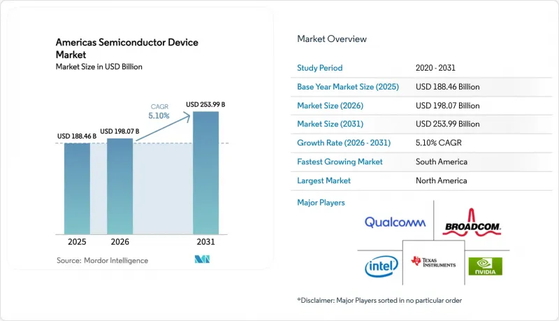
Mordor Intelligence에 따르면 아메리카의 반도체 디바이스 시장 규모는 2025년 1,884억 6,000만 달러에서 2026년에는 1,980억 7,000만 달러로 확대하며, 2026-2031년에 CAGR 5.1%로 추이하며, 2031년에는 2,539억 9,000만 달러에 달할 것으로 예측됩니다.
이 보고서는 디바이스 유형별(디스크리트 반도체, 옵토일렉트로닉스, 센서, 집적회로), 웨이퍼 크기별(200mm 이하, 300mm, 450mm 이상), 공정 노드별(65nm 이상, 45-28nm, 22-16nm, 기타),반도체 소재(실리콘, 실리콘 카바이드, 기타), 최종사용자 산업(자동차, 통신, 소비자용, 산업용, 기타) 및 지역(북미, 남미)별로 분류되어 있습니다.
아메리카 반도체 디바이스 시장의 동향과 인사이트
CHIPS법에 힘입은 북미 지역의 제조 능력 확대
‘CHIPS and Science Act’에 기반한 대규모 연방 정부의 인센티브 정책으로, 2032년까지 국내 웨이퍼 생산량을 3배로 늘리는 것을 목표로 4,500억 달러가 넘는 민간 투자가 유치되었습니다. 인텔은 여러 주에 걸친 확장 계획에 대해 85억 달러의 보조금을 확보했으며, TSMC는 애리조나주의 2개 메가팹에 대해 66억 달러의 보조금을 받았습니다. 리드 타임을 단축하기 위해 40개 이상의 1차 화학·장비 제조업체가 인근에 거점을 마련했으며, 이러한 프로젝트를 중심으로 공급업체 생태계가 형성되었습니다. 이러한 클러스터화를 통해 물류 비용 개선과 기술 이전 가속화가 도모되었으나, 특수 가스 및 화학 약품의 60%를 수입에 의존하는 상황은 변하지 않았으며, 국내 소재 생산 능력 확충을 위한 새로운 설비 투자가 여전히 필요했습니다. 결국, 이러한 투자의 급증으로 북미 및 남미의 반도체 디바이스 시장은 자원 제약으로부터 완전히 격리되지는 못했으나, 더 높은 수준의 자급자족 체제를 구축할 수 있는 기반이 마련되었습니다.
멕시코 및 브라질의 ADAS 탑재 차량 수요
전동화와 레벨 2 운전 지원 시스템의 도입으로, 2024년에는 멕시코 및 브라질의 주요 조립 라인에서 차량 1대당 자동차용 반도체 탑재량이 35% 증가했습니다. 현지 공장에는 높은 신뢰성의 마이크로컨트롤러와 파워 디바이스가 필요한 레이더, 라이더, 이미지 센서 어레이가 탑재되었습니다. 보쉬와 콘티넨탈은 최대 25%까지 인상될 가능성이 있는 수입 관세를 완화하기 위해 현지 패키징 라인에 대한 합작 투자를 추진했습니다. 정책 입안자들은 자동차용 칩에 대한 추가 세액 공제를 시사하며, 생산 능력의 추가 확대를 촉진했습니다. 그 결과, 자동차 관련 수주가 북미 및 남미의 반도체 소자 시장을 가전제품의 경기 변동으로부터 보호했으며, 중기적으로 확실한 수익 상승을 가져왔습니다.
미국 남서부 팹의 물·전력 공급 제약
애리조나주와 텍사스주의 신설 팹에서는 하루 최대 1,000만 갤런의 초순수가 소비되어 일반 시민들과의 직접적인 경쟁이 발생했습니다. 인텔은 공정 용수의 90%를 재활용하는 시스템에 2억 달러를 투자했으나, 이러한 환경 프로젝트는 영업 비용을 2% 상승시켰고, 장기적인 가뭄의 위험을 완전히 완화할 수는 없었습니다. 전력 수요 증가로 인해 전력 회사는 송전망 업그레이드를 가속화할 수밖에 없었고, 이는 생산 비용을 더욱 상승시켰습니다. 이러한 제약으로 인해 ‘CHIPS법’의 인센티브에 따른 실질적인 생산 능력 증가는 축소되었으며, 장기적으로는 북미 및 남미 반도체 소자 시장의 비용 경쟁력이 위협받게 되었습니다.
부문별 분석
집적회로(IC)는 2025년에 매출의 80.65%를 차지하고 연평균 성장률(CAGR) 7.45%로 확대될 것으로 예측되며, 북미 및 남미의 반도체 디바이스 시장 규모는 여전히 복잡한 로직 및 메모리 분야에 크게 치우쳐 있습니다. AI 훈련, 자율주행, 산업용 엣지 컴퓨팅 각 분야에서 시스템당 실리콘 사용량이 증가하여 고대역폭 메모리 및 추론 가속기의 평균 판매 가격을 끌어올렸습니다. 디스크리트 파워 디바이스는 시장 규모는 작지만, 전기자동차 분야에서 실리콘 카바이드(SiC) 및 질화 갈륨(GaN) 스위치가 실리콘 IGBT를 대체하여 파워트레인의 효율과 열 여유를 향상시킴으로써 전략적 중요성이 높아졌습니다. 또한 북미 및 남미의 반도체 소자 업계에서는 옵토일렉트로닉스가 LiDAR 및 이미지 센싱 분야로 확대되면서, 주기적인 변동이 나타나는 스마트폰 분야에 대한 다각화를 더욱 촉진했습니다.
임베디드 애플리케이션의 다양화가 진행됨에 따라 센서 출하량은 견고한 추세를 보였으나, 많은 설계가 자산의 감가상각이 완료된 성숙한 공정 라인에 의존하고 있었기 때문에 가격 압박은 지속되었습니다. 아날로그 IC는 수십년에 걸친 공급 연속성이 요구되는 기존의 자동차용 및 산업용 소켓을 통해 안정적인 현금 흐름을 창출했습니다. 한편, 로직 및 메모리는 하이퍼스케일 기업의 설비 투자 주기와 연동되어 더 큰 변동을 보였습니다. 이러한 변동에도 불구하고 집적회로(IC) 분야에서는 생태계에 대한 꾸준한 투자가 이루어졌으며, 아메리카 반도체 디바이스 시장에서 설계 인력의 정착이 강화되었습니다.
2025년에는 300mm 라인이 생산의 57.60%를 차지하며, 거의 모든 최첨단 노드를 지원하고 아메리카 반도체 디바이스 시장 규모에서 가장 큰 비중을 차지했습니다. 각 파운드리 업체들은 성숙한 아날로그 제품을 200mm 기판에서 300mm 기판으로 전환한 결과, 단위 비용이 30% 감소하여 매출 총이익률의 여유가 확대되었습니다. 한편, 장비 제조사들은 450mm 파일럿 툴의 개량을 추진했습니다. 이 직경은 여전히 틈새 분야에 머물러 있지만, 제조사들이 더 큰 규모의 경제를 추구하는 가운데 2031년까지 연평균 성장률(CAGR)은 16.4%로 전망됩니다.
<=200mm 팹은 자동차 및 산업 분야 구매자들이 순수한 연산 밀도보다 검증된 신뢰성을 중시했으므로 여전히 중요한 위치를 차지하고 있었습니다. 또한 이러한 팹은 멕시코에서의 백엔드 조립 니어쇼어링의 혜택도 누리고 있으며, 이를 통해 레거시 부품의 사이클 타임이 단축되었습니다. 북미 및 남미의 반도체 디바이스 시장은 특정 노드나 웨이퍼 크기에서 발생할 수 있는 주기적인 공급 과잉에 대비하기 위해, 각 직경에 걸친 투자의 균형을 지속적으로 유지해 왔습니다.
기타 혜택:
- 엑셀 형식의 시장 예측(ME) 시트
- 3개월간의 애널리스트 지원
자주 묻는 질문
목차
제1장 서론
제2장 조사 방법
제3장 개요
제4장 시장 구도
제5장 시장 규모와 성장 예측
제6장 경쟁 구도
제7장 시장 기회와 향후 전망
KSA 26.09.02According to Mordor Intelligence, the americas semiconductor device market size is expected to grow from USD 188.46 billion in 2025 to USD 198.07 billion in 2026 and is forecast to reach USD 253.99 billion by 2031 at 5.1% CAGR over 2026-2031.
This report is Segmented by Device Type (Discrete Semiconductors, Optoelectronics, Sensors, and Integrated Circuits), Wafer Size (<= 200 Mm, 300 Mm, and >= 450 Mm), Technology Node (>= 65 Nm, 45-28 Nm, 22-16 Nm, and More), Semiconductor Material (Silicon, Silicon Carbide, and More), End-User Vertical (Automotive, Communication, Consumer, Industrial, and More), and by Region (North America, and South America).
Americas Semiconductor Device Market Trends and Insights
CHIPS Act-Driven Fabrication Capacity Expansion in North America
Massive federal incentives under the CHIPS and Science Act unlocked more than USD 450 billion in private commitments that aimed to triple domestic wafer output by 2032. Intel secured USD 8.5 billion in grants for multistate expansions, while TSMC received USD 6.6 billion for its two Arizona megafabs. Supplier ecosystems clustered around those projects, as over 40 tier-one chemical and equipment firms co-located nearby to shorten lead times. These clusters improved logistics costs and accelerated knowledge transfer, yet a 60% dependence on imported specialty gases and chemicals still forced new capital outlays for on-shore materials capacity. Ultimately, the investment surge positioned the Americas semiconductor device market for higher self-sufficiency without fully insulating it from resource constraints.
ADAS-Enabled Vehicle Demand in Mexico and Brazil
Electrification and Level-2 driver-assistance adoption pushed automotive semiconductor content per vehicle up 35% in leading Mexican and Brazilian assembly lines during 2024. Local plants integrated radar, lidar, and image-sensor arrays that required high-reliability microcontrollers and power devices. Bosch and Continental pursued joint ventures for on-shore packaging lines to mitigate import tariffs that could rise to 25%. Policymakers signalled additional fiscal credits for auto-grade chips, encouraging further capacity moves. As a result, automotive orders buffered the Americas semiconductor device market against consumer-electronics cyclicality and created a dependable mid-term revenue uplift.
Water and Power Supply Constraints in U.S. Southwest Fabs
New fabs in Arizona and Texas consumed up to 10 million gallons of ultrapure water daily, creating direct competition with municipal users. Intel invested USD 200 million in reclamation systems that recycled 90% of process water, yet those eco-projects added 2% to operating expenses and did not fully mitigate long-term drought risk. Rising electricity demand forced utilities to accelerate grid upgrades, further lifting production costs. These constraints reduced effective capacity gains from CHIPS Act incentives and threatened the cost competitiveness of the Americas semiconductor device market over the long horizon.
Other drivers and restraints analyzed in the detailed report include:
- 5G Stand-Alone Roll-out Elevating RF Front-End IC Consumption
- Hyperscale AI Server Build-out Increasing HBM and GPU Requirements
- Scarcity of Skilled Semiconductor Engineers across the Americas
For complete list of drivers and restraints, kindly check the Table Of Contents.
Segment Analysis
Integrated circuits captured 80.65% revenue in 2025 and advanced on a 7.45% CAGR projection, keeping the Americas semiconductor device market size firmly weighted toward complex logic and memory. AI training, autonomous driving, and industrial edge computing each increased silicon content per system, lifting average selling prices for high-bandwidth memory and inference accelerators. Discrete power devices, though smaller in value, gained strategic importance as silicon-carbide and gallium-nitride switches replaced silicon IGBTs in electric vehicles, improving powertrain efficiency and thermal margins. The Americas semiconductor device industry also saw optoelectronics broaden into lidar and image-sensing, providing incremental diversification against the cyclic smartphone segment.
A widening array of embedded applications drove resilient sensor volumes, yet price pressure persisted because many designs relied on mature process lines with fully depreciated assets. Analog ICs offered stable cash flow due to legacy automotive and industrial sockets that require decades-long supply continuity. Meanwhile, logic and memory displayed higher volatility in line with hyperscale capex cycles. Despite those swings, the integrated-circuits category delivered steady ecosystem investment, reinforcing design talent retention inside the Americas semiconductor device market.
In 2025, 300 mm lines accounted for 57.60% of production and underpinned nearly every leading-edge node, anchoring the largest slice of the Americas semiconductor device market size. Foundries noted 30% lower unit costs after migrating mature analog products from 200 mm to 300 mm substrates, widening gross-margin cushions. Equipment makers concurrently refined 450 mm pilot tools; although that diameter remained niche, it logged a 16.4% CAGR outlook to 2031 as manufacturers chased further economies of scale.
<=200 mm fabs preserved relevance because automotive and industrial buyers valued proven reliability over raw compute density. These fabs also benefited from the near-shoring of backend assembly in Mexico, which reduced cycle times for legacy components. The Americas semiconductor device market continued to balance investments across diameters to hedge against cyclical oversupply at any single node or wafer size.
Complete Report Scope:
- By Device Type
- Discrete Semiconductors
- Optoelectronics
- Sensors
- Integrated Circuits
- Analog ICs
- Logic ICs
- Memory ICs
- Micro ICs
- Microprocessors (MPU)
- Microcontrollers (MCU)
- Digital Signal Processors (DSP)
- By Wafer Size
- <= 200 mm
- 300 mm
- >= 450 mm
- By Technology Node
- >= 65 nm
- 45-28 nm
- 22-16 nm
- 10-7 nm
- <= 5 nm
- By Semiconductor Material
- Silicon (Si)
- Silicon Carbide (SiC)
- Gallium Nitride (GaN)
- Others (GaAs, InP, etc.)
- By End-User Vertical
- Automotive
- Communication (Wired and Wireless)
- Consumer Electronics
- Industrial
- Computing and Data Storage
- Aerospace and Defense
- Healthcare and Medical Devices
- By Region
- North America
- United States
- Canada
- South America
- Brazil
- Argentina
- Mexico
- Rest of South America
- North America
List of Companies Covered in this Report:
- Intel Corporation
- NVIDIA Corporation
- Qualcomm Incorporated
- Micron Technology Inc.
- Texas Instruments Incorporated
- Broadcom Inc.
- Advanced Micro Devices Inc.
- onsemi (ON Semiconductor Corporation)
- NXP Semiconductors N.V.
- Infineon Technologies AG
- STMicroelectronics N.V.
- Analog Devices Inc.
- Microchip Technology Inc.
- Skyworks Solutions Inc.
- GlobalFoundries Inc.
- Taiwan Semiconductor Manufacturing Company Limited
- Samsung Electronics Co., Ltd.
- Marvell Technology Inc.
- Monolithic Power Systems
- Wolfspeed Inc.
- Lattice Semiconductor
Additional Benefits:
- The market estimate (ME) sheet in Excel format
- 3 months of analyst support
TABLE OF CONTENTS
1 INTRODUCTION
- 1.1 Study Assumptions and Market Definition
- 1.2 Scope of the Study
2 RESEARCH METHODOLOGY
3 EXECUTIVE SUMMARY
4 MARKET LANDSCAPE
- 4.1 Market Overview
- 4.2 Market Drivers
- 4.2.1 CHIPS Act-Driven Fabrication Capacity Expansion in North America
- 4.2.2 ADAS-Enabled Vehicle Demand in Mexico and Brazil
- 4.2.3 5G Stand-Alone Roll-out Elevating RF Front-End IC Consumption
- 4.2.4 Hyperscale AI Server Build-out Increasing HBM and GPU Requirements
- 4.2.5 Renewable-Energy Incentives Boosting Power Semiconductor Adoption in Brazil and Chile
- 4.2.6 Nearshoring of Backend Assembly and Test to Mexico
- 4.3 Market Restraints
- 4.3.1 Water and Power Supply Constraints in US Southwest Fabs
- 4.3.2 Scarcity of Skilled Semiconductor Engineers across Americas
- 4.3.3 Export Controls on Advanced Equipment and IP
- 4.3.4 Volatile Silicon Wafer Pricing due to Limited Regional Supply
- 4.4 Value Chain Analysis
- 4.5 Regulatory Outlook
- 4.6 Porter's Five Forces
- 4.6.1 Bargaining Power of Suppliers
- 4.6.2 Bargaining Power of Buyers
- 4.6.3 Threat of New Entrants
- 4.6.4 Threat of Substitutes
- 4.6.5 Intensity of Competitive Rivalry
- 4.7 Investment and Capacity Analysis
- 4.8 Impact of Macroeconomic Factors
5 MARKET SIZE AND GROWTH FORECASTS (VALUE)
- 5.1 By Device Type
- 5.1.1 Discrete Semiconductors
- 5.1.2 Optoelectronics
- 5.1.3 Sensors
- 5.1.4 Integrated Circuits
- 5.1.4.1 Analog ICs
- 5.1.4.2 Logic ICs
- 5.1.4.3 Memory ICs
- 5.1.4.4 Micro ICs
- 5.1.4.4.1 Microprocessors (MPU)
- 5.1.4.4.2 Microcontrollers (MCU)
- 5.1.4.4.3 Digital Signal Processors (DSP)
- 5.2 By Wafer Size
- 5.2.1 <= 200 mm
- 5.2.2 300 mm
- 5.2.3 >= 450 mm
- 5.3 By Technology Node
- 5.3.1 >= 65 nm
- 5.3.2 45-28 nm
- 5.3.3 22-16 nm
- 5.3.4 10-7 nm
- 5.3.5 <= 5 nm
- 5.4 By Semiconductor Material
- 5.4.1 Silicon (Si)
- 5.4.2 Silicon Carbide (SiC)
- 5.4.3 Gallium Nitride (GaN)
- 5.4.4 Others (GaAs, InP, etc.)
- 5.5 By End-User Vertical
- 5.5.1 Automotive
- 5.5.2 Communication (Wired and Wireless)
- 5.5.3 Consumer Electronics
- 5.5.4 Industrial
- 5.5.5 Computing and Data Storage
- 5.5.6 Aerospace and Defense
- 5.5.7 Healthcare and Medical Devices
- 5.6 By Region
- 5.6.1 North America
- 5.6.1.1 United States
- 5.6.1.2 Canada
- 5.6.2 South America
- 5.6.2.1 Brazil
- 5.6.2.2 Argentina
- 5.6.2.3 Mexico
- 5.6.2.4 Rest of South America
- 5.6.1 North America
6 COMPETITIVE LANDSCAPE
- 6.1 Market Concentration
- 6.2 Strategic Moves
- 6.3 Market Share Analysis
- 6.4 Company Profiles (includes Global level Overview, Market level overview, Core Segments, Financials as available, Strategic Information, Market Rank/Share for key companies, Products and Services, and Recent Developments)
- 6.4.1 Intel Corporation
- 6.4.2 NVIDIA Corporation
- 6.4.3 Qualcomm Incorporated
- 6.4.4 Micron Technology Inc.
- 6.4.5 Texas Instruments Incorporated
- 6.4.6 Broadcom Inc.
- 6.4.7 Advanced Micro Devices Inc.
- 6.4.8 onsemi (ON Semiconductor Corporation)
- 6.4.9 NXP Semiconductors N.V.
- 6.4.10 Infineon Technologies AG
- 6.4.11 STMicroelectronics N.V.
- 6.4.12 Analog Devices Inc.
- 6.4.13 Microchip Technology Inc.
- 6.4.14 Skyworks Solutions Inc.
- 6.4.15 GlobalFoundries Inc.
- 6.4.16 Taiwan Semiconductor Manufacturing Company Limited
- 6.4.17 Samsung Electronics Co., Ltd.
- 6.4.18 Marvell Technology Inc.
- 6.4.19 Monolithic Power Systems
- 6.4.20 Wolfspeed Inc.
- 6.4.21 Lattice Semiconductor
7 MARKET OPPORTUNITIES AND FUTURE OUTLOOK
- 7.1 White-space and Unmet-Need Assessment


