
|
시장보고서
상품코드
2124320
감광성 반도체 디바이스 시장 : 시장 점유율 분석, 업계 동향 및 통계, 성장 예측(2026-2031년)Photosensitive Semiconductor Device - Market Share Analysis, Industry Trends & Statistics, Growth Forecasts (2026 - 2031) |
||||||
 Mordor Intelligence
Mordor Intelligence에 의하면, 감광성 반도체 디바이스 시장 규모는 2026년에 42억 1,000만 달러로 추정되고, 2031년까지 52억 2,000만 달러로 성장할 것으로 예측되며, 예측 기간 중 연평균 복합 성장률(CAGR)은 4.35%를 기록할 전망입니다.
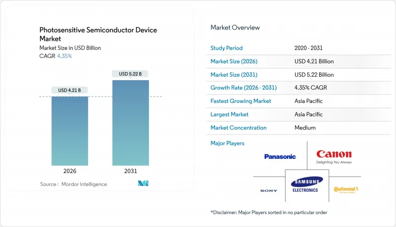
본 보고서는 소자별(포토셀, 포토다이오드, 포토트랜지스터 등), 소재별(실리콘, 게르마늄 등), 작동 모드별(광전력, 광전도, 애벌랜치), 용도별(광통신, 자동차 등), 최종 사용자별(자동차 OEM, 소비자용 전자기기 등), 지역별로 분류되어 있습니다. 시장 예측은 금액(달러) 기준으로 제시되어 있습니다.
세계의 감광성 반도체 디바이스 시장 동향 및 인사이트
자동차용 ADAS 및 LiDAR 채택 확대
2025년 1-3분기 동안, 4만 달러 미만 가격대의 중국산 스포츠 유틸리티 차량(SUV)에 솔리드 스테이트 스캐너가 채택됨에 따라 LiDAR 출하 대수는 83만 대에 달했습니다. 2027년형 모델까지 자동 긴급 제동을 의무화하는 유럽의 규제로 인해 전방 카메라 클러스터용 아발란치 포토다이오드 수요가 가속화되고 있습니다. 북미의 한 유수 공급업체는 제너럴 모터스(GM)와 포드의 제품 출시를 배경으로 2025년 하반기에 주문량을 40% 늘렸습니다. 비행 시간(ToF) 어레이에는 10나노초 미만의 응답 속도가 요구되기 때문에 이미 AEC-Q101 인증을 취득한 기존 기업들에게는 진입 장벽이 되고 있습니다. 단가는 2024년 이후 약 60% 하락했으며, 대상 시장 규모는 확대되고 있지만 광검출기 공급업체의 이익률은 압박을 받고 있습니다.
스마트폰용 멀티 카메라 출하 대수가 급증
중급 안드로이드 모델에 초광각 및 망원 모듈이 채택됨에 따라, 후면 카메라 3개 이상을 탑재한 스마트폰의 출하 대수는 2024년 5억 8,000만 대에서 2025년에는 7억 2,000만 대를 넘어섰습니다. 소니의 적층형 센서는 위상 검출 픽셀과 하이 다이내믹 레인지(HDR) 처리를 통합한 반면, 삼성의 ‘ISOCELL GNJ’는 모듈 높이를 8% 줄였습니다. 중국의 각 브랜드는 현재 칩 상에서 아날로그-디지털 변환을 수행하는 후면 조사형 센서를 채택하고 있으며, 이를 통해 전력 소비를 20% 절감하여 5G 모뎀으로 인한 배터리 사용 시간 제약을 해결하고 있습니다. ISO 12233 규격과 IEEE P2020 규격의 호환성을 통해 스마트폰과 차량 내 모니터링 모두에 사용할 수 있는 듀얼 유스 설계가 가능해졌으며, 제품의 재사용이 가속화되고 있습니다.
가중되는 가격 압박
중국의 스타트업 기업들이 기존 제조업체보다 저렴한 가격에 제품을 판매함에 따라, 2024년 4분기부터 2025년 3분기에 걸쳐 주류 CMOS 센서의 평균 판매 가격은 12% 하락했습니다. 자동차 시스템 통합사업자들은 현재 연간 5-7%의 단가 인하를 예상하고 있으며, 이로 인해 디스크리트 포토다이오드의 이익률이 압박받고 있습니다. 컴퓨테이셔널 포토그래피의 보급으로 플래그십 수준의 화질이 저해상도 센서에도 적용되면서 하드웨어 업그레이드 수요가 둔화되고 있습니다. 시스템 온 칩(SoC)으로의 통합에 따라 부가가치는 파운드리 파트너 쪽으로 이동하고 있으며, 기존 센서 벤더가 차지하는 부품 원가(BOM) 비중은 줄어들고 있습니다.
부문 분석
CMOS 이미지 센서는 2025년 매출의 41.28%를 차지했으며, 감광성 반도체 디바이스 시장에서 수량 면에서 계속해서 주류를 이루고 있습니다. 이러한 우위는 픽셀 웨이퍼와 로직 웨이퍼를 분리하는 적층 아키텍처에 기반하며, 이를 통해 더 큰 풀웰 용량, 더 빠른 판독 속도, 그리고 외부 신호 프로세서가 필요 없는 온센서 AI 블록이 가능해집니다. 소니, 삼성, SK하이닉스는 2025년에 총 1억 개 이상의 적층형 센서를 출하하여, 초당 60프레임의 8K 동영상 촬영과 컴퓨테이셔널 포토그래피를 위한 초당 480프레임 연속 버스트 촬영을 실현했습니다. 백사이드 일루미네이션(BSI) 방식의 레이아웃은 현재 스마트폰 생산 대수의 약 70%를 차지하고 있으며, 2023년의 55%에서 대폭 증가했습니다. 이는 중급 안드로이드 단말기에서 저조도 환경에서의 감도를 유지하기 위해 0.7마이크로미터 미만의 픽셀이 요구되었기 때문입니다. 적층형 센서와 관련된 감광성 반도체 디바이스 시장 규모는 웨어러블 기기 및 드론용 카메라의 보급이 지속될 것으로 예상에 따라, 2026년 17억 4,000만 달러에서 2031년까지 21억 5,000만 달러로 확대될 것으로 전망됩니다.
디스크리트 포토다이오드(PIN, PN, 애벌랜치, 쇼트키 각 유형)는 광통신, 의료용 이미징, 산업용 자동화 분야에서 견조한 틈새 시장을 차지하고 있습니다. 이러한 분야에서는 스펙트럼 맞춤화와 AEC-Q101 인증의 중요성이 이미지 센서의 집적화에 따른 이점을 상회하기 때문입니다. 단일 광자 애벌랜치 다이오드 및 양자 이미지 센서 어레이는 자동차 제조업체 및 LiDAR 제조업체들이 피코초 단위의 타이밍 정밀도를 요구하고 있기 때문에 연평균 성장률(CAGR) 4.89%라는 가장 빠른 성장 궤도를 보이고 있습니다. 포토다이오드와 트랜스임피던스 증폭기 및 비교기를 통합한 포토 IC는 기판 면적을 절반으로, 전력 소비를 3분의 1로 줄일 수 있어 건강 모니터링용 패치 및 증강현실(AR) 헤드셋에 대한 채택이 확대되고 있습니다. 대조적으로, 포토트랜지스터, 포토레지스터 및 기존 포토셀은 감광성 반도체 디바이스 시장 점유율의 2% 미만을 차지하는 데 그치며, 저속 옵토커플러 및 환경광 모듈로 점차 그 존재감을 축소하고 있습니다. 자동차용 리플로우 공정에서의 신뢰성은 여전히 해결되지 않은 과제이며, 순방향 전압 드리프트로 인해 공급업체는 더 엄격한 접합 용량 허용 범위와 암전류 상한을 규정할 수밖에 없게 되어, 이로 인해 시험 비용은 상승했으나 실제 사용 시 성능은 유지되고 있습니다.
실리콘은 2025년 시장 가치의 62.16%를 차지했습니다. 이는 수십 년에 걸친 CMOS 공정의 최적화를 통해 결함 밀도를 낮게 억제하고, 픽셀당 비용이 타 소재를 압도하기 때문입니다. 이러한 우위는 웨이퍼 금형 및 회로 라이브러리의 상각이 진행되고 있는 스마트폰, 자동차용 서라운드 뷰 카메라, 머신 비전 시스템에서 가장 두드러집니다. 하지만 픽셀 피치가 0.5 마이크로미터에 가까워지고 가시광 대역에서 양자 효율의 상한이 95%에 육박함에 따라 한계 비용 절감 효과는 둔화되고 있습니다. 따라서 각 공급업체들은 정교한 도핑 프로파일, 후면 딥 트렌치 절연, 웨이퍼 본딩 등을 통해 실리콘의 성능을 극한까지 끌어올려 경쟁력을 유지하려 하고 있습니다. 실리콘 관련 감광성 반도체 디바이스 시장 규모는 연평균 성장률(CAGR) 4% 미만으로 완만하게 확대될 것으로 예상되지만, 대체 기술이 성숙해짐에 따라 전체 시장 점유율은 감소할 전망입니다.
페로브스카이트 및 유기 반도체는 장기적으로 볼 때 가장 현실적인 위협이 되고 있습니다. 일본과 한국의 연구 그룹은 2025년까지 800-1,200나노미터 대역에서 80% 이상의 외부 양자 효율을 달성했다고 보고했으며, 이 성능은 재료 비용이 10분의 1에 불과함에도 불구하고 인듐-갈륨-비소(InGaAs)를 능가하는 것입니다. 파나소닉의 대시보드 일체형 유기 포토다이오드 파일럿 라인은 조기 상용화를 시사하고 있습니다. 한편, 하마마츠 포토닉스와 ON 세미컨덕터는 높은 역편향을 필요로 하지 않으면서 내부 이득을 실현하는 페로브스카이트 어벌란시 구조에 관한 로드맵 평가를 발표했습니다. IEC 60747과 AEC-Q101 모두 용액 공정에 의한 층의 신뢰성에 관한 규정을 정의하고 있지 않기 때문에 인증상의 격차는 여전히 남아 있습니다. Tier 1 자동차 부품 공급업체들은 1,000시간의 습도 및 자외선 시험을 독자적으로 마련하고 있으며, 이로 인해 제품 출시 주기에 최대 12개월이 추가되고 있습니다. 게르마늄과 인듐-갈륨-비소는 통신 및 분광 분야에서 여전히 확고한 입지를 다지고 있지만, 페로브스카이트 검출기가 85°C,상대 습도 85% 조건에서 10,000시간의 안정성을 입증한다면, 이러한 고가 제품들의 가격 경쟁력은 점차 약화될 것입니다.
지역별 분석
아시아태평양은 2025년 매출의 44.17%를 차지했으며, 2031년까지 연평균 5.81%의 성장률을 보일 것으로 예측됩니다. 2025년, 중국 전기차 제조업체들이 탑재한 LiDAR 유닛의 수는 세계 다른 지역을 모두 합친 수보다 많아졌습니다. 한편, 한국의 파운드리 업체들은 4억 개 이상의 스마트폰용 이미지 센서를 출하했습니다. 의료 및 과학 시스템용 어바린시 포토다이오드 시장에서는 일본의 전문 기업이 주도적인 위치를 차지하고 있으며, 모듈 조립은 인도 및 아세안 국가에서 확대되고 있지만, 제조 자체는 여전히 중국, 일본, 한국, 대만에 집중되어 있습니다.
북미는 2025년에 시장 가치의 약 25%를 차지했는데, 이는 자동차용 ADAS, 데이터센터의 광 링크 및 방위 프로그램이 견인한 결과입니다. 그러나 이 지역은 일본산 에피택셜 웨이퍼에 의존하고 있어, 전 세계의 동종 업계 다른 기업들과 마찬가지로 리드타임 변동에 따른 영향을 받기 쉬운 상황에 있습니다. 텔레다인(Teledyne)과 온 세미컨덕터(On Semiconductor)는 현지에서 웨이퍼 공장을 운영하고 있지만, 생산 능력 확대는 아시아의 규모에는 미치지 못하고 있습니다. 미국 도로교통안전국(NHTSA)의 자동 긴급 제동 관련 규제 진전이 LiDAR 탑재를 촉진하고 있지만, 제조에 대한 보조금은 유럽의 ‘칩 법’에 비해 뒤처져 있습니다.
2025년, 유럽 및 중동은 매출의 약 22%를 차지했습니다. 독일 및 프랑스의 공장에서는 일반 안전 규정(GSR) 요건을 충족하기 위해 서라운드 뷰 카메라가 채택되었으며, 이로 인해 해당 지역의 이미지 센서 출하 대수는 35% 증가했습니다. 현지 LiDAR용 포토다이오드 공급업체가 없기 때문에 자동차 제조업체들은 일본이나 미국에서 조달할 수밖에 없으며, 이에 따라 유럽에서는 합작 투자에 자금을 지원하기 위한 정책 이니셔티브가 추진되고 있습니다. 남미와 아프리카를 합친 매출 비중은 9% 미만이며, 도입은 광업 자동화 및 통신 백홀 분야에 집중되어 있습니다. 수입 의존도와 환율 변동이 성장을 저해하는 요인으로 작용하고 있습니다.
기타 혜택 :
- 엑셀 형식 시장 예측(ME) 시트
- 3개월간의 애널리스트 지원
자주 묻는 질문
목차
제1장 서론
제2장 조사 방법
제3장 주요 요약
제4장 시장 구도
제5장 시장 규모 및 성장 예측
제6장 경쟁 구도
제7장 시장 기회 및 향후 전망
AJY 26.09.09According to Mordor Intelligence, the photosensitive semiconductor device market size reached USD 4.21 billion in 2026 and is projected to grow to USD 5.22 billion by 2031, reflecting a 4.35% CAGR over the forecast period.
This report is Segmented by Device (Photocell, Photodiode, Phototransistor, and More), Material (Silicon, Germanium, and More), Operating Mode (Photovoltaic, Photoconductive, and Avalanche), Application (Optical Communication, Automotive, and More), End User (Automotive OEMs, Consumer Electronics, and More), and Geography. The Market Forecasts are Provided in Terms of Value (USD).
Global Photosensitive Semiconductor Device Market Trends and Insights
Rising Automotive ADAS and LiDAR Adoption
LiDAR unit shipments reached 830,000 during the first three quarters of 2025 as Chinese sport-utility vehicles priced below USD 40,000 adopted solid-state scanners. European regulations requiring automatic emergency braking by model-year 2027 are accelerating avalanche-photodiode demand in forward-facing camera clusters. North American tier-one suppliers increased purchase orders by 40% in late 2025, driven by rollouts from General Motors and Ford. Time-of-flight arrays need sub-10-nanosecond response, creating a moat for incumbents that already hold AEC-Q101 qualifications. Unit prices have fallen roughly 60% since 2024, expanding addressable volume but squeezing margins for photodetector vendors.
Exploding Multi-Camera Smartphone Shipments
Handsets with three or more rear cameras surpassed 720 million units in 2025, up from 580 million in 2024, as mid-tier Android models adopted ultra-wide and telephoto modules. Sony's stacked sensors integrate phase-detection pixels and high-dynamic-range processing, while Samsung's ISOCELL GNJ shrinks module height by 8%. Chinese brands now specify back-side-illuminated arrays with on-chip analog-to-digital conversion that cuts power draw by 20%, meeting battery-life constraints imposed by 5G modems. Alignment of ISO 12233 and IEEE P2020 standards is allowing dual-use designs for smartphones and in-cabin monitoring, speeding product reuse.
Increasing Price Pressure
Average selling prices for mainstream CMOS sensors fell 12% between Q4 2024 and Q3 2025 as Chinese startups undercut incumbents. Automotive integrators now expect annual 5-7% unit cost reductions, eroding margins for discrete photodiodes. Computational photography extends flagship-level image quality to lower-resolution sensors, dampening hardware upgrades. System-on-chip integration shifts value toward foundry partners, leaving traditional sensor vendors with a shrinking share of the bill-of-material.
Other drivers and restraints analyzed in the detailed report include:
- On-Sensor AI Processing Reducing Bandwidth and System Cost
- Demand for Improved Imaging and Optical Sensing
- Limited Supply of Ultra-High-Purity Silicon Wafers
For complete list of drivers and restraints, kindly check the Table Of Contents.
Segment Analysis
CMOS image sensors contributed 41.28% of 2025 revenue and remain the volume backbone of the photosensitive semiconductor device market. Their dominance rests on stacked architectures that decouple pixel and logic wafers, allowing larger full-well capacity, faster readout, and on-sensor artificial-intelligence blocks that remove external signal processors. Sony, Samsung, and SK hynix collectively shipped more than 100 million stacked units in 2025, enabling 8 K video at 60 frames per second and sustained 480-frame bursts for computational photography. Back-side-illuminated layouts now cover roughly 70% of smartphone output, a jump from 55% in 2023, as mid-tier Android handsets demanded sub-0.7 micrometer pixels to preserve low-light sensitivity. The photosensitive semiconductor device market size tied to stacked sensors is forecast to rise from USD 1.74 billion in 2026 to USD 2.15 billion by 2031, supported by continued camera proliferation in wearables and drones.
Discrete photodiodes PIN, PN, avalanche, and Schottky variants occupy a resilient niche in optical communication, medical imaging, and industrial automation, where spectral customization and AEC-Q101 validation outweigh the integration advantages of image sensors. Single-photon avalanche diode and quantum image sensor arrays exhibit the fastest trajectory, advancing at a 4.89% CAGR as automakers and lidar makers require picosecond timing precision. Photo-ICs that merge photodiodes with transimpedance amplifiers and comparators are expanding in health-monitoring patches and augmented-reality headsets because they cut board area by half and power draw by one-third. In contrast, phototransistors, photoresistors, and legacy photocells account for under 2% of photosensitive semiconductor device market share and are slowly retreating to low-speed optocouplers and ambient-light modules. Reliability in automotive reflow remains an open challenge; forward-voltage drift forced suppliers to specify tighter junction-capacitance windows and dark-current ceilings, raising test cost but preserving field performance.
Silicon held 62.16% of 2025 value because decades of complementary metal-oxide-semiconductor process tuning keep defect densities low and cost per pixel unmatched. Its grip is strongest in smartphones, automotive surround-view cameras, and machine-vision systems, where wafer tooling and circuit libraries are highly amortized. Even so, marginal cost gains are tapering as pixel pitch nears 0.5 micrometers and quantum-efficiency ceilings approach 95% in the visible band. Suppliers are therefore stretching silicon through advanced doping profiles, backside deep-trench isolation, and wafer bonding to retain competitiveness. The photosensitive semiconductor device market size linked to silicon is expected to inch upward at a sub-4% CAGR, yet its overall share slips as alternatives mature.
Perovskite and organic semiconductors represent the most credible long-term threat. Research groups in Japan and South Korea reported external quantum efficiency above 80% in the 800-1,200 nanometer band during 2025, performance that undercuts indium gallium arsenide at one-tenth of material cost. Panasonic's pilot line for dashboard-integrated organic photodiodes illustrates early commercialization, while Hamamatsu and ON Semiconductor have disclosed roadmap evaluations for perovskite avalanche structures that promise internal gain without high reverse bias. Qualification gaps persist because neither IEC 60747 nor AEC-Q101 defines reliability rules for solution-processed layers; tier-one automotive suppliers are crafting bespoke 1,000-hour humidity and UV tests, adding up to 12 months to launch cycles. Germanium and indium gallium arsenide remain entrenched in telecom and spectroscopy, but their premium pricing will face incremental erosion once perovskite detectors prove 10,000-hour stability under 85 °C and 85% relative humidity.
Complete Report Scope:
- By Device
- Photocell
- Photodiode
- PIN Photodiode
- PN Photodiode
- Avalanche Photodiode
- Schottky Photodiode
- Phototransistor
- Photoresistor
- Photo IC
- CMOS Image Sensor
- BSI Sensor
- Stacked Sensor
- SPAD / QIS
- By Material
- Silicon
- Germanium
- Indium Gallium Arsenide
- Gallium Arsenide
- Organic Semiconductor
- Perovskite and Other Emerging Materials
- By Operating Mode
- Photovoltaic Mode
- Photoconductive Mode
- Avalanche Mode
- By Application
- Optical Communication and Datacom
- Automotive and Transportation
- LiDAR
- ADAS Cameras
- Consumer Electronics
- Smartphones and Tablets
- Wearables and AR/VR
- Healthcare and Medical Imaging
- Industrial Automation and Robotics
- Security and Surveillance
- Scientific Research and Instrumentation
- By End User
- Automotive OEMs
- Consumer Electronics OEMs
- Aerospace and Defence Contractors
- Healthcare Device Manufacturers
- Industrial and Manufacturing Firms
- By Geography
- North America
- United States
- Canada
- Mexico
- South America
- Brazil
- Argentina
- Europe
- Germany
- France
- United Kingdom
- Italy
- Spain
- Russia
- Rest of Europe
- Asia Pacific
- China
- Japan
- India
- South Korea
- ASEAN
- Oceania
- Middle East
- GCC
- Turkey
- Rest of Middle East
- AFRICA
- South Africa
- North Africa
- Rest of Africa
- North America
Geography Analysis
Asia Pacific contributed 44.17% of 2025 revenue and is projected to expand at 5.81% through 2031. Chinese electric-vehicle makers installed more LiDAR units than the rest of the world combined in 2025, while South Korean foundries shipped over 400 million smartphone image sensors. Japanese specialists dominate avalanche photodiodes for medical and scientific systems, and India plus ASEAN states are scaling module assembly although fabrication stays concentrated in China, Japan, South Korea, and Taiwan.
North America generated about 25% of value in 2025, driven by automotive ADAS, data-center optical links, and defense programs. However, the region relies on Japanese epitaxial wafers, exposing it to the same lead-time shocks faced by global peers. Teledyne and ON Semiconductor operate local wafer fabs, yet capacity expansion lags Asia's scale. Regulatory momentum from the National Highway Traffic Safety Administration for automatic emergency braking is encouraging LiDAR integration, but manufacturing subsidies trail the European Chips Act.
Europe and the Middle East delivered roughly 22% of revenue in 2025. German and French plants adopted surround-view cameras to meet General Safety Regulation mandates, lifting regional image-sensor shipments by 35%. Absence of local LiDAR photodiode suppliers compels automakers to source from Japan and the United States, prompting European policy initiatives to fund joint ventures. South America and Africa combined for under 9% of revenue, with adoption focused on mining automation and telecom backhaul; reliance on imports and exchange-rate volatility constrains growth.
- Sony Semiconductor Solutions
- Samsung System LSI
- Hamamatsu Photonics K.K.
- ON Semiconductor Corporation
- STMicroelectronics N.V.
- Teledyne Technologies Inc.
- Canon Inc.
- Panasonic Corporation
- SK hynix Inc.
- OmniVision Technologies, Inc.
- Excelitas Technologies Corp.
- First Sensor AG
- Vishay Intertechnology Inc.
- ROHM Co., Ltd.
- Everlight Electronics Co. Ltd.
- Kyosemi Corporation
- OSI Optoelectronics, Inc.
- Laser Components GmbH
- Broadcom Inc.
- Thorlabs Inc.
Additional Benefits:
- The market estimate (ME) sheet in Excel format
- 3 months of analyst support
TABLE OF CONTENTS
1 INTRODUCTION
- 1.1 Study Assumptions and Market Definition
- 1.2 Scope of the Study
2 RESEARCH METHODOLOGY
3 EXECUTIVE SUMMARY
4 MARKET LANDSCAPE
- 4.1 Market Overview
- 4.2 Industry Value / Supply-Chain Analysis
- 4.3 Regulatory Landscape
- 4.4 Technological Outlook
- 4.5 Impact of Macroeconomic Factors on the Market
- 4.6 Porter's Five Forces Analysis
- 4.6.1 Bargaining Power of Suppliers
- 4.6.2 Bargaining Power of Consumers
- 4.6.3 Threat of New Entrants
- 4.6.4 Threat of Substitutes
- 4.6.5 Intensity of Competitive Rivalry
- 4.7 Market Drivers
- 4.7.1 Rising Automotive ADAS and LiDAR Adoption
- 4.7.2 Exploding Multi-Camera Smartphone Shipments
- 4.7.3 Demand for Improved Imaging and Optical Sensing
- 4.7.4 Long Life and Low Power Consumption
- 4.7.5 Emergence of Organic Photodetectors for Flexible Electronics
- 4.7.6 On-Sensor AI Processing Reducing Bandwidth and System Cost
- 4.8 Market Restraints
- 4.8.1 Increasing Price Pressure
- 4.8.2 Competition from Alternative Sensing Technologies
- 4.8.3 Photodiode Reliability Issues During Automotive Reflow Cycles
- 4.8.4 Limited Supply of Ultra-High-Purity Silicon Wafers
5 MARKET SIZE AND GROWTH FORECASTS (VALUE)
- 5.1 By Device
- 5.1.1 Photocell
- 5.1.2 Photodiode
- 5.1.2.1 PIN Photodiode
- 5.1.2.2 PN Photodiode
- 5.1.2.3 Avalanche Photodiode
- 5.1.2.4 Schottky Photodiode
- 5.1.3 Phototransistor
- 5.1.4 Photoresistor
- 5.1.5 Photo IC
- 5.1.6 CMOS Image Sensor
- 5.1.6.1 BSI Sensor
- 5.1.6.2 Stacked Sensor
- 5.1.7 SPAD / QIS
- 5.2 By Material
- 5.2.1 Silicon
- 5.2.2 Germanium
- 5.2.3 Indium Gallium Arsenide
- 5.2.4 Gallium Arsenide
- 5.2.5 Organic Semiconductor
- 5.2.6 Perovskite and Other Emerging Materials
- 5.3 By Operating Mode
- 5.3.1 Photovoltaic Mode
- 5.3.2 Photoconductive Mode
- 5.3.3 Avalanche Mode
- 5.4 By Application
- 5.4.1 Optical Communication and Datacom
- 5.4.2 Automotive and Transportation
- 5.4.2.1 LiDAR
- 5.4.2.2 ADAS Cameras
- 5.4.3 Consumer Electronics
- 5.4.3.1 Smartphones and Tablets
- 5.4.3.2 Wearables and AR/VR
- 5.4.4 Healthcare and Medical Imaging
- 5.4.5 Industrial Automation and Robotics
- 5.4.6 Security and Surveillance
- 5.4.7 Scientific Research and Instrumentation
- 5.5 By End User
- 5.5.1 Automotive OEMs
- 5.5.2 Consumer Electronics OEMs
- 5.5.3 Aerospace and Defence Contractors
- 5.5.4 Healthcare Device Manufacturers
- 5.5.5 Industrial and Manufacturing Firms
- 5.6 By Geography
- 5.6.1 North America
- 5.6.1.1 United States
- 5.6.1.2 Canada
- 5.6.1.3 Mexico
- 5.6.2 South America
- 5.6.2.1 Brazil
- 5.6.2.2 Argentina
- 5.6.3 Europe
- 5.6.3.1 Germany
- 5.6.3.2 France
- 5.6.3.3 United Kingdom
- 5.6.3.4 Italy
- 5.6.3.5 Spain
- 5.6.3.6 Russia
- 5.6.3.7 Rest of Europe
- 5.6.4 Asia Pacific
- 5.6.4.1 China
- 5.6.4.2 Japan
- 5.6.4.3 India
- 5.6.4.4 South Korea
- 5.6.4.5 ASEAN
- 5.6.4.6 Oceania
- 5.6.5 Middle East
- 5.6.5.1 GCC
- 5.6.5.2 Turkey
- 5.6.5.3 Rest of Middle East
- 5.6.6 AFRICA
- 5.6.6.1 South Africa
- 5.6.6.2 North Africa
- 5.6.6.3 Rest of Africa
- 5.6.1 North America
6 COMPETITIVE LANDSCAPE
- 6.1 Market Concentration
- 6.2 Strategic Moves
- 6.3 Market Share Analysis
- 6.4 Company Profiles (includes Global Level Overview, Market Level Overview, Core Segments, Financials as available, Strategic Information, Market Rank/Share for Key Companies, Products and Services, and Recent Developments)
- 6.4.1 Sony Semiconductor Solutions
- 6.4.2 Samsung System LSI
- 6.4.3 Hamamatsu Photonics K.K.
- 6.4.4 ON Semiconductor Corporation
- 6.4.5 STMicroelectronics N.V.
- 6.4.6 Teledyne Technologies Inc.
- 6.4.7 Canon Inc.
- 6.4.8 Panasonic Corporation
- 6.4.9 SK hynix Inc.
- 6.4.10 OmniVision Technologies, Inc.
- 6.4.11 Excelitas Technologies Corp.
- 6.4.12 First Sensor AG
- 6.4.13 Vishay Intertechnology Inc.
- 6.4.14 ROHM Co., Ltd.
- 6.4.15 Everlight Electronics Co. Ltd.
- 6.4.16 Kyosemi Corporation
- 6.4.17 OSI Optoelectronics, Inc.
- 6.4.18 Laser Components GmbH
- 6.4.19 Broadcom Inc.
- 6.4.20 Thorlabs Inc.
7 MARKET OPPORTUNITIES AND FUTURE OUTLOOK
- 7.1 White-Space and Unmet-Need Assessment