
|
시장보고서
상품코드
2063400
북미의 반도체 실리콘 웨이퍼 시장 : 시장 점유율 분석, 업계 동향 및 통계, 성장 예측(2026-2031년)North America Semiconductor Silicon Wafer - Market Share Analysis, Industry Trends & Statistics, Growth Forecasts (2026 - 2031) |
||||||
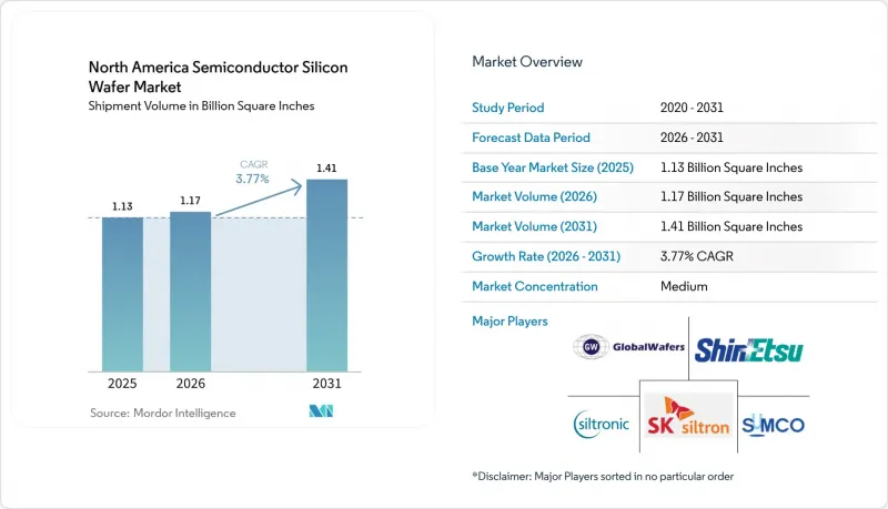
Mordor Intelligence에 의하면, 북미의 반도체 실리콘 웨이퍼 시장 규모(출하량 기반)는 2025년 11억 3,000만 평방인치로 평가되었고, 2026년에는 11억 7,000만 평방인치로 추정되고, 2026-2031년 CAGR 3.77%로 성장을 지속할 전망이며, 2031년에는 14억 1,000만 평방인치에 이를 것으로 예측됩니다.
본 보고서는 웨이퍼 직경별(150mm 이하, 200mm, 300mm), 반도체 소자 유형별(로직, 메모리, 아날로그, 디스크리트 등), 웨이퍼 유형별(프라임 폴리시, 에피택셜, SOI, 특수 실리콘), 최종 사용자별(소비자용 전자기기, 산업용, 통신 등), 국가별로 분류되어 있습니다. 시장 전망은 면적(제곱인치) 기준으로 제시되어 있습니다.
북미의 반도체 실리콘 웨이퍼 시장 동향 및 인사이트
주요 파운드리 업체들의 생산 능력 확대
TSMC, 인텔, 텍사스 기기의 대규모 다년 투자로 인해 북미 반도체 실리콘 웨이퍼 시장이 지속적으로 강화되고 있습니다. 애리조나주의 기가팹 클러스터는 이미 대만과 동등한 수율 수준에 도달했으며, 인텔의 Fab 52는 18A 공정으로 양산을 시작했고, 텍사스 기기는 휴머노이드 로봇을 활용해 셔먼 콤플렉스의 자동화를 실현했습니다. 집중된 수주로 인해 기판 공급업체는 인증 비용을 상각하고 선급금을 확보할 수 있으므로, 예측 가능한 처리량과 노드의 신속한 양산화가 보장됩니다.
미국 'CHIPS법에 따른 인센티브의 급증
직접 보조금, 저리 융자 및 25%의 세액 공제를 통해 폴리실리콘에서 완제품 웨이퍼에 이르는 밸류체인의 모든 단계에서 자본 조달의 장벽이 낮아집니다. 마일스톤에 따른 지급을 통해 투기적인 과잉 건설을 방지하는 한편, 반환 조항이 납세자를 보호합니다. 웨이퍼 제조업체들은 이러한 보조금을 활용해 팹과 같은 부지 내에 거점을 마련함으로써 물류 주기를 단축하고, 북미 반도체 실리콘 웨이퍼 시장공급 탄력성을 강화하고 있습니다.
메모리 시장의 주기적인 침체
범용 DRAM 및 NAND의 지속적인 재고 과잉으로 인해, 2025년에는 클린룸 공간이 소진되었음에도 불구하고 이에 비례한 웨이퍼 수요 증가는 나타나지 않았습니다. 장기 계약 외 가격 하락으로 인해 웨이퍼 공급업체의 이익률이 압박을 받고 있으며, 북미 반도체 실리콘 웨이퍼 시장은 분기마다 급격한 변동에 직면해 있습니다. AI용 고대역폭 메모리가 기여하고 있지만, 재고가 정상화되기 전까지는 수요 부진을 완전히 상쇄할 수는 없습니다.
부문별 분석
북미의 반도체 실리콘 웨이퍼 시장에서 300mm 웨이퍼의 점유율은 수량 기준으로 70.62%를 차지하고 있으며, 최첨단 AI 및 3nm 로직 양산 확대의 혜택을 받고 있습니다. 2031년까지 연평균 성장률(CAGR) 4.95%로 성장할 것으로 전망됩니다. 대형 칩의 GPU, 고밀도 DRAM 및 고도로 자동화된 아날로그 라인은 더 넓은 표면적의 이점을 누리며, 리소그래피 비용을 더 많은 칩에 분산시켜 매출 총이익률을 높이고 있습니다. 따라서 300mm 팹과 관련된 북미 반도체 실리콘 웨이퍼 시장 규모는 전체 시장의 성장 곡선보다 빠른 속도로 확대되고 있어, 공급업체 수요 예측 가능성을 높이고 있습니다.
200mm 웨이퍼는 특히 EV에 탑재되는 양이 급증하고 있어, 자동차, 파워, 그리고 성숙한 아날로그 분야에서 여전히 필수적입니다. 온세미컨덕터와 인피니언의 생산 라인 증산으로 인해 기존 팹은 계속 가동되며, 갑작스러운 노후화를 방지하고 있습니다. 양쪽 직경 모두를 공급하는 업체들은 수요 급감을 완화하고, 기기 세대를 초월한 관계를 심화함으로써 장기적으로 북미 반도체 실리콘 웨이퍼 시장을 강화하고 있습니다.
로직 디바이스는 2025년 출하량의 33.09%를 차지했으며, AI 추론이 스마트폰, PC, 엣지 서버로 이동함에 따라 2031년까지 연평균 성장률(CAGR) 5.25%로 확대될 전망입니다. RibbonFET 및 후면 전류 공급 기술은 트랜지스터의 효율을 높여주지만, 동시에 결정 품질에 대한 요구 사항도 높이고 있습니다. 이 노드들에 웨이퍼를 공급하는 제조업체들은 가격 프리미엄을 확보하고 있으며, 이로 인해 로직 관련 북미 반도체 실리콘 웨이퍼 시장 점유율이 상승하고 있습니다.
메모리 시장의 주기성은 미국의 DRAM 메가팹 건설 발표에도 불구하고, 그 순기여도를 억제하고 있습니다. 대역폭이 높은 메모리 스택은 패키지당 실리콘 사용량이 증가하고 있지만, PC와 휴대전화 수요 부진이 웨이퍼 출하량 전체 증가세를 억제하고 있습니다. 아날로그 및 디스크리트 소자는 꾸준한 한 자릿수 중반대의 출하량 증가세를 보이고 있으며, 산업용 및 통신 분야 고객을 대상으로 하는 기판 공급업체의 포트폴리오 균형을 유지하고 있습니다.
기타 혜택 :
- 엑셀 형식 시장 예측(ME) 시트
- 3개월간의 애널리스트 지원
자주 묻는 질문
목차
제1장 서론
제2장 조사 방법
제3장 주요 요약
제4장 시장 구도
제5장 시장 규모 및 성장 예측
제6장 경쟁 구도
제7장 시장 기회 및 향후 전망
AJY 26.06.22According to Mordor Intelligence, the north america semiconductor silicon wafer market size in terms of shipment volume is expected to grow from 1.13 Billion Square Inches in 2025 to 1.17 Billion Square Inches in 2026 and is forecast to reach 1.41 Billion Square Inches by 2031 at a 3.77% CAGR over 2026-2031.

This report is Segmented by Wafer Diameter (Up To 150mm, 200mm, and 300mm), Semiconductor Device Type (Logic, Memory, Analog, Discrete, and More), Wafer Type (Prime Polished, Epitaxial, SOI, and Specialty Silicon), End-User (Consumer Electronics, Industrial, Telecommunications, and More), and Country. The Market Forecasts are Provided in Terms of Volume (Square Inches).
North America Semiconductor Silicon Wafer Market Trends and Insights
Capacity Expansions by Leading Foundries
Massive multiyear investments from TSMC, Intel, and Texas Instruments continue to upgrade the North America semiconductor silicon wafer market. The Arizona gigafab cluster already matches Taiwan yield levels, Intel's Fab 52 has entered high-volume production on 18A, and Texas Instruments has automated its Sherman complex with humanoid robots. Concentrated orders allow substrate suppliers to amortize qualification costs and lock in advance payments, ensuring predictable throughput and quicker node ramps.
Surge in U.S. CHIPS Act Incentives
Direct grants, low-cost loans, and a 25% tax credit lower capital hurdles for every tier of the value chain, from polysilicon to finished wafers. Milestone-based disbursements prevent speculative overbuilding, while clawback clauses protect taxpayers. Wafer makers leverage these subsidies to co-locate with fabs, shortening logistics cycles and enhancing supply resilience for the North America semiconductor silicon wafer market.
Cyclical Memory Downturns
A persistent inventory overhang in commodity DRAM and NAND used up cleanroom space without proportional wafer pull-through in 2025. Price erosion outside long-term contracts cut margins for wafer suppliers, exposing the North America semiconductor silicon wafer market to sharp quarterly swings. Although high-bandwidth memory for AI helps, it cannot fully neutralize volume softness until inventories normalize.
Other drivers and restraints analyzed in the detailed report include:
- Transition Toward 300 mm Wafers in Logic Nodes
- Rising Demand for Si Power Devices in EVs
- Supply Chain Geographic Concentration Risk
For complete list of drivers and restraints, kindly check the Table Of Contents.
Segment Analysis
The 300 mm slice of the North America semiconductor silicon wafer market stands at 70.62% volume and gains from leading-edge AI and 3 nm logic ramps, and expanding at a 4.95% CAGR through 2031. Large-die GPUs, high-density DRAM, and highly automated analog lines benefit from a larger surface, spreading lithography cost over more die and lifting gross margins. The North America semiconductor silicon wafer market size attached to 300 mm fabs therefore rises faster than the overall curve, reinforcing demand visibility for suppliers.
200 mm wafers remain crucial for automotive, power, and mature analog, particularly as EV content skyrockets. Capacity additions in onsemi and Infineon lines keep legacy fabs busy, preventing sudden obsolescence. Suppliers juggling both diameters offset demand cliffs and deepen relationships across device generations, which strengthens the North America semiconductor silicon wafer market over the long term.
Logic devices held 33.09% of the 2025 volume and are advancing at a 5.25% CAGR to 2031, as AI inference shifts to smartphones, PCs, and edge servers. RibbonFET and backside power delivery sharpen transistor efficiency, but they also raise crystal quality demands. Wafer makers shipping to these nodes capture price premiums, lifting the North America semiconductor silicon wafer market share tied to logic.
Memory's cyclicality tempers its net contribution despite U.S. DRAM megafab announcements. High-bandwidth memory stacks use more silicon per package, yet soft PC and handset demand restrains overall wafer lifts. Analog and discrete devices post steady, mid-single-digit volume growth, balancing the portfolio for substrates suppliers targeting industrial and telecom customers.
List of Companies Covered in this Report:
- Shin-Etsu Chemical Co., Ltd.
- SUMCO Corporation
- GlobalWafers Co., Ltd.
- Siltronic AG
- SK Siltron Co., Ltd.
- Wafer Works Corporation
- Okmetic Oy
- Soitec SA
- Sil'Tronix Silicon Technologies
- SunEdison Semiconductor Ltd.
- Zhonghuan Semiconductor Co., Ltd.
- Simgui Technology Co., Ltd.
- Topsil Semiconductor Materials A/S
- Virginia Semiconductor Inc.
- Addison Engineering, Inc.
- University Wafer, Inc.
- Valley Design Corp.
- Pure Wafer PLC
- NOVA Electronic Materials, LLC
- Wafer World Inc.
Additional Benefits:
- The market estimate (ME) sheet in Excel format
- 3 months of analyst support
TABLE OF CONTENTS
1 INTRODUCTION
- 1.1 Study Assumptions and Market Definition
- 1.2 Scope of the Study
2 RESEARCH METHODOLOGY
3 EXECUTIVE SUMMARY
4 MARKET LANDSCAPE
- 4.1 Market Overview
- 4.2 Market Drivers
- 4.2.1 Soaring Demand for 300 mm Wafers from AI Accelerator Fabs
- 4.2.2 CHIPS Act Incentives Catalyzing Local Wafer Production
- 4.2.3 Rapid Adoption of Electric Vehicles Boosting Power Device Wafers
- 4.2.4 Transition Toward Specialty Silicon for SiC and GaN Devices
- 4.2.5 Miniaturization Roadmap to 2 nm Nodes Requiring Ultra-Flat Prime Wafers
- 4.2.6 Reshoring Initiatives Reducing Supply-Chain Risk
- 4.3 Market Restraints
- 4.3.1 Volatile Polysilicon Prices Squeezing Supplier Margins
- 4.3.2 Lengthy Environmental Permitting Delays for New Fabs
- 4.3.3 Competition from Asian 300 mm Megafabs Limiting Utilization
- 4.3.4 Smartphone Market Slowdown Dampening Legacy Wafer Demand
- 4.4 Industry Value Chain Analysis
- 4.5 Regulatory Landscape
- 4.6 Impact of Macroeconomic Factors on the Market
- 4.7 Technological Outlook
- 4.8 Porter's Five Forces Analysis
- 4.8.1 Bargaining Power of Suppliers
- 4.8.2 Bargaining Power of Buyers
- 4.8.3 Threat of New Entrants
- 4.8.4 Threat of Substitutes
- 4.8.5 Intensity of Competitive Rivalry
5 MARKET SIZE AND GROWTH FORECASTS (VOLUME)
- 5.1 By Wafer Diameter
- 5.1.1 Up to 150 mm
- 5.1.2 200 mm
- 5.1.3 300 mm
- 5.2 By Semiconductor Device Type
- 5.2.1 Logic
- 5.2.2 Memory
- 5.2.3 Analog
- 5.2.4 Discrete
- 5.2.5 Other Semiconductor Device Types (Optoelectronics, Sensors, Micro)
- 5.3 By Wafer Type
- 5.3.1 Prime Polished
- 5.3.2 Epitaxial
- 5.3.3 Silicon-on-Insulator (SOI)
- 5.3.4 Specialty Silicon (High-Resistivity, Power, Sensor-Grade)
- 5.4 By End-user
- 5.4.1 Consumer Electronics
- 5.4.1.1 Mobile and Smartphones
- 5.4.1.2 PCs and Servers
- 5.4.2 Industrial
- 5.4.3 Telecommunications
- 5.4.4 Automotive
- 5.4.5 Other End-user Applications
- 5.4.1 Consumer Electronics
- 5.5 By Country
- 5.5.1 United States
- 5.5.2 Canada
- 5.5.3 Mexico
6 COMPETITIVE LANDSCAPE
- 6.1 Market Concentration
- 6.2 Strategic Moves
- 6.3 Market Share Analysis
- 6.4 Company Profiles (includes Global Level Overview, Market Level Overview, Core Segments, Financials as available, Strategic Information, Market Rank/Share, Products and Services, Recent Developments)
- 6.4.1 Shin-Etsu Chemical Co., Ltd.
- 6.4.2 SUMCO Corporation
- 6.4.3 GlobalWafers Co., Ltd.
- 6.4.4 Siltronic AG
- 6.4.5 SK Siltron Co., Ltd.
- 6.4.6 Wafer Works Corporation
- 6.4.7 Okmetic Oy
- 6.4.8 Soitec SA
- 6.4.9 Sil'Tronix Silicon Technologies
- 6.4.10 SunEdison Semiconductor Ltd.
- 6.4.11 Zhonghuan Semiconductor Co., Ltd.
- 6.4.12 Simgui Technology Co., Ltd.
- 6.4.13 Topsil Semiconductor Materials A/S
- 6.4.14 Virginia Semiconductor Inc.
- 6.4.15 Addison Engineering, Inc.
- 6.4.16 University Wafer, Inc.
- 6.4.17 Valley Design Corp.
- 6.4.18 Pure Wafer PLC
- 6.4.19 NOVA Electronic Materials, LLC
- 6.4.20 Wafer World Inc.
7 MARKET OPPORTUNITIES AND FUTURE OUTLOOK
- 7.1 White-Space and Unmet-Need Assessment
