
|
시장보고서
상품코드
2063398
300mm 실리콘 웨이퍼 : 시장 점유율 분석, 업계 동향 및 통계, 성장 예측(2026-2031년)300mm Silicon Wafer - Market Share Analysis, Industry Trends & Statistics, Growth Forecasts (2026 - 2031) |
||||||
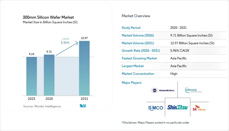
Mordor Intelligence에 의하면, 300mm 실리콘 웨이퍼 시장 규모는 2025년에 91억 9,000만 평방인치로 평가되었습니다. 2026년에 97억 1,000만 평방인치가 되어, 2031년까지 129억 7,000만 평방인치에 이를 것으로 예측됩니다.
2026년부터 2031년까지 연평균 성장률(CAGR) 5.96%로 성장할 것으로 전망됩니다.

본 보고서는 반도체 소자 유형(로직, 메모리, 아날로그, 디스크리트 및 파워, 기타), 웨이퍼 유형(프라임, 폴리시, 에피택셜, 실리콘 온 인슐레이터(SOI), 특수 실리콘), 최종 사용자용도(가전, 산업용, 통신, 자동차, 기타), 지역별로 분류되어 있습니다. 시장 전망은 출하 면적(10억제곱인치) 단위로 제시되어 있습니다.
세계의 300mm 실리콘 웨이퍼 시장 동향 및 분석
첨단 노드의 로직 및 메모리 디바이스에 대한 수요 증가
2nm 및 고대역폭 메모리 라인의 양산화에 따라 웨이퍼 가동 건수가 증가하고 있습니다. 이는 노드의 미세화가 진행될수록 레티클 층이 늘어나고, 결함 허용 범위가 더 엄격해지기 때문입니다. TSMC는 2026년 하반기에 2nm 플랫폼의 양산을 시작하는 것을 목표로 하고 있으며, 칩 1개당 웨이퍼 면적은 3nm 제품에 비해 15% 증가할 것입니다. 마이크론의 HBM4 생산 능력은 2026년까지 포화 상태가 지속될 전망이지만, SK하이닉스는 기존 제품에 비해 50% 더 많은 웨이퍼 표면적을 필요로 하는 12층 적층형 HBM3E의 생산을 확대되고 있습니다. Samsung Electronics는 2026년 말까지 2nm 공정으로 월 2만 1,000장의 웨이퍼 생산을 목표로 하고 있으며, 인텔은 2026년 중반에 외부 고객용 18A 공정의 인증 획득을 목표로 하고 있습니다. 현재 조달 시장에서는 수년에 걸친 기판 공급 계약이 주류를 이루고 있으며, 이로 인해 팹리스 설계 기업에 대한 기존 제조업체의 가격 결정력이 강화되고 있습니다.
아시아태평양의 파운드리 생산 능력 확대
TSMC는 대만, 미국, 일본에 총 1,650억 달러를 투자해 2029년까지 월간 약 120만 장의 300mm 웨이퍼 생산 능력을 추가할 예정입니다. Samsung Electronics는 2030년까지 한국의 메가팹 건설을 위해 300조 원(2,300억 달러)을 투자할 계획입니다. SMIC의 베이징 생산라인은 제조 장비 수출 규제에도 불구하고, 성숙 노드에서월10만 장의 생산을 목표로 하고 있습니다. 100억 유로(113억 달러)의 자금을 바탕으로 유럽 드레스덴에 설립되는 합작 기업은 2027년부터월4만 장의 웨이퍼 생산을 시작할 예정입니다. 웨이퍼 공급업체들은 이러한 거점 근처에 사업장을 두고 있으며, Siltronic이 20억 유로(22억 6,000만 달러)를 투자해 건설 중인 싱가포르 공장이 그 대표적인 예입니다. 에피택셜 블랭크의 리드타임이 최대 18개월까지 길어짐에 따라, 생산 능력을 사전에 확보하는 것이 더욱 중요해지고 있습니다.
300mm 팹용 설비 투자 확대
대당 1억 5,000만-2억 달러에 달하는 EUV 장비 세트의 영향으로, 3nm 이하 신규 시설의 건설 비용은 현재 150억 달러를 초과하고 있습니다. TSMC의 애리조나주 프로젝트 예산은 미국의 인건비 및 인허가 지연으로 인해 400억 달러에서 그보다 더 높은 수준으로 상승했습니다. 인텔의 오하이오주 프로젝트에는 2030년까지 1,000억 달러가 필요할 가능성이 있지만, CHIPS법의 보조금은 총 지출의 고작 한 자릿수 수준만 충당하고 있습니다. 자본 집약도가 높기 때문에 신규 진입은 정부 지원 기업이나 수직 통합형 기업으로 제한되어, 과점적인 시장 구조가 정착되어 있습니다. AI 수요가 부진할 경우, 설비 가동률 하락 위험이 사업자의 대차대조표에 부담을 가중시킬 우려가 있습니다.
부문별 분석
2025년에는 로직 디바이스의 출하 점유율이 43.76%를 차지했으며, 2nm 게이트 올 어라운드(GaA) 트랜지스터의 양산화에 따라 이 점유율은 더욱 상승할 전망입니다. 300mm 실리콘 웨이퍼 시장에서 로직용이 가장 빠르게 성장할 것으로 전망됩니다. 이는 미세화가 진행될수록 레티클 수와 완성된 다이당 웨이퍼 시작 수가 증가하기 때문입니다. 고대역폭 메모리(HBM)가 메모리 시장 점유율을 끌어올리고 있지만, 로직 부문에서는 여전히 수년 단위공급 계약이 주류를 이루고 있어, 이로 인해 주요 파운드리 업체들은 현물 시장공급 부족 영향을 덜 받고 있습니다.
2025년 출하량에서 메모리는 약 35%를 차지하며, HBM의 각 변형 제품은 수직 적층 방식으로 인해 더 많은 면적을 차지했습니다. 아날로그 및 혼합 신호 소자는 약 12%를 차지하며, 수율과 비용 면에서의 이점을 얻기 위해 200mm 공정에서 전환되고 있습니다. 한편, 6%를 차지하는 디스크리트 파워 반도체는 전기차용으로 300mm 웨이퍼로 전환되고 있습니다. 틈새 시장인 광전자공학과 MEMS를 합쳐도 4% 이하에 그치지만, 자동차용 LiDAR와 생체 인식 센서 분야에서 성장세가 두드러지고 있습니다. 따라서 300mm 실리콘 웨이퍼 시장은 로직 반도체의 비중 여하에 따라 영향을 받지만, 폭넓은 다각화를 통해 생산 능력 활용률은 균형을 유지하고 있습니다.
지역별 분석
2025년, 아시아태평양은 출하량의 79.67%를 차지했으며, 대만의 월 300만 장 생산 개시와 한국의 메모리 부문에서의 주도적 입지가 이를 뒷받침하고 있습니다. 치열한 전력 요금 경쟁, 밀집된 공급업체 클러스터, 강력한 정부 지원에 힘입어 이 지역을 중심으로 한 300mm 실리콘 웨이퍼 시장 규모는 2031년까지 연평균 성장률(CAGR) 6.06%로 성장할 전망입니다. 중국에서는 수출 규제가 지속되는 상황에서도 성숙 노드의 확대로 시장 점유율이 확대되고 있습니다. 일본에서는 2조 엔(130억 달러) 규모의 인센티브로 뒷받침되는 구마모토와 Rapidus의 프로그램을 통해 다시 한 번 존재감을 드러내고 있습니다.
북미는 2025년에 약 10%를 차지했으며, CHIPS법에 따른 자금 지원으로 애리조나주, 오하이오주, 아이다호주에서의 건설이 가속화되고 있습니다. 그러나 노동력이나 인허가 관련 장벽으로 인해 아시아에 비해 실현이 더디게 진행되고 있습니다. 유럽은 약 7%를 차지하고 있으며, 430억 유로(486억 달러) 규모의 민관 공동 자금을 통해 2030년까지 전 세계 반도체 생산량의 20%를 달성하겠다는 방침입니다. 높은 에너지 비용과 다양한 규제는 여전히 실행상의 과제로 남아 있습니다.
남미, 중동 및 아프리카의 점유율을 합친 비율은 2025년에 3% 이하에 그쳤습니다. 사우디아라비아와 아랍에미리트(UAE)에서의 자본 프로젝트는 이에 대한 관심이 점차 높아지고 있음을 시사하고 있지만, 확립된 공급망 생태계의 부재로 인해 단기적인 생산량 확대가 제한되고 있습니다. 그 결과, 아시아·태평양 지역공급 차질이 전 세계로 파급되면서, 300mm 실리콘 웨이퍼 시장에서 여전히 지역적 집중 현상이 지속되고 있음을 여실히 드러내고 있습니다.
기타 혜택
- 엑셀 형식 시장 예측(ME) 시트
- 3개월간의 애널리스트 지원
자주 묻는 질문
목차
제1장 서론
제2장 조사 방법
제3장 주요 요약
제4장 시장 구도
제5장 시장 규모 및 성장 예측(지역별 출하량)
제6장 경쟁 구도
제7장 시장 기회 및 향후 전망
KTHAccording to Mordor Intelligence, the 300mm silicon wafer market size is projected to be 9.19 billion square inches in 2025, 9.71 billion square inches in 2026, and reach 12.97 billion square inches by 2031, growing at a 5.96% CAGR from 2026 to 2031.
This report is Segmented by Semiconductor Device Type (Logic, Memory, Analog, Discrete and Power, and More), Wafer Type (Prime Polished, Epitaxial, Silicon-On-Insulator (SOI), and Specialty Silicon), End-User Application (Consumer Electronics, Industrial, Telecommunications, Automotive, and More), and Geography. The Market Forecasts are Provided in Terms of Shipment Area (Billion Square Inches).
Global 300mm Silicon Wafer Market Trends and Insights
Rising Demand For Advanced Node Logic And Memory Devices
Volume ramps at 2-nanometer and high-bandwidth memory lines elevate wafer starts because each node shrink adds reticle layers and tighter defect budgets. TSMC aims for late-2026 volume on its 2 nm platform, consuming 15% more wafer area per chip than 3 nm equivalents. Micron's HBM4 capacity remains fully booked through 2026, while SK Hynix scales 12-high HBM3E stacks that require 50% extra wafer surface versus conventional. Samsung targets 21,000 wafer starts per month at 2 nm by end-2026, and Intel pursues 18A qualification for external customers in mid-2026. Multi-year substrate agreements now dominate procurement, boosting incumbents' pricing leverage over fabless designers.
Expansion Of Foundry Capacities In Asia-Pacific
TSMC has earmarked USD 165 billion across Taiwan, the United States, and Japan, adding roughly 1.2 million monthly 300 mm starts by 2029. Samsung plans KRW 300 trillion (USD 230 billion) for South Korean megafabs through 2030. SMIC's Beijing line seeks 100,000 starts monthly at mature nodes despite tool controls. Europe's Dresden joint venture, backed by EUR 10 billion (USD 11.3 billion), brings 40,000 starts a month beginning 2027. Wafer suppliers co-locate near these hubs, as shown by Siltronic's EUR 2 billion (USD 2.26 billion) Singapore plant. Rising lead times of up to 18 months for epitaxial blanks reinforce capacity pre-commitment.
Escalating Capital Expenditure For 300 mm Fabs
A sub-3 nm greenfield facility now exceeds USD 15 billion, driven by EUV tool sets priced at USD 150 million to USD 200 million apiece. TSMC's Arizona budget rose from USD 40 billion to higher levels because of U.S. labor rates and permitting delays. Intel's Ohio project may need USD 100 billion through 2030, while CHIPS Act subsidies cover only single-digit percentages of total outlays. High capital intensity confines new entry to state-backed or vertically integrated firms, embedding oligopolistic market structure. Should AI demand falter, underutilization risks amplify balance-sheet stress for operators.
Other drivers and restraints analyzed in the detailed report include:
- Proliferation Of AI, HPC And Data-Center Investments
- Adoption Of Backside Power Delivery And 3D IC Packaging
- Supply Chain Vulnerabilities In Polysilicon And Equipment
For complete list of drivers and restraints, kindly check the Table Of Contents.
Segment Analysis
Logic devices controlled 43.76% of shipments in 2025, and this share climbs as 2 nm gate-all-around transistors reach mass production. The 300mm silicon wafer market size allocated to logic is projected to grow fastest because each shrink raises reticle count and wafer starts per finished die. High-bandwidth memory boosts memory's surface share but logic still commands supply contracts that span several years, insulating leading foundries from spot shortages.
Memory held about 35% of 2025 shipments, with HBM variants consuming more area due to vertical stacking. Analog and mixed-signal devices represent roughly 12%, migrating from 200 mm for yield and cost benefits, while discrete power semiconductors at 6% shift to 300 mm to serve electric vehicles. Niche optoelectronics and MEMS together remain below 4% but gain momentum in automotive lidar and biometric sensors. The 300mm silicon wafer market therefore pivots around logic intensity, but broader diversification ensures balanced capacity utilization.
Geography Analysis
Asia-Pacific retained 79.67% of shipments in 2025, anchored by Taiwan's 3 million monthly starts and South Korea's memory leadership. The 300mm silicon wafer market size centered in this region is slated for a 6.06% CAGR through 2031, thanks to competitive electricity rates, dense supplier clusters, and committed public incentives. China's mature-node expansions lift its participation despite ongoing export controls. Japan re-emerges through Kumamoto and Rapidus programs backed by JPY 2 trillion (USD 13.0 billion) incentives.
North America contributed nearly 10% in 2025, with CHIPS Act funding accelerating builds in Arizona, Ohio, and Idaho. However, labor and permitting hurdles slow realization relative to Asia. Europe held roughly 7%, and seeks 20% of global semiconductor output by 2030 via EUR 43 billion (USD 48.6 billion) public-private financingU. Higher energy costs and regulatory diversity remain execution challenges.
South America and the Middle East and Africa together captured less than 3% in 2025. While capital projects in Saudi Arabia and the United Arab Emirates hint at nascent interest, the lack of established supplier ecosystems constrains near-term volume. Consequently, any supply disruption in Asia-Pacific reverberates globally, underscoring persistent regional concentration within the 300mm silicon wafer market.
- SUMCO Corporation
- Shin-Etsu Chemical Co., Ltd.
- GlobalWafers Co., Ltd.
- Siltronic AG
- SK Siltron Co., Ltd.
- Okmetic Oyj
- WaferWorks Corporation
- RS Technologies Co., Ltd.
- ESWIN Materials Co., Ltd.
- Topsil Semiconductor Materials A/S
- LONGi Silicon Materials Corp.
- Gritek Solar Silicon Industry Co., Ltd.
- Poshing Silicon Co., Ltd.
- LX Semicon Co., Ltd.
- Panzhihua Dingxin Electronic Silicon Co., Ltd.
- Jiangsu Zhongneng Silicon Technology Development Co., Ltd.
- PV Crystalox Silicon GmbH
Additional Benefits:
- The market estimate (ME) sheet in Excel format
- 3 months of analyst support
TABLE OF CONTENTS
1 INTRODUCTION
- 1.1 Study Assumptions and Market Definition
- 1.2 Scope of the Study
2 RESEARCH METHODOLOGY
3 EXECUTIVE SUMMARY
4 MARKET LANDSCAPE
- 4.1 Market Overview
- 4.2 Market Drivers
- 4.2.1 Rising Demand for Advanced Node Logic and Memory Devices
- 4.2.2 Expansion of Foundry Capacities in Asia-Pacific
- 4.2.3 Proliferation of AI, HPC, and Data-Center Investments
- 4.2.4 Adoption of Backside Power Delivery and 3D IC Packaging
- 4.2.5 Government Subsidies for Domestic Wafer Supply Chains
- 4.2.6 Heterogeneous Integration Accelerating 300 mm Wafer Utilization
- 4.3 Market Restraints
- 4.3.1 Escalating Capital Expenditure for 300 mm Fabs
- 4.3.2 Supply Chain Vulnerabilities in Polysilicon and Equipment
- 4.3.3 Technical Barriers to Transition Beyond 300 mm Diameter
- 4.3.4 Energy-Intensive Manufacturing Raising Sustainability Concerns
- 4.4 Industry Value Chain Analysis
- 4.5 Regulatory Landscape
- 4.6 Technological Outlook
- 4.7 Impact of Macroeconomic Factors on the Market
- 4.8 Porter's Five Forces Analysis
- 4.8.1 Bargaining Power of Suppliers
- 4.8.2 Bargaining Power of Buyers
- 4.8.3 Threat of New Entrants
- 4.8.4 Threat of Substitutes
- 4.8.5 Competitive Rivalry
5 MARKET SIZE AND GROWTH FORECASTS (SHIPMENT IN AREA)
- 5.1 By Semiconductor Device Type
- 5.1.1 Logic
- 5.1.2 Memory
- 5.1.3 Analog
- 5.1.4 Discrete and Power
- 5.1.5 Other Semiconductor Device Types (Optoelectronics, Sensors, Micro)
- 5.2 By Wafer Type
- 5.2.1 Prime
- 5.2.2 Polished
- 5.2.3 Epitaxial
- 5.2.4 Silicon-on-Insulator (SOI)
- 5.2.5 Specialty Silicon (High-Resistivity, Power, Sensor-Grade)
- 5.3 By End-user Application
- 5.3.1 Consumer Electronics
- 5.3.1.1 Mobile and Smartphones
- 5.3.1.2 PCs and Servers
- 5.3.2 Industrial
- 5.3.3 Telecommunications
- 5.3.4 Automotive
- 5.3.5 Other End-user Applications
- 5.3.1 Consumer Electronics
- 5.4 By Geography
- 5.4.1 North America
- 5.4.1.1 United States
- 5.4.1.2 Canada
- 5.4.1.3 Mexico
- 5.4.2 Europe
- 5.4.2.1 Germany
- 5.4.2.2 United Kingdom
- 5.4.2.3 France
- 5.4.2.4 Rest of Europe
- 5.4.3 Asia-Pacific
- 5.4.3.1 China
- 5.4.3.2 Japan
- 5.4.3.3 India
- 5.4.3.4 South Korea
- 5.4.3.5 Taiwan
- 5.4.3.6 Rest of Asia-Pacific
- 5.4.4 South America
- 5.4.5 Middle East and Africa
- 5.4.1 North America
6 COMPETITIVE LANDSCAPE
- 6.1 Market Concentration
- 6.2 Strategic Moves
- 6.3 Market Share Analysis
- 6.4 Company Profiles (includes Global Level Overview, Market Level Overview, Core Segments, Financials as available, Strategic Information, Market Rank/Share, Products and Services, Recent Developments)
- 6.4.1 SUMCO Corporation
- 6.4.2 Shin-Etsu Chemical Co., Ltd.
- 6.4.3 GlobalWafers Co., Ltd.
- 6.4.4 Siltronic AG
- 6.4.5 SK Siltron Co., Ltd.
- 6.4.6 Okmetic Oyj
- 6.4.7 WaferWorks Corporation
- 6.4.8 RS Technologies Co., Ltd.
- 6.4.9 ESWIN Materials Co., Ltd.
- 6.4.10 Topsil Semiconductor Materials A/S
- 6.4.11 LONGi Silicon Materials Corp.
- 6.4.12 Gritek Solar Silicon Industry Co., Ltd.
- 6.4.13 Poshing Silicon Co., Ltd.
- 6.4.14 LX Semicon Co., Ltd.
- 6.4.15 Panzhihua Dingxin Electronic Silicon Co., Ltd.
- 6.4.16 Jiangsu Zhongneng Silicon Technology Development Co., Ltd.
- 6.4.17 PV Crystalox Silicon GmbH
7 MARKET OPPORTUNITIES AND FUTURE OUTLOOK
- 7.1 White-space and Unmet-Need Assessment
