
|
시장보고서
상품코드
2063401
미국의 반도체 실리콘 웨이퍼 : 시장 점유율 분석, 업계 동향 및 통계, 성장 예측(2026-2031년)United States Semiconductor Silicon Wafer - Market Share Analysis, Industry Trends & Statistics, Growth Forecasts (2026 - 2031) |
||||||
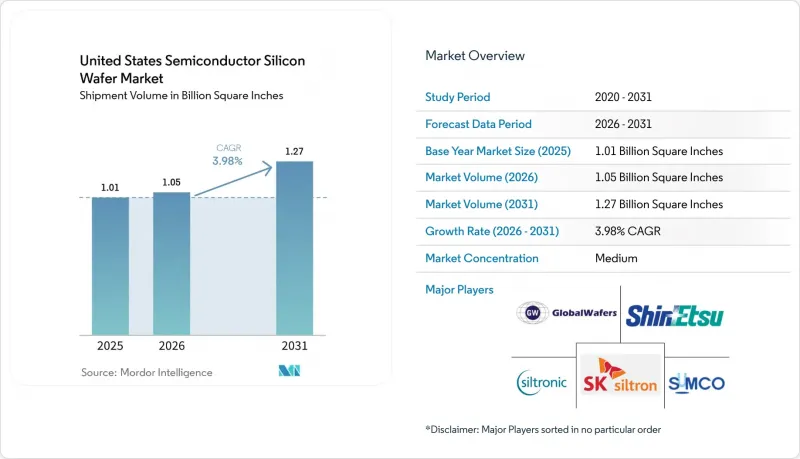
Mordor Intelligence에 의하면, 미국의 반도체 실리콘 웨이퍼 시장 규모(출하량 기반)는 2025년에 10억 1,000만 평방인치로 평가되었습니다. 2026년에는 10억 5,000만 평방인치, 2031년까지 12억 7,000만 평방인치에 이르고, 2026-2031년에 걸쳐 CAGR 3.98%를 나타낼 것으로 예측됩니다.
본 보고서는 웨이퍼 직경(150mm 이하, 200mm, 300mm), 반도체 소자 유형(로직, 메모리, 아날로그, 디스크리트, 기타), 웨이퍼 유형(프라임 연마, 에피택셜, SOI, 특수 실리콘), 최종 사용자(모바일 및 PC 하위 부문을 포함한 가전, 산업용, 통신용, 기타)별로 분류되어 있습니다. 시장 전망은 수량(제곱인치) 기준으로 제시되어 있습니다.
미국의 반도체 실리콘 웨이퍼 시장 동향 및 인사이트
주요 파운드리 업체들의 생산 능력 확대
세계 3대 대기업들의 전례 없는 설비 투자가 미국의 반도체 실리콘 웨이퍼 시장을 재편하고 있습니다. TSMC는 애리조나주에 6개의 메가팹과 2개의 첨단 패키징 라인을 구축했으며, 인텔은 4개 주에 새로운 18A 라인을 증설하고, 삼성은 텍사스주에서 2nm 로직 캠퍼스를 확장하고 있습니다. 각 거점은 본격 가동되면 매년 수백만 장의 300mm 웨이퍼를 소비하게 될 것입니다. 국내 기판 제조업체들은 이러한 수요를 따라잡기 위해 치열한 경쟁을 벌이고 있지만, 새로운 결정 성장 및 슬라이스 공장이 안정적인 생산 능력에 도달하는 것은 2027년 이후가 될 것으로 전망됩니다. 그로 인해 파운드리 각사가 수입에 의존할 수밖에 없는 2년간의 공백기가 발생하게 됩니다.
미국의 ‘CHIPS법’에 따른 인센티브의 급증
'CHIPS·과학법'은 신규 공장 설립의 진입 장벽을 낮춤으로써, 아시아로 향했을 가능성이 있는 투자를 이미 미국으로 전환시켰습니다. 매칭 보조금 덕분에 미국 내 웨이퍼 생산 라인의 실질 비용은 최대 5분의 1까지 절감될 뿐만 아니라, 향후 10년 동안 중국 내 첨단 노드의 확장을 저지하기 위한 엄격한 규제 조치도 포함되어 있습니다. 이러한 조건으로 인해 추가 수요는 국내에 머물게 되지만, 원료인 폴리실리콘은 여전히 독일이나 일본에서 수입되고 있기 때문에 공급 안정성 문제는 부분적으로만 해결된 상황입니다.
메모리 시장의 주기적인 침체
2025년 초, 스마트폰 판매 둔화와 클라우드 기업들의 재고 조정으로 인해 DRAM 및 NAND 공급업체들은 발주량을 대폭 줄였습니다. 메모리용 웨이퍼는 미국의 반도체 실리콘 웨이퍼 시장의 4분의 1 가량을 차지하기 때문에 가격 조정이 한 번만 일어나도 기판 매출액은 급격히 감소합니다. AI 서버용 고대역폭 메모리는 견조한 추세를 유지하고 있지만, 그 틈새 시장은 전반적인 수요를 안정시키기에는 너무 작습니다.
부문별 분석
미국의 반도체 실리콘 웨이퍼 시장에서 300mm 웨이퍼의 점유율은 2025년에 수량 기준으로 70.62%를 나타냈으며, 2031년까지 연평균 성장률(CAGR) 4.95%로 확대될 것으로 전망됩니다. TSMC와 인텔이 애리조나주와 오하이오주에 신설하는 팹만으로도, 풀가동 시 3,000만 제곱인치 이상 수요가 추가될 전망입니다. 웨이퍼당 다이 수가 많으면 비용 효율은 향상되지만, 300mm 실리콘 웨이퍼 생산 능력에서 의미 있는 점유율을 차지하는 세계 공급업체는 단 3곳뿐입니다.
반면, 200mm 기판은 아날로그, MEMS, 자동차용 파워 일렉트로닉스의 기반이 되고 있습니다. 이 형태는 2023년부터 2026년 사이에 14% 확대되었으나, 미국의 생산 능력은 전 세계 공급량의 고작 14%에 불과합니다. 자동차 제조업체들은 2026년부터 2027년에 걸쳐 인버터용 칩과 산업용 제어 칩이 동일한 웨이퍼를 놓고 경쟁하는 상황이 되어, 공급 부족에 직면할 가능성이 있습니다. 150mm 이하 규격은 방위 부문이나 기존 제품 라인에서 여전히 사용되고 있지만, 연간 성장률은 고작 1.8%에 그치고 있어, 웨이퍼 제조업체들이 생산량과 이익률에 상응하는 부문에 투자를 집중해야만 하는 ‘세 가지 속도로 진행되는’ 공급 구조를 더욱 공고히 하고 있습니다.
로직 반도체는 2025년 미국의 반도체 실리콘 웨이퍼 시장 점유율의 33.09%를 차지했으며, 최첨단 노드와 에피택셜 층이 필요한 인공지능(AI) 가속기의 성장에 힘입어 2031년까지 연평균 성장률(CAGR) 5.25%를 나타낼 전망입니다. TSMC는 2025년 하반기 3nm 매출이 스마트폰 매출을 넘어섰다고 밝히며, 고성능 컴퓨팅(HPC) 분야의 성장세를 입증했습니다.
한편, DRAM과 NAND의 가격이 하락함에 따라 2025년 초 메모리 생산량은 감소했습니다. 트레이닝 클러스터용 HBM 장치는 여전히 수익성을 유지하고 있지만, 메모리 웨이퍼 생산량에서 차지하는 비중은 5% 이하에 그치고 있습니다. 200mm 팹에서 아날로그 및 디스크리트 부품은 3-4%의 꾸준한 성장세를 보이고 있으며, 센서와 MEMS 역시 자동차용 레이더 및 스마트 스피커 수요에 힘입어 거의 비슷한 수준의 성장세를 유지하고 있습니다.
기타 혜택
- 엑셀 형식 시장 예측(ME) 시트
- 3개월간의 애널리스트 지원
자주 묻는 질문
목차
제1장 서론
제2장 조사 방법
제3장 주요 요약
제4장 시장 구도
제5장 시장 규모 및 성장 예측
제6장 경쟁 구도
제7장 시장 기회 및 향후 전망
KTHAccording to Mordor Intelligence, the united states semiconductor silicon wafer market size in terms of shipment volume is projected to be 1.01 Billion Square Inches in 2025, 1.05 Billion Square Inches in 2026, and reach 1.27 Billion Square Inches by 2031, growing at a CAGR of 3.98% from 2026 to 2031.

This report is Segmented by Wafer Diameter (Up To 150mm, 200mm, 300mm), Semiconductor Device Type (Logic, Memory, Analog, Discrete, Other), Wafer Type (Prime Polished, Epitaxial, SOI, Specialty Silicon), and End-User (Consumer Electronics With Mobile and PCs Subsegments, Industrial, Telecommunications, and More). The Market Forecasts are Provided in Terms of Volume (Square Inches).
United States Semiconductor Silicon Wafer Market Trends and Insights
Capacity Expansions by Leading Foundries
Unprecedented capital spending by three global leaders is reshaping the United States semiconductor silicon wafer market. TSMC is installing six mega-fabs and two advanced packaging lines in Arizona, Intel is adding new 18A lines across four states, and Samsung is scaling a two-nanometer logic campus in Texas. Each site will consume millions of 300 millimeter wafers every year once fully qualified. Domestic substrate makers are racing to match that pull, but new crystal-growth and slicing workshops will not reach steady output until 2027, which leaves a two-year window in which foundries remain tied to imports.
Surge in U.S. CHIPS Act Incentives
The CHIPS and Science Act lowers the hurdle rate for new plants and has already redirected investments that might have gone to Asia. Matching grants cut the effective cost of a United States wafer line by as much as a fifth and include hard guardrails that block advanced-node expansion in China for a decade. Those terms keep incremental demand local, yet raw polysilicon still arrives from Germany or Japan, meaning supply security is only partially solved.
Cyclical Memory Downturns
DRAM and NAND suppliers cut orders sharply in early 2025 as smartphone sales softened and cloud firms digested inventory. Memory wafers represent nearly one-quarter of the United States semiconductor silicon wafer market, so a single price correction quickly deflates substrate revenue. High-bandwidth memory stays healthy for artificial intelligence servers, but that niche is too small to stabilize overall demand.
Other drivers and restraints analyzed in the detailed report include:
- Transition Toward 300 mm Wafers in Logic Nodes
- Rising Demand for Si Power Devices in EVs
- Supply Chain Geographic Concentration Risk
For complete list of drivers and restraints, kindly check the Table Of Contents.
Segment Analysis
The 300 millimeter slice of the United States semiconductor silicon wafer market size reached 70.62% of volume in 2025 and is forecast to rise at a 4.95% CAGR to 2031. TSMC's and Intel's new Arizona and Ohio fabs alone will add more than 30 million square inches of demand once fully loaded. High die counts per wafer improve cost efficiency, yet only three global suppliers hold a meaningful share of 300 millimeter crystal capacity.
By contrast, 200 millimeter substrates underpin analog, MEMS, and automotive power electronics. That format expanded 14% between 2023 and 2026, but U.S. capacity equals only 14% of global supply. Automakers face a possible shortfall in 2026-2027, when inverter chips will compete with industrial controls for the same wafers. Sub-150 millimeter formats persist in defense and legacy lines but advance just 1.8% a year, reinforcing a three-speed supply picture in which wafer makers must focus investment where volume and margin justify.
Logic captured 33.09% of United States semiconductor silicon wafer market share in 2025 and is tracking a 5.25% CAGR through 2031, propelled by artificial intelligence accelerators that need leading-edge nodes and epitaxial layers. TSMC disclosed that three-nanometer revenue overtook smartphones in late 2025, confirming the momentum behind high-performance computing.
Memory volumes, however, dipped in early 2025 as DRAM and NAND prices softened. Although HBM devices for training clusters stay profitable, they occupy less than 5% of memory wafer volume. Analog and discrete components show steady 3-4% growth in 200 millimeter fabs, while sensors and MEMS stand near the same pace, helped by automotive radar and smart speakers.
List of Companies Covered in this Report:
- Shin-Etsu Chemical Co., Ltd.
- SUMCO Corporation
- GlobalWafers Co., Ltd.
- Siltronic AG
- SK siltron Co., Ltd.
- Okmetic Oy
- Wafer Works Corp.
- Siltronic Silicon Wafer Pte Ltd
- Soitec S.A.
- WaferPro
- Tianjin Zhonghuan Semiconductor Co., Ltd.
- Ultrasil Corporation
- Poshing Technology Co., Ltd.
- Advanced Silicon Technologies
- 300mm Wafer Fab LLC
- Virginia Semiconductor, Inc.
- Rogue Valley Microdevices, Inc.
- SKC Solmics Co., Ltd.
- Qromis, Inc.
- Addison Engineering, Inc.
Additional Benefits:
- The market estimate (ME) sheet in Excel format
- 3 months of analyst support
TABLE OF CONTENTS
1 INTRODUCTION
- 1.1 Study Assumptions and Market Definition
- 1.2 Scope of the Study
2 RESEARCH METHODOLOGY
3 EXECUTIVE SUMMARY
4 MARKET LANDSCAPE
- 4.1 Market Overview
- 4.2 Market Drivers
- 4.2.1 Mainstream, Capacity Expansions by Leading Foundries
- 4.2.2 Mainstream, Surge in U.S. CHIPS Act Incentives
- 4.2.3 Mainstream, Transition Toward 300 mm Wafers in Logic Nodes
- 4.2.4 Mainstream, Rising Demand for Si Power Devices in EVs
- 4.2.5 Under-the-Radar, AI-Optimised SOI Wafer Demand
- 4.2.6 Under-the-Radar, Defense-Grade Radiation-Hard Silicon
- 4.3 Market Restraints
- 4.3.1 Mainstream, Cyclical Memory Downturns
- 4.3.2 Mainstream, Supply Chain Geographic Concentration Risk
- 4.3.3 Under-the-Radar, Crystalline Defect Limits at 3 nm and Below
- 4.3.4 Under-the-Radar, Growing Competition from SiC & GaN Substrates
- 4.4 Industry Value Chain Analysis
- 4.5 Regulatory Landscape
- 4.6 Technology Analysis
- 4.7 Impact of Macroeconomic Factors
- 4.8 Porter's Five Forces Analysis
- 4.8.1 Bargaining Power of Suppliers
- 4.8.2 Bargaining Power of Buyers
- 4.8.3 Threat of New Entrants
- 4.8.4 Threat of Substitutes
- 4.8.5 Intensity of Competitive Rivalry
5 MARKET SIZE AND GROWTH FORECASTS (VOLUME)
- 5.1 By Wafer Diameter
- 5.1.1 Up to 150 mm
- 5.1.2 200 mm
- 5.1.3 300 mm
- 5.2 By Semiconductor Device Type
- 5.2.1 Logic
- 5.2.2 Memory
- 5.2.3 Analog
- 5.2.4 Discrete
- 5.2.5 Other Semiconductor Device Types (Optoelectronics, Sensors, Micro)
- 5.3 By Wafer Type
- 5.3.1 Prime Polished
- 5.3.2 Epitaxial
- 5.3.3 Silicon-on-Insulator (SOI)
- 5.3.4 Specialty Silicon (High-Resistivity, Power, Sensor-Grade)
- 5.4 By End-user
- 5.4.1 Consumer Electronics
- 5.4.1.1 Mobile and Smartphones
- 5.4.1.2 PCs and Servers
- 5.4.2 Industrial
- 5.4.3 Telecommunications
- 5.4.4 Automotive
- 5.4.5 Other End-user
- 5.4.1 Consumer Electronics
6 COMPETITIVE LANDSCAPE
- 6.1 Market Concentration
- 6.2 Strategic Moves
- 6.3 Market Share Analysis
- 6.4 Company Profiles (includes Global Level Overview, Market Level Overview, Core Segments, Financials as available, Strategic Information, Market Rank/Share, Products and Services, Recent Developments)
- 6.4.1 Shin-Etsu Chemical Co., Ltd.
- 6.4.2 SUMCO Corporation
- 6.4.3 GlobalWafers Co., Ltd.
- 6.4.4 Siltronic AG
- 6.4.5 SK siltron Co., Ltd.
- 6.4.6 Okmetic Oy
- 6.4.7 Wafer Works Corp.
- 6.4.8 Siltronic Silicon Wafer Pte Ltd
- 6.4.9 Soitec S.A.
- 6.4.10 WaferPro
- 6.4.11 Tianjin Zhonghuan Semiconductor Co., Ltd.
- 6.4.12 Ultrasil Corporation
- 6.4.13 Poshing Technology Co., Ltd.
- 6.4.14 Advanced Silicon Technologies
- 6.4.15 300mm Wafer Fab LLC
- 6.4.16 Virginia Semiconductor, Inc.
- 6.4.17 Rogue Valley Microdevices, Inc.
- 6.4.18 SKC Solmics Co., Ltd.
- 6.4.19 Qromis, Inc.
- 6.4.20 Addison Engineering, Inc.
7 MARKET OPPORTUNITIES AND FUTURE OUTLOOK
- 7.1 White-space and Unmet-Need Assessment
