
|
시장보고서
상품코드
2063851
미니 LED 칩 시장 : 점유율 분석, 업계 동향과 통계, 성장 예측(2026-2031년)Mini LED Chips - Market Share Analysis, Industry Trends & Statistics, Growth Forecasts (2026 - 2031) |
||||||
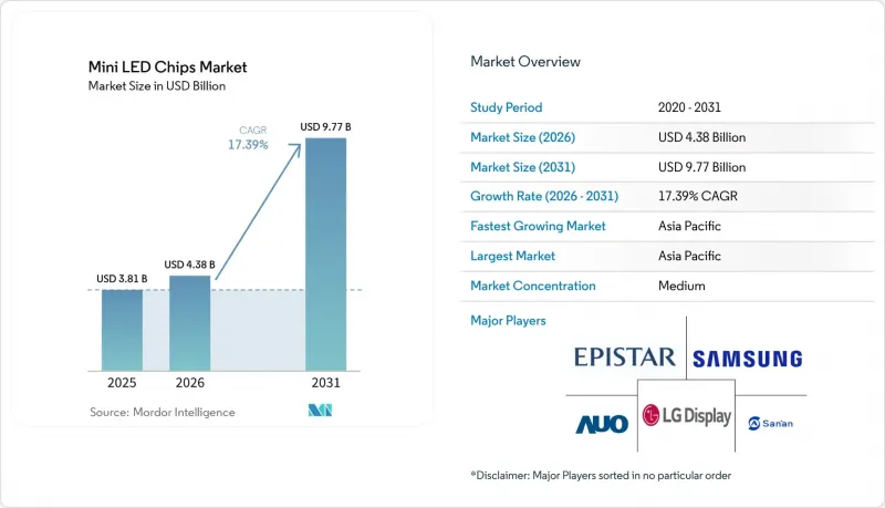
Mordor Intelligence에 의하면, 미니 LED 칩 시장 규모는 2025년 38억 1,000만 달러, 2026년 43억 8,000만 달러에서 2031년까지 97억 7,000만 달러로 확대되어 2026년부터 2031년까지 연평균 복합 성장률(CAGR)은 17.39%를 나타낼 것으로 예측됩니다.
본 보고서는 칩 크기(100-200mm 및 200-300mm), 반도체 소재(GaN/InGaN 및 AlGaInP), 용도(TV용 백라이트, 게이밍 모니터 및 노트북, 태블릿 및 스마트폰, 자동차용 디스플레이, VR/AR 디스플레이 등), 그리고 지역(북미, 유럽, 아시아태평양 등)에 따라 분류되어 있습니다. 시장 전망은 금액(달러) 기준으로 제시되어 있습니다.
세계 미니 LED 칩 시장 동향 및 인사이트
고휘도 HDR TV 패널에 대한 수요 급증
2026년 전시회 현장에서는 최대 20,000개의 로컬 디밍 존과 10,000니트의 최대 밝기를 자랑하는 TV가 다수 전시되면서, 대형 화면에서 발광형 기술의 우위는 상대적으로 약화되고 있었습니다. 중국 브랜드들은 적극적인 판매 지역 확대와 보조금을 통한 가격 경쟁력을 결합함으로써, 2026년 초까지 전 세계 TV 출하량에서 상당한 점유율을 확보했습니다. 삼성은 Neo QLED 라인업을 확대하고, 고휘도를 원하는 소비자를 겨냥한 새로운 미니 LED 제품을 추가함으로써 미국 시장에서 매출 1위 자리를 지켰습니다. 각 패널 제조업체들은 더 큰 화면 크기에서도 밝기를 유지할 수 있도록 열 설계와 밝기 조절 알고리즘을 최적화하고 있습니다. 이러한 변화로 인해, 비용을 비례적으로 늘리지 않고도 구역 수를 늘릴 수 있게 되었습니다. 소비자들이 밝기의 여유를 화질과 동일시하게 되면서, 미니 LED 칩 시장은 선진국과 신흥국 양쪽 지역에서 선순환적인 업그레이드의 혜택을 누리고 있습니다.
웨이퍼 수율 향상을 실현하는 첨단 GaN-on-Si 에피택시
소재 전문 기업과 대량 생산형 LED 제조업체간의 제휴를 통해 200mm GaN-on-silicon 웨이퍼의 상용 생산이 실현되고 있으며, 기판 비용을 절감하는 동시에 한 번의 제조 공정당 다이 수를 늘리고 있습니다. 격자 일치를 갖춘 AlN 버퍼층의 실증을 통해 외부 양자 효율이 30% 이상 향상되었으며, 실리콘 기판에서도 기존에는 사파이어로만 달성 가능했던 밝기 목표를 달성할 수 있음이 입증되었습니다. 파워 디바이스용으로 이미 구축된 파운드리 방식의 툴셋 덕분에 추가 설비 투자가 억제되었으며, 반도체 업계 전체의 미세화 로드맵에 따라 300mm로의 전환을 위한 기반이 마련되었습니다. 웨이크 내 및 웨이크 간의 균일성이 향상됨에 따라, 빈 수율의 경제성이 개선되어 패널 제조업체가 장기적인 비용 절감 궤도를 확립하는 데 도움이 됩니다. 이러한 이점들은 수직 통합 전략을 강화하고, 미니 LED 칩 시장의 실리콘 중심 공급망으로의 전환을 가속화할 것입니다.
OLED 및 신흥 Micro-LED 기술과의 경쟁
애플이 2025년에 발표한 아이패드 프로는 탠덤형 OLED 패널을 탑재해 전체 화면 밝기 1,000니트, 명암비 2,000,000:1을 달성했으며, 이러한 성능은 얇고 가벼운 기기에서 미니 LED의 우위를 깎아내리는 것입니다. OLED 가격 하락은 55형 및 65형 TV 시장에도 파급되고 있으며, 미니 LED 브랜드들은 프리미엄 가격을 유지하기 위해서라도 존 수와 최대 밝기를 높일 수밖에 없는 상황입니다. 한편, 200mm 웨이퍼를 대상으로 한 GaN-on-Si 제휴를 통해 마이크로 LED는 향후 비용 경쟁력을 확보할 전망이며, 예측 기간 내에 기술적 역전극이 일어날 가능성이 높아지고 있습니다. 이러한 두 가지 측면에서의 압박으로 인해 미니 LED가 높은 수익률을 유지할 수 있는 기간이 단축되면서, 특정 프리미엄 부문에서의 성장 기대감이 둔화되고 있습니다. 따라서 공급업체는 시장 점유율을 유지하기 위해 밝기, 수명, 화면 크기와 관련된 가치 제안을 강화해야 합니다.
부문별 분석
2025년, 100-200µm 카테고리는 미니 LED 칩 시장 점유율의 63.40%를 차지하며, 고존 수 TV 및 게이밍 모니터 분야에서 그 입지를 확고히 다졌습니다. 다이 크기가 작아짐에 따라, 세트 제조업체는 주류 패널 크기에 더 많은 로컬 디밍 구역을 집적할 수 있게 되어, 헤일로 현상을 억제하면서도 경쟁력 있는 소매 가격을 유지할 수 있게 됩니다. 그 결과로 발생하는 생산량은 여전히 사파이어 기판과 검증된 매스 트랜스퍼 지그에 유리한 단위 경제성을 뒷받침하고 있습니다. 그러나 패널 구매자들은 더욱 풍부한 명암비를 원한다는 뜻을 밝히며, 공급업체에 존 수를 늘릴 것을 촉구하고 있습니다. 이는 검사 처리량 및 수율 관리에 부담을 주는 요인입니다. 다이 분리 및 사이드월 패시베이션에 대한 지속적인 개선은 점점 더 소형화되는 실적에서 밝기를 유지하는 것을 목표로 하고 있으며, 이를 통해 2031년까지 이 크기 등급의 주류로서의 입지를 공고히할 것입니다.
200-300µm 규모 시장은 연평균 성장률(CAGR) 20.56%로 확대될 것으로 예상되며, 자동차 제조업체와 초대형 TV 제조업체들이 드라이버 아키텍처를 간소화함에 따라 대형 칩 포맷 분야의 미니 LED 칩 시장 규모를 끌어올릴 것으로 보입니다. 존당 다이 수를 줄이고 다이당 밝기를 높임으로써, 실장 시간이 단축되고 드라이버 수가 감소하며, 필러에서 필러까지 이어지는 곡면 콕핏 디스플레이의 열 설계를 용이하게 할 수 있습니다. 또한, 대형 다이(die)는 전류 밀도가 낮기 때문에 자동차 제조업체는 에너지 효율 규제에 대한 여유를 확보할 수 있습니다. 따라서 공급업체들은 다이 수를 줄이는 것과 유리 표면에 칩을 본딩하는 정밀도 사이의 균형을 맞추는 GaN-on-Si 라인에 투자하고 있으며, 이러한 상충 관계로 인해 1m²를 초과하는 디스플레이 영역에서는 여전히 대형 다이가 유리한 것으로 나타납니다. 비용, 신뢰성, 집적화의 장점이 결합되어, 이 크기 등급은 예측 기간이 끝날 때까지 주류 포맷과의 수량 격차를 좁힐 것으로 보입니다.
지역별 분석
2025년, 아시아태평양은 미니 LED 칩 매출의 60.76%를 차지해, 중국의 보조금, 대만의 에피택시 기술, 한국의 패널 투자가 맞물려 자생적인 공급망을 형성함에 따라, 이 지역은 2031년까지 연평균 성장률(CAGR) 21.54%로 성장할 것으로 전망됩니다. 각 부처의 보조금 지원으로 신규 팹의 자본 비용이 절감되는 한편, 선전과 아모이의 클러스터는 대량 전사 및 드라이버 IC 패키징 분야의 학습 주기를 단축하고 있습니다. 대만에서 200mm GaN-on-silicon 에피택시 기술로의 전환은 기존 반도체 인프라를 활용하여, 설비 투자를 비례적으로 늘리지 않고도 생산량을 증가시키고 있습니다. 한국의 주요 디스플레이 제조업체들은 RGB 미니 LED TV 라인업을 확대해 시장 점유율을 지키는 한편, OLED 생산 시설의 규모를 확대해 나가면서 프리미엄 LCD의 차별화를 공고히 하고 있습니다.
북미는 생산량은 적지만, 메가존 백라이트를 채택한 하이엔드 게이밍 모니터와 프리미엄 TV 덕분에 매출액이 두드러지게 높습니다. 삼성, 에이서, 뷰소닉 등의 브랜드는 HDR1000 이상을 지원하는 TV와 디스플레이로 애호가들 수요를 확보하고 있습니다. 소매 분석에 따르면, 소비자들은 특히 교외의 넓은 거실에서 낮 시간대에 TV를 시청할 때, OLED로는 구현할 수 없는 최고 밝기를 원해 미니 LED를 선택하고 있습니다. 자동차 업계의 발전도 이러한 지역 구성을 뒷받침하고 있으며, 디트로이트와 실리콘밸리의 스타트업 기업들은 아시아 공장에서 부품을 조달하면서도 미국의 인포테인먼트 시스템에 맞추어 조정된 곡면 콕핏 패널을 채택하고 있습니다. 규제 측면에서의 역풍은 완만하지만, ‘인플레이션 억제법’에 따른 제조 세액 공제로 인해 드라이버 보드 및 최종 모듈의 현지 조립이 촉진되어, 공급의 일부가 미국으로 이전될 가능성이 있습니다.
유럽 시장 점유율은 다소 낮지만, 에너지 효율을 촉진하는 에코디자인 규제를 통해 기술의 방향성을 결정짓고 있습니다. 독일의 고급 자동차 브랜드들은 밝은 주변 조명 하에서도 가시성 기준을 충족하기 위해 미니 LED 계기판과 승객용 디스플레이를 채택하고 있으며, 이로 인해 대만 및 일본의 모듈 제조업체들과의 제휴가 촉진되고 있습니다. 유럽의 소매업체들은 미니 LED TV가 기존 플라즈마 TV에 비해 1니트당 전력 소비량이 적다는 점을 근거로, 이를 지속 가능한 업그레이드 옵션으로 적극 홍보하고 있습니다. 그러나 전력 가격의 급등으로 인해 디스플레이 교체 주기가 전반적으로 억제되고 있어, 아시아태평양과 비교했을 때 판매 대수 증가세는 완만해지고 있습니다. 의료용 영상 진단 및 방송 스튜디오와 같은 산업 분야에서의 도입은 미니 LED의 안정적인 밝기와 긴 수명을 활용한 새로운 성장의 길을 열어주고 있습니다.
추가적인 장점:
- Excel 형식 시장 예측(ME) 시트
- 3개월간의 애널리스트 지원
자주 묻는 질문
목차
제1장 서론
제2장 조사 방법
제3장 주요 요약
제4장 시장 구도
제5장 시장 규모와 성장 예측
제6장 경쟁 구도
제7장 시장 기회와 향후 전망
JHSAccording to Mordor Intelligence, the mini lED chips market size is projected to expand from USD 3.81 billion in 2025 and USD 4.38 billion in 2026 to USD 9.77 billion by 2031, registering a CAGR of 17.39% between 2026 to 2031.

This report is Segmented by Chip Size (100-200 Mm and 200-300 Mm), Semiconductor Material (GaN/InGaN and AlGaInP), Application (Television Backlighting, Gaming Monitors and Laptops, Tablets and Smartphones, Automotive Displays, VR/AR Displays, and More), and Geography (North America, Europe, Asia Pacific, and More). The Market Forecasts are Provided in Terms of Value (USD).
Global Mini LED Chips Market Trends and Insights
Surging Demand for High-Brightness HDR Television Panels
Trade-show floors in 2026 were crowded with televisions boasting up to 20,000 local-dimming zones and 10,000 nits peak brightness, narrowing the perceived advantage of emissive technologies at premium screen sizes. Chinese brands captured a significant share of global TV unit shipments by early 2026 after pairing aggressive zone counts with subsidy-supported pricing. Samsung retained the top revenue position in the United States by expanding its Neo QLED range and adding new mini-LED SKUs that target brightness-oriented consumers. Panel makers are optimizing thermal architectures and dimming algorithms to sustain brightness across larger diagonals, a shift that amplifies zone counts without proportional cost jumps. As consumers equate luminance headroom with picture quality, the mini LED chips market benefits from a virtuous upgrade cycle across both developed and emerging regions.
Advanced GaN-on-Si Epitaxy Enabling Larger Wafer Yields
Partnerships between materials specialists and high-volume LED manufacturers are bringing 200 mm GaN-on-silicon wafers into commercial production, reducing substrate costs while increasing die counts per run. Demonstrations of lattice-compatible AlN buffer layers delivered external quantum-efficiency gains of more than 30%, validating that silicon substrates can meet brightness targets formerly reserved for sapphire. Foundry-style tool sets already in place for power devices lower incremental capex, creating a glide-path to 300 mm adoption that aligns with broader semiconductor scaling roadmaps. Higher on-wafer and wafer-to-wafer uniformity improves bin-yield economics, helping panel makers lock in long-term cost reduction trajectories. These advantages reinforce vertical integration plays and accelerate the migration of the mini LED chips market toward silicon-centric supply chains.
Competition from OLED and Emerging Micro-LED Technologies
Apple's 2025 iPad Pro launch showed tandem OLED panels hitting 1,000 nits full-screen brightness and a 2,000,000:1 contrast ratio, capabilities that erode mini-LED's advantage in thin-and-light devices. OLED price erosion is cascading into the 55-inch and 65-inch television tiers, forcing mini-LED brands to escalate zone counts and peak luminance just to sustain premiums. Meanwhile, GaN-on-Si partnerships targeting 200 mm wafers position micro-LED for future cost parity, raising the prospect of technological leapfrog within the forecast window. This two-front squeeze shortens the window during which mini-LED can command higher margins, tempering growth expectations in certain premium segments. Vendors must therefore sharpen value propositions around brightness, lifetime, and screen size to defend share.
Other drivers and restraints analyzed in the detailed report include:
- Regional Subsidies Accelerating Mini LED Capacity Build-Out in China
- Rapid Cost Decline in Mass-Transfer Equipment
- High Capital Intensity of Clean-Room Bonding Lines
For complete list of drivers and restraints, kindly check the Table Of Contents.
Segment Analysis
The 100-200 µm category captured 63.40% of the Mini LED Chips market share in 2025, cementing its role in high-zone televisions and gaming monitors. Smaller dice let set makers pack more local-dimming zones into mainstream panel sizes, suppressing halo artifacts while preserving aggressive retail price points. The resulting volumes anchor unit economics that still favor sapphire substrates and proven mass-transfer jigs. Yet panel buyers are signaling appetite for even richer contrast, nudging suppliers toward higher zone counts that strain inspection throughput and yield management. Continuous refinements in die singulation and sidewall passivation aim to sustain brightness at ever-smaller footprints, protecting the mainstream role of this size class through 2031.
The 200-300 µm group is projected to expand at a 20.56% CAGR, lifting the Mini LED Chips market size for larger chip formats as automakers and ultra-large TV vendors simplify driver architectures.Fewer, brighter dice per zone cut placement reduces placement time and driver count, easing thermal design for curved cockpit displays that stretch pillar to pillar. Automotive original equipment manufacturers also gain compliance headroom under energy-efficiency mandates because larger dice operate at lower current density. Suppliers therefore invest in GaN-on-Si lines that balance die-count reduction with chip-on-glass bonding precision, a trade-off that continues to favor larger dice in display areas above 1 m2. The convergence of cost, reliability, and integration advantages positions this size class to narrow the volume gap with mainstream formats by the end of the forecast window.
Geography Analysis
Asia Pacific accounted for 60.76% of mini LED chip revenue in 2025, and the region is forecast to grow at a 21.54% CAGR through 2031 as Chinese subsidies, Taiwanese epitaxy expertise, and Korean panel investments converge into a self-reinforcing supply network. Provincial grants lower capital costs for new fabs, while Shenzhen and Xiamen clusters shorten learning cycles on mass transfer and driver IC packaging. Taiwan's move to 200 mm GaN-on-silicon epitaxy leverages existing semiconductor infrastructure, raising output without proportional tool spend. Korea's display majors defend share by pushing RGB mini-LED TV lineups, anchoring premium LCD differentiation even as they scale OLED fabs.
North America contributes a smaller volume but outsized revenue thanks to high-end gaming monitors and premium televisions that favor mega-zone backlights. Brands such as Samsung, Acer, and ViewSonic capture enthusiast demand with sets and displays certified to HDR1000 and above. Retail analytics show consumers choosing mini-LED for peak brightness that OLED cannot sustain during daytime viewing, especially in large suburban living rooms. Automotive rollouts support the regional mix as Detroit and Silicon Valley startups adopt curved cockpit panels sourced from Asian fabs yet tuned to U.S. infotainment stacks. Regulatory headwinds are mild, but the Inflation Reduction Act's manufacturing credits could spur localized assembly of driver boards and final modules, nudging partial supply migration stateside.
Europe accounts for a modest share but sets technology direction through ecodesign regulations that push energy efficiency. German premium-car brands deploy mini-LED clusters and passenger displays to meet readability standards under bright ambient light, catalyzing partnerships with Taiwanese and Japanese module makers. European retailers promote mini-LED televisions as sustainable upgrades, citing lower power consumption per nit compared to plasma sets being replaced. However, elevated electricity prices temper overall screen-upgrade cycles, moderating unit growth compared with Asia Pacific. Industrial adoption in medical imaging and broadcast studios offers an incremental avenue, leveraging mini-LED's stable luminance and long lifetime.
- Epistar Corporation
- Samsung Electronics Co. Ltd.
- LG Display Co. Ltd.
- AUO Corporation
- San'an Optoelectronics Co. Ltd.
- Nichia Corporation
- Seoul Semiconductor Co. Ltd.
- Osram Opto Semiconductors GmbH
- Cree LED Inc.
- Lumileds Holding B.V.
- PlayNitride Inc.
- Lextar Electronics Corp.
- Innolux Corporation
- TCL Technology Group Corp.
- Vuereal Inc.
- Aledia S.A.
Additional Benefits:
- The market estimate (ME) sheet in Excel format
- 3 months of analyst support
TABLE OF CONTENTS
1 INTRODUCTION
- 1.1 Study Assumptions and Market Definition
- 1.2 Scope of the Study
2 RESEARCH METHODOLOGY
3 EXECUTIVE SUMMARY
4 MARKET LANDSCAPE
- 4.1 Market Overview
- 4.2 Market Drivers
- 4.2.1 Surging Demand for High-Brightness HDR Television Panels
- 4.2.2 Rapid Cost Decline in Mass-Transfer Equipment
- 4.2.3 OEM Preference for Longer-Lifetime Backlights in Gaming Monitors
- 4.2.4 Regulatory Push for Energy-Efficient Automotive Cockpit Displays
- 4.2.5 Advanced GaN-on-Si Epitaxy Enabling Larger Wafer Yields
- 4.2.6 Regional Subsidies Accelerating Mini LED Capacity Build-Out in China
- 4.3 Market Restraints
- 4.3.1 High Capital Intensity of Clean-Room Bonding Lines
- 4.3.2 Competition from OLED and Emerging Micro-LED Technologies
- 4.3.3 Supply-Chain Volatility for Sapphire and Rare-Earth Phosphors
- 4.3.4 Complex Thermal Management Requirements for Dense LED Arrays
- 4.4 Industry Supply-Chain Analysis
- 4.5 Impact of Macroeconomic Factors on the Market
- 4.6 Regulatory Landscape
- 4.7 Technological Outlook
- 4.8 Porter's Five Forces Analysis
- 4.8.1 Threat of New Entrants
- 4.8.2 Bargaining Power of Suppliers
- 4.8.3 Bargaining Power of Buyers
- 4.8.4 Threat of Substitutes
- 4.8.5 Competitive Rivalry
5 MARKET SIZE AND GROWTH FORECASTS (VALUE)
- 5.1 By Chip Size
- 5.1.1 100-200 µm
- 5.1.2 200-300 µm
- 5.2 By Semiconductor Material
- 5.2.1 GaN / InGaN
- 5.2.2 AlGaInP
- 5.3 By Application
- 5.3.1 Television Backlighting
- 5.3.2 Gaming Monitors and Laptops
- 5.3.3 Tablets and Smartphones
- 5.3.4 Automotive Displays (Instrument Cluster, HUD, Infotainment)
- 5.3.5 VR/AR Displays
- 5.3.6 Other Applications (Industrial Displays, Medical Displays)
- 5.4 By Geography
- 5.4.1 North America
- 5.4.2 Europe
- 5.4.3 Asia Pacific
- 5.4.4 South America
- 5.4.5 Middle East and Africa
6 COMPETITIVE LANDSCAPE
- 6.1 Market Concentration
- 6.2 Strategic Moves
- 6.3 Market Share Analysis
- 6.4 Company Profiles (includes Global Level Overview, Market Level Overview, Core Segments, Financials as available, Strategic Information, Market Rank/Share, Products and Services, Recent Developments)
- 6.4.1 Epistar Corporation
- 6.4.2 Samsung Electronics Co. Ltd.
- 6.4.3 LG Display Co. Ltd.
- 6.4.4 AUO Corporation
- 6.4.5 San'an Optoelectronics Co. Ltd.
- 6.4.6 Nichia Corporation
- 6.4.7 Seoul Semiconductor Co. Ltd.
- 6.4.8 Osram Opto Semiconductors GmbH
- 6.4.9 Cree LED Inc.
- 6.4.10 Lumileds Holding B.V.
- 6.4.11 PlayNitride Inc.
- 6.4.12 Lextar Electronics Corp.
- 6.4.13 Innolux Corporation
- 6.4.14 TCL Technology Group Corp.
- 6.4.15 Vuereal Inc.
- 6.4.16 Aledia S.A.
7 MARKET OPPORTUNITIES AND FUTURE OUTLOOK
- 7.1 White-Space and Unmet-Need Assessment
