

|
시장보고서
상품코드
2099411
DRAM 실리콘 웨이퍼 : 시장 점유율 분석, 업계 동향 및 통계, 성장 예측(2026-2031년)DRAM Silicon Wafer - Market Share Analysis, Industry Trends & Statistics, Growth Forecasts (2026 - 2031) |
||||||
 Mordor Intelligence
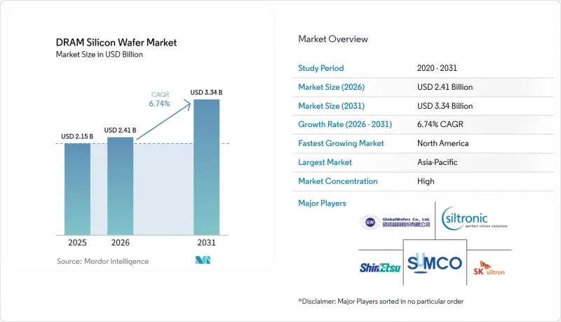
Mordor Intelligence에 의하면, DRAM 실리콘 웨이퍼 시장 규모는 2025년에 21억 5,000만 달러로 평가되었습니다. 2026년 24억 1,000만 달러, 2031년 33억 4,000만 달러에 이를 것으로 예측되며, 2026년부터 2031년에 걸쳐 CAGR 6.74%로 성장할 전망입니다.
본 보고서는 웨이퍼 직경(300mm(12인치), 200mm(8인치), 150mm 미만(6인치 이하)), 웨이퍼 유형(연마 웨이퍼 및 에피택셜(에피) 웨이퍼), DRAM 유형(표준 DRAM, 모바일 DRAM(LPDDR), 그래픽스 DRAM(GDDR), 서버 DRAM 및 특수·자동차용 DRAM), 그리고 지역(북미, 아시아태평양, 기타)별로 분류되어 있습니다. 시장 전망은 금액(달러) 기준으로 제시되어 있습니다.
세계의 DRAM 실리콘 웨이퍼 시장 동향 및 인사이트
HBM 및 첨단 DRAM 노드에 대한 수요 증가
DRAM 실리콘 웨이퍼 시장은 HBM 및 첨단 DRAM 노드에 대한 수요 증가에 힘입어 성장하고 있습니다. 이러한 제품에는 보다 엄격한 공정 제어, 더 균일한 원자재, 그리고 장기간에 걸친 생산 공정을 통해 고품질의 300mm 연마 웨이퍼를 안정적으로 조달할 수 있는 능력이 요구되기 때문입니다. SEMI 보고서에 따르면, 2025년 전 세계 실리콘 웨이퍼 출하량은 5.8% 증가한 1만 2,973 MSI에 달했습니다. 이러한 회복의 주요 요인으로는 HBM 관련 연마 웨이퍼 수요와 로직 관련 첨단 에피택셜 웨이퍼 수요가 꼽힙니다. 이러한 제품 구성은 기판 공급업체에게 중요한 의미를 지닙니다. 첨단 메모리 프로그램이 인증된 생산 능력에서 차지하는 비중이 커지면서, 표준 DRAM 라인에 대한 유연한 배정 여지가 좁아지고 있기 때문입니다. 2026년 5월자 『한국중앙일보』는 수요 둔화 조짐이 보이지 않자 삼성이 평택의 P6 칩 공장 건설을 가속화했다고 보도했습니다. 이는 지역 공급망 전체에서 첨단 메모리 프로그램에 의한 수요가 계속해서 견인하고 있음을 뒷받침하는 것입니다. DRAM 실리콘 웨이퍼 시장에서 인증된 웨이퍼공급량이 여전히 실질적인 제약 요인으로 작용하고 있기 때문에 고객들의 관심은 단순히 팹 가동 수 자체보다는 고품질 기판의 적시 납품에 계속 쏠리고 있습니다.
AI 및 데이터센터용 메모리의 확대
DRAM 실리콘 웨이퍼 시장은 AI 데이터센터 확충의 혜택도 받고 있습니다. 이에 따라 HBM 제품과 대용량 서버 메모리 모두에서 수요가 증가하며, 공급망을 통해 전개되는 웨이퍼 집약형 메모리 프로그램의 수가 늘어나고 있습니다. SEMI의 추산에 따르면, 2026년 프런트엔드 장비에 대한 투자액은 1,330억 달러에 달할 것으로 예상되며, 같은 해 메모리 장비에 대한 투자액만으로도 13% 증가할 것으로 전망되어, 첨단 반도체 생산 능력을 위해 얼마나 막대한 자본이 투입되고 있는지를 보여줍니다. 이러한 투자 패턴은 AI 인프라가 단일 메모리 제품군만을 견인하는 것이 아니라, 웨이퍼 수요, 장비 수요 및 인증 활동에 걸쳐 있는 보다 광범위한 투자 주기를 강화하고 있다는 점에서 중요합니다. 반도체산업협회(SIA)에 따르면, 미국 반도체 기업들은 연간 135억 달러 상당의 실리콘 웨이퍼를 구매하고 있으며, 이 수치는 2029년까지 183억 달러에 달할 것으로 예측됩니다. 이는 향후 반도체 생산에서 기판 공급이 경제적으로 점점 더 중요해지고 있음을 여실히 보여줍니다. DRAM 실리콘 웨이퍼 시장에서는 AI 서버 도입 확대에 따라 표준 연마 완료 웨이퍼부터 더 고도의 기판 등급에 이르기까지 수주 전망이 더욱 명확해지고 있습니다. 이는 메모리 조달이 단일 디바이스 유형에 국한되지 않고 광범위한 범위에 걸쳐 이루어지고 있기 때문입니다.
300mm 웨이퍼 확장의 자본 집약도
DRAM 실리콘 웨이퍼 시장은 여전히 공급 측면에서 엄격한 상한선에 직면해 있습니다. 그 이유는 300mm 웨이퍼 생산 확대에는 막대한 비용이 소요되고, 생산 체제 구축에 수년이 걸리며, 신규 라인이 수익 및 현금 흐름 창출에 완전히 기여하기 전까지 공급업체에 막대한 감가상각비 부담을 안기기 때문입니다. Siltronic사에 따르면, 싱가포르에 신설한 300mm 팹으로 인해 2025년 감가상각비가 3억 4,300만 유로(3억 8,800만 달러) 증가했으며, 매출이 정체되었음에도 불구하고, 연간 EBIT는 마이너스 2,600만 유로(마이너스 2,900만 달러)를 기록했습니다. 이는 새로운 웨이퍼 생산 능력에 대한 투자 회수 주기가 얼마나 장기적인지를 보여줍니다. SUMCO 역시 2026년 1분기에 53억 엔(3,400만 달러)의 영업 손실을 기록했으며, 이러한 압박은 주로 최종 수요의 급락이 아니라 과거 설비 투자에 따른 감가상각비 증가에서 기인한 것이라고 설명했습니다. 따라서 공급업체는 새로운 생산 능력이 상업적으로 수익성을 확보할 때까지 수년에 걸쳐 비용을 흡수해야 하며, 그 결과 신규 투자를 통해 고객에 대한 출하, 가격 책정, 계약 배분의 압박을 완화할 수 있는 속도가 느려집니다. DRAM 실리콘 웨이퍼 시장에서 자본 집약성은 직접적인 제약 요인이 됩니다. 이는 수주 전망이 양호하고 구매자가 장기 계약을 체결할 의사가 있는 경우에도 공급의 신속한 대응을 제한하기 때문입니다.
부문 분석
2025년, 300mm 부문은 DRAM 실리콘 웨이퍼 시장 점유율의 86.43%를 차지하며, 공급망 전체 수요, 투자 계획 및 고객 인증 활동의 중심으로서 확고한 위치를 확립했습니다. 이러한 주도적 지위는 첨단 DRAM 셀이 정밀한 리소그래피, 엄격한 수율 관리, 그리고 성숙한 공정 인프라를 필요로 하기 때문이며, 이러한 요소들은 최첨단 노드에서의 상업적 생산에 있어 300mm 규모에서만 경제성이 확보되기 때문입니다. SUMCO는 2025년 300mm 웨이퍼 수요가 9% 증가했다고 밝히며, 2026년까지도 첨단 DRAM 용도의 성장세가 지속될 것이라고 지적했습니다. 이는 최대 직경 등급이 현재 고객 프로그램에서 여전히 실질적인 중요성을 더해가고 있다는 관점을 뒷받침하는 것입니다. SEMI 보고서에 따르면, 2026년 1분기 전 세계 실리콘 웨이퍼 출하량은 전년 동기 대비 13.1% 증가한 3,275 MSI에 달했으며, 첨단 메모리 및 로직이 회복을 주도하고 있어, 이는 300mm 기판 소비를 뒷받침하는 수요 동향과 밀접하게 일치합니다.
소구경 웨이퍼는 여전히 특수 용도나 레거시 용도로 한정되어 있어, 첨단 DRAM 프로그램에서 대규모 경쟁 상대가 되지 못하며, DRAM 실리콘 웨이퍼 시장의 주요 상업적 가치가 어디에서 창출되는지에 실질적인 변화를 가져오지는 않습니다. Siltronic에 따르면, 2026년 초 현재 AI 관련 용도를 제외한 분야에서 고객사의 재고 수준이 여전히 높은 편이며, 이는 비첨단 웨이퍼 수요 환경이 약세를 보이고 있음을 시사함과 동시에, 첨단 직경과 레거시 직경 간의 경제성 격차가 확대되고 있음을 여실히 드러내고 있습니다. 또한, 이 회사는 2025년에 150mm 이하 웨이퍼를 생산하는 SD 라인을 폐쇄했습니다. 이는 공급업체들이 관련성이 더 높은 기판 등급으로 포트폴리오를 재편하는 과정에서 기존 직경의 생산 능력이 갱신되는 것이 아니라 단계적으로 폐지되고 있음을 뒷받침하는 것입니다. DRAM 실리콘 웨이퍼 시장에서 웨이퍼 직경은 현재 노드 세대를 명확히 나타내는 지표로 기능하고 있습니다. 이는 300mm가 첨단 DRAM과 일치하는 반면, 더 작은 포맷은 이 범주의 주변부에 위치하며 전략적 투자를 거의 유치하지 못하고 있기 때문입니다.
지역별 분석
2025년, 아시아태평양은 DRAM 실리콘 웨이퍼 시장 점유율의 78.64%를 차지했으며, 이 지역은 계속해서 이 부문의 확실한 사업 거점으로서, 기판 공급과 첨단 메모리 제조를 연결하는 주요 통로로서의 지위를 유지했습니다. 한국은 그 중심에 위치해 있으며, Samsung Electronics 및 SK하이닉스가 첨단 DRAM 및 HBM 생산의 세계적 거점을 뒷받침하고 있어, 한국은 다년간의 고객 프로그램을 통해 인증된 웨이퍼 공급을 확보하는 데 있어 매우 중요한 역할을 하고 있습니다. 『한국중앙일보』에 따르면, 삼성의 평택 P5 및 급속도로 건설이 진행 중인 P6 복합 시설은 합쳐서 월 60만 장에 달할 것으로 예상되며, 이는 해당 지역의 메모리 관련 웨이퍼 수요가 더욱 크게 증가할 것임을 시사합니다. 일본도 유사한 공급 경로를 강화하고 있습니다. 신에츠 반도체와 SUMCO가 합쳐서 전 세계 300mm 웨이퍼 생산량의 절반 이상을 공급하고 있으며, 일본의 웨이퍼 생산과 한국의 메모리 생산이 밀접하게 연결되어 이 지역은 상호 의존 관계가 매우 강해지고 있습니다.
북미는 2031년까지 연평균 성장률(CAGR) 8.18%를 나타낼 것으로 예측되며, DRAM 실리콘 웨이퍼 시장에서 가장 성장세가 두드러질 것으로 전망됩니다. 또한, 공급의 현지화가 정책 단계에서 실제 생산 능력으로 전환되고 있는 가장 명확한 사례이기도 합니다. 이러한 변화는 현재 투자 사이클이 시작되기 전까지 미국의 선진적인 상용 300mm 규모에서는 거의 볼 수 없었던, 현지 웨이퍼 공급에 대한 ‘CHIPS법’의 지원에 의해 추진되고 있습니다. NIST에 따르면, GlobalWafers America와 MEMC LLC는 텍사스주 및 미주리주에서 40억 달러 규모의 웨이퍼 투자를 지원하기 위해 최대 4억 600만 달러의 직접 자금을 지원받았습니다. 이를 통해 해당 지역은 국내 웨이퍼 조달을 위한 더욱 견고한 기반을 마련하게 되었습니다. 텍사스주 셔먼에서 진행되는 이 프로젝트는 미국 최초의 첨단 대량 생산형 300mm 실리콘 웨이퍼 공장으로 자리매김하고 있습니다. 이는 메모리 및 로직 분야 고객들을 현지 원자재 공급처에 더 가깝게 만든다는 점에서 중요합니다. 반도체산업협회(SIA)가 2029년까지 미국의 실리콘 웨이퍼 구매액이 183억 달러에 달할 것으로 예측하고 있는 것은 국내 구매자들이 더 광범위하고 탄탄한 공급 기반을 원하고 있는 이유를 설명해 줍니다.
유럽은 신규 그린필드 규모의 생산보다는 특수 등급 웨이퍼 생산 및 공정 연구에 중점을 두고 있으며, 기술적 심도 면에서는 여전히 중요한 역할을 하고 있지만, DRAM 실리콘 웨이퍼 시장에서 단기적인 생산 능력 점유율 확대라는 측면에서는 그다지 중심적인 위치를 차지하고 있지 않습니다. 실트로닉(Siltronic)은 싱가포르 공장이 2025년 8월에 감가상각 기간에 접어들었으며, 2026년 매출은 환율, SD 라인 폐쇄, 그리고 AI 관련 가장 견조한 시장을 제외한 분야의 재고 조정으로 인한 압박에 직면할 것이라고 밝혔습니다. 이는 유럽계 공급업체들이 여전히 선진적인 성장과 부진한 기존 사업 간의 균형을 맞추려 하고 있음을 보여줍니다. 중국도 지역 자급자족을 강화하려 하고 있으며, 『닛케이 아시아』의 보도에 따르면 국내 반도체 제조업체를 대상으로 2026년 말까지 실리콘 웨이퍼의 70% 이상을 중국 공급업체로부터 조달하겠다는 정책 목표가 제시되었습니다. 이는 가격 압박 속에서도 현지 확장 계획을 뒷받침하는 조치입니다. 따라서 DRAM 실리콘 웨이퍼 시장 전체에서 지역적 분포는 아시아 주도의 단일 생산 회랑에서 더 광범위하면서도 여전히 고도로 집중된 구조로 전환되고 있으며, 국내 공급 목표 증가 속도가 인증된 신규 생산 능력의 확대를 앞지르는 양상을 보이고 있습니다.
기타 혜택 :
- 엑셀 형식 시장 예측(ME) 시트
- 3개월간의 애널리스트 지원
자주 묻는 질문
목차
제1장 서론
제2장 조사 방법
제3장 주요 요약
제4장 시장 구도
제5장 시장 규모 및 성장 예측
제6장 경쟁 구도
제7장 시장 기회 및 향후 전망
KTH 26.08.10According to Mordor Intelligence, the DRAM silicon wafer market size is projected to be USD 2.15 billion in 2025, USD 2.41 billion in 2026, and reach USD 3.34 billion by 2031, growing at a CAGR of 6.74% from 2026 to 2031.
This report is Segmented by Wafer Diameter (300mm [12-Inch], 200mm [8-Inch], and Less Than 150mm [6-Inch and Below]), Wafer Type (Polished Wafers, and Epitaxial [Epi] Wafers), DRAM Type (Standard DRAM, Mobile DRAM [LPDDR], Graphics DRAM [GDDR], Server DRAM, and Specialty and Automotive DRAM), and Geography (North America, Asia-Pacific, and More). The Market Forecasts are Provided in Terms of Value (USD).
Global DRAM Silicon Wafer Market Trends and Insights
Rising Demand for HBM And Advanced DRAM Nodes
The DRAM silicon wafer market is being driven by stronger demand for HBM and advanced DRAM nodes, as these products require tighter process control, more consistent starting material, and dependable access to premium 300mm polished wafers across longer production runs. SEMI reported that global silicon wafer shipments rose 5.8% in 2025 to 12,973 MSI, with polished wafer demand linked to HBM and advanced epitaxial wafer demand linked to logic as the main volume drivers behind the recovery. That product split matters for substrate suppliers because advanced memory programs now absorb a larger share of qualified capacity, leaving less room for flexible allocation across standard DRAM lines. Korea JoongAng Daily reported in May 2026 that Samsung accelerated construction of its P6 chip plant in Pyeongtaek because demand showed no sign of easing, which reinforces the continued pull from advanced memory programs across the regional supply chain. In the DRAM silicon wafer market, this keeps customer attention fixed on the timely delivery of high-quality substrates rather than on nominal fab counts alone, because the qualified wafer pool remains the real constraint.
AI and Data Center Memory Expansion
The DRAM silicon wafer market is also benefiting from AI data center build-outs, which are lifting demand across both HBM products and large-capacity server memory, broadening the number of wafer-intensive memory programs moving through the supply chain. SEMI estimated that front-end equipment spending will reach USD 133 billion in 2026, while memory equipment spending alone will rise 13% in the same year, indicating how strongly capital is being directed toward advanced semiconductor capacity. This spending pattern matters because it shows that AI infrastructure is not pulling on only one memory product family, but instead reinforcing a larger investment cycle that spans wafer demand, tool demand, and qualification activity. The Semiconductor Industry Association stated that US chip companies purchase USD 13.5 billion in silicon wafers annually, and that this figure is expected to reach USD 18.3 billion by 2029, highlighting the growing economic weight of substrate availability for future semiconductor output. In the DRAM silicon wafer market, broader AI server deployment supports stronger order visibility across both standard polished wafers and more advanced substrate grades, as memory procurement is broadening rather than narrowing to a single device type.
Capital Intensity of 300mm Wafer Expansion
The DRAM silicon wafer market still faces a hard supply ceiling because 300mm expansion is expensive, takes years to ramp, and burdens suppliers with heavy depreciation before new lines contribute fully to earnings or cash generation. Siltronic said its new 300mm fab in Singapore added EUR 343 million (USD 388 million) to 2025 depreciation, pushing full-year EBIT to EUR -26 million (USD -29 million) even though revenue stayed flat, showing how long the payback cycle can be for new wafer capacity. SUMCO also reported a JPY 5.3 billion (USD 34 million) operating loss in Q1 2026, equivalent to, and tied that pressure mainly to higher depreciation from earlier capital spending rather than to a collapse in end demand. Suppliers therefore absorb years of costs before new output becomes commercially efficient, which slows the pace at which new investment can ease tightness in customer shipments, pricing, and contract allocation. For the DRAM silicon wafer market, capital intensity is a direct restraint because it limits fast supply response even when order visibility is strong, and buyers are willing to commit to longer agreements.
Other drivers and restraints analyzed in the detailed report include:
- 300mm Migration for Memory-Intensive Substrates
- Government Incentives for Domestic Wafer Supply Chains
- Feedstock and High-Purity Polysilicon Dependency
For complete list of drivers and restraints, kindly check the Table Of Contents.
Segment Analysis
The 300mm segment held 86.43% of the DRAM silicon wafer market share in 2025, making it the clear center of demand, investment planning, and customer qualification activity across the supply chain. It leads because advanced DRAM cells require tight lithography, strong yield control, and a mature process infrastructure, which are only economical at the 300mm scale for commercial production at leading nodes. SUMCO said 300mm wafer demand grew 9% in 2025 and pointed to continued momentum in advanced DRAM applications through 2026, which supports the view that the largest-diameter class is still gaining practical importance in current customer programs. SEMI reported that worldwide silicon wafer shipments increased 13.1% year over year in Q1 2026 to 3,275 MSI, with advanced memory and logic leading the recovery, and that aligns closely with the demand profile that favors 300mm substrate consumption.
Smaller diameters remain tied to specialty and legacy uses, so they do not compete at scale for advanced DRAM programs and do not materially alter where the main commercial value of the DRAM silicon wafer market is being created. Siltronic said customer inventories remained elevated outside AI-linked applications in early 2026, indicating weaker conditions for non-advanced wafer demand and underlining the widening gap between advanced and legacy-diameter economics. The company also closed its SD line for wafers up to 150mm in 2025, reinforcing that legacy diameter capacity is being retired rather than renewed as suppliers reshape their portfolios around more relevant substrate classes. In the DRAM silicon wafer market, wafer diameter now works as a clear proxy for node generation because 300mm aligns with advanced DRAM while smaller formats sit at the edge of the category and attract far less strategic investment.
Complete Report Scope:
- By Wafer Diameter
- 300mm (12-inch)
- 200mm (8-inch)
- Less than 150mm (6-inch and below)
- By Wafer Type
- Polished Wafers
- Epitaxial (Epi) Wafers
- By DRAM Type
- Standard DRAM
- Mobile DRAM (LPDDR)
- Graphics DRAM (GDDR)
- Server DRAM
- Specialty and Automotive DRAM
- By Geography
- North America
- Europe
- Asia-Pacific
- China
- Japan
- South Korea
- Taiwan
- Rest of Asia-Pacific
- Rest of the World
Geography Analysis
Asia-Pacific held 78.64% of the DRAM silicon wafer market share in 2025, so the region remained the clear operating center of the category and the main corridor linking substrate supply with advanced memory fabrication. South Korea sits at the core of that position because Samsung Electronics and SK Hynix anchor the global base for advanced DRAM and HBM production, giving the country an outsized role in pulling qualified wafer supply through multi-year customer programs. Korea JoongAng Daily reported that Samsung's Pyeongtaek P5 and fast-tracked P6 complex are expected to reach a combined 600,000 wafers per month, pointing to another large increase in memory-linked substrate demand from the same geography. Japan strengthens the same corridor because Shin-Etsu Handotai and SUMCO together supply more than half of the global 300mm wafer volume, linking Japanese wafer output closely with South Korean memory production and keeping the region highly interdependent.
North America is projected to grow at 8.18% CAGR through 2031, making it the fastest-growing regional slice of the DRAM silicon wafer market and the clearest example of supply localization moving from policy into physical capacity. This shift is being driven by CHIPS Act support for local wafer supply, which had been largely absent at advanced commercial 300mm scale in the United States before the current investment cycle began. NIST said GlobalWafers America and MEMC LLC received up to USD 406 million in direct funding to support USD 4 billion in Texas and Missouri wafer investments, which gives the region a stronger foundation for domestic substrate sourcing. The Sherman, Texas project is positioned as the first advanced high-volume 300mm silicon wafer plant in the United States, which matters because it brings memory and logic customers closer to local starting material supply. The Semiconductor Industry Association's projection that US silicon wafer purchases will reach USD 18.3 billion by 2029 explains why domestic buyers are pushing for a broader and more resilient supply base.
Europe remains more concentrated around specialty-grade wafer production and process research than around new greenfield scale, which keeps it relevant to technology depth but less central to near-term capacity share gains in the DRAM silicon wafer market. Siltronic said its Singapore fab entered depreciation in August 2025 and that 2026 revenue would face pressure from exchange rates, the SD line closure, and inventory corrections outside the strongest AI-linked markets, which shows that European-linked suppliers are still balancing advanced growth with weaker legacy exposure. China is also trying to deepen regional self-sufficiency, with Nikkei Asia reporting a policy target for domestic chipmakers to source more than 70% of their silicon wafers from Chinese suppliers by the end of 2026, which supports local expansion plans even under pricing pressure. Across the DRAM silicon wafer market, geography is therefore shifting from a single Asia-led production corridor toward a broader but still highly concentrated map where domestic supply goals are rising faster than qualified new capacity.
- Shin-Etsu Handotai Co., Ltd.
- SUMCO Corporation
- GlobalWafers Co., Ltd.
- Siltronic AG
- SK Siltron Co., Ltd.
- Soitec S.A.
- Okmetic Oyj
- Wafer Works Corporation
- RS Technologies Co., Ltd.
- Topsil Semiconductor Materials A/S
- Shanghai Simgui Technology Co., Ltd.
- National Silicon Industry Group Co., Ltd.
- GRINM Semiconductor Materials Co., Ltd.
- Zhejiang Jinruihong Technology Co., Ltd.
- Hangzhou Semiconductor Wafer Co., Ltd.
- Zhonghuan Advanced Semiconductor Materials Co., Ltd.
- FST Corporation
Additional Benefits:
- The market estimate (ME) sheet in Excel format
- 3 months of analyst support
TABLE OF CONTENTS
1 INTRODUCTION
- 1.1 Study Assumptions and Market Definition
- 1.2 Scope of the Study
2 RESEARCH METHODOLOGY
3 EXECUTIVE SUMMARY
4 MARKET LANDSCAPE
- 4.1 Market Overview
- 4.2 Market Drivers
- 4.2.1 Rising Demand for HBM and Advanced DRAM Nodes
- 4.2.2 AI and Data Center Memory Expansion
- 4.2.3 300mm Migration for Memory-Intensive Substrates
- 4.2.4 Government Incentives for Domestic Wafer Supply Chains
- 4.2.5 Tight Process Control Requirements for DRAM Yield and Uniformity
- 4.2.6 Supply Localization in Specialty Wafer Flows
- 4.3 Market Restraints
- 4.3.1 Capital Intensity of 300mm Wafer Expansion
- 4.3.2 Feedstock and High-Purity Polysilicon Dependency
- 4.3.3 Qualification Risk and Long Customer Approval Cycles
- 4.3.4 Supply Chain Volatility From Geopolitical Reallocation
- 4.4 Industry Value Chain Analysis
- 4.5 Regulatory Landscape
- 4.6 Technological Outlook
- 4.7 Impact of Macroeconomic Factors on the Market
- 4.8 Porter's Five Forces Analysis
- 4.8.1 Threat of New Entrants
- 4.8.2 Bargaining Power of Buyers
- 4.8.3 Bargaining Power of Suppliers
- 4.8.4 Threat of Substitutes
- 4.8.5 Industry Rivalry
5 MARKET SIZE AND GROWTH FORECASTS (VALUE)
- 5.1 By Wafer Diameter
- 5.1.1 300mm (12-inch)
- 5.1.2 200mm (8-inch)
- 5.1.3 Less than 150mm (6-inch and below)
- 5.2 By Wafer Type
- 5.2.1 Polished Wafers
- 5.2.2 Epitaxial (Epi) Wafers
- 5.3 By DRAM Type
- 5.3.1 Standard DRAM
- 5.3.2 Mobile DRAM (LPDDR)
- 5.3.3 Graphics DRAM (GDDR)
- 5.3.4 Server DRAM
- 5.3.5 Specialty and Automotive DRAM
- 5.4 By Geography
- 5.4.1 North America
- 5.4.2 Europe
- 5.4.3 Asia-Pacific
- 5.4.3.1 China
- 5.4.3.2 Japan
- 5.4.3.3 South Korea
- 5.4.3.4 Taiwan
- 5.4.3.5 Rest of Asia-Pacific
- 5.4.4 Rest of the World
6 COMPETITIVE LANDSCAPE
- 6.1 Market Concentration
- 6.2 Strategic Moves
- 6.3 Market Share Analysis
- 6.4 Company Profiles (includes Global Level Overview, Market Level Overview, Core Segments, Financials as available, Strategic Information, Market Rank/Share, Products and Services, Recent Developments)
- 6.4.1 Shin-Etsu Handotai Co., Ltd.
- 6.4.2 SUMCO Corporation
- 6.4.3 GlobalWafers Co., Ltd.
- 6.4.4 Siltronic AG
- 6.4.5 SK Siltron Co., Ltd.
- 6.4.6 Soitec S.A.
- 6.4.7 Okmetic Oyj
- 6.4.8 Wafer Works Corporation
- 6.4.9 RS Technologies Co., Ltd.
- 6.4.10 Topsil Semiconductor Materials A/S
- 6.4.11 Shanghai Simgui Technology Co., Ltd.
- 6.4.12 National Silicon Industry Group Co., Ltd.
- 6.4.13 GRINM Semiconductor Materials Co., Ltd.
- 6.4.14 Zhejiang Jinruihong Technology Co., Ltd.
- 6.4.15 Hangzhou Semiconductor Wafer Co., Ltd.
- 6.4.16 Zhonghuan Advanced Semiconductor Materials Co., Ltd.
- 6.4.17 FST Corporation
7 MARKET OPPORTUNITIES AND FUTURE OUTLOOK
- 7.1 White-Space and Unmet-Need Assessment


