
|
시장보고서
상품코드
2043994
200mm 실리콘 웨이퍼 : 시장 점유율 분석, 업계 동향 및 통계, 성장 예측(2026-2031년)200mm Silicon Wafer - Market Share Analysis, Industry Trends & Statistics, Growth Forecasts (2026 - 2031) |
||||||
 Mordor Intelligence
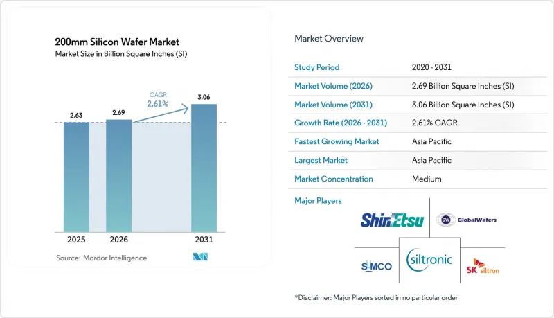
200mm 실리콘 웨이퍼 시장 규모는 2026년에 26억 9,000만 평방인치가 되어, 2031년까지 30억 6,000만 평방인치에 이를 것으로 예측되며, 2026-2031년에 걸쳐 CAGR 2.61%를 나타낼 전망입니다.
자동차의 전동화, 정부 인센티브에 의한 리쇼어링의 가속화, 와이드 밴드갭 디바이스가 더 큰 직경으로 이동함에 따라 성숙한 노드의 생산 능력은 다시금 전략적 중요성을 되찾고 있습니다. 신규 장비보다 40-60% 저렴한 재생 200mm 제조 장비는 이 노드의 비용 우위를 유지하는 한편, 실리콘 카바이드(SiC) 및 질화갈륨(GaN)과 같은 특수 기판은 파워일렉트로닉스 부문에서 그중요성이 더욱 커지고 있습니다. 자동차 및 산업용 공급업체들은 2021-2023년 생산에 영향을 미칠 수 있는 공급 충격을 피하기 위해 200mm 웨이퍼를 장기적으로 확보했으며, 이러한 추세는 향후 10년간 안정적인 가동률을 유지할 수 있는 기반이 될 것으로 보입니다. 한편, Wolfspeed의 300mm SiC의 기술적 혁신은 향후 수익률의 압축을 시사하고 있으며, 200mm 웨이퍼 제조업체들은 수율 향상과 기판 다양화를 통해 자신들의 입지를 지켜야 하는 상황에 처해 있습니다.
세계의 200mm 실리콘 웨이퍼 시장 동향과 인사이트
자동차용 전력반도체 수요 증가
800V 아키텍처를 채택한 전기자동차는 400V 설계에 비해 훨씬 더 큰 SiC와 절연 게이트 바이폴라 트랜지스터(IGBT)의 다이 면적이 필요하기 때문에 대당 웨이퍼 사용량이 증가하여 공급이 부족합니다. STMicroelectronics와 Sanan Optoelectronics는 장기적인 트랙션 인버터 수요를 확보하기 위해 카타니아에 연간 48만 장의 200mm SiC 웨이퍼 생산 능력을 구축하고 있습니다. ON Semiconductor의 20억 달러 규모의 체코 확장 계획도 마찬가지로 EliteSiC 디바이스를 우선시하고 있으며, 이는 Tier 1 공급업체가 순수 다이 비용보다 기판 공급의 안정성을 더 중요하게 여긴다는 것을 보여줍니다. 로옴의 미야자키 공장은 150mm 라인의 1.8배에 달하는 생산능력을 갖추고 있어 일본 국내 조달 체제의 강인함을 높이고 있습니다. 미쓰비시전기가 2026년 4월 구마모토에서 생산을 본격화하면 산업용 모터 드라이브 및 철도 시스템용 200mm SiC 공급이 확대됩니다.
SiC 및 GaN 디바이스의 200mm 플랫폼으로의 전환
보쉬의 로즈빌 공장은 2026년에 200mm SiC를 출하할 계획이며, 이를 통해 결정 성장에서 모듈 패키징까지 수직 통합을 실현할 예정입니다. Infineon의 크림 공장으로의 전환은 에피택셜 수율 문제에 직면했지만, 그럼에도 불구하고 디바이스 비용을 최대 35%까지 절감하여 대면적화에 대한 경제성을 입증했습니다. GaN-on-silicon의 경우, 전 세계 파운드리 업체들이 200mm의 열적 불일치 이점을 활용하여 5G 무선용 전력 증폭기의 허용 오차를 충족시키고 있습니다. 채택이 가속화됨에 따라 10년 단위의 로드맵이 3년 단위의 스프린트(Sprint)로 압축되고, 장비 제조업체와 기판 제조업체는 동시에 규모를 확대해야 하는 상황에 처해 있습니다.
구식 200mm 장비의 부족과 높은 비용
Applied Materials, ASML, Tokyo Electron Ltd.가 10년 이상 전에 신규 200mm 툴세트 출하를 중단했기 때문에 현재 팹 업체들은 재생 장비 입찰을 진행하고 있으며, 그 가격은 2024-2025년에 걸쳐 30% 상승했습니다. 폴라 반도체는 구식 리소그래피 스테퍼를 12개월 동안 기다렸지만, 입고 검사에서 불합격 판정을 받은 출하품의 15%를 폐기해야 했고, 프로젝트 일정과 예산이 지연되는 결과를 초래했습니다. 장비 이력에 대한 낮은 투명성은 거래 위험을 증가시키고 있으며, 특히 예비 부품 공급이 부족한 고밀도 플라즈마 에칭 모듈의 경우 더욱 그러합니다.
부문 분석
2025년 기준, 디스크리트 및 파워 디바이스는 200mm 실리콘 웨이퍼 시장 규모의 30.87%를 차지했으며, 2031년까지 이 부문에서 가장 높은 CAGR(연평균 3.18%)을 기록할 것으로 예측됩니다. 800V 전기자동차 시스템으로의 전환으로 SiC MOSFET과 IGBT의 다이 면적이 확대되어 웨이퍼 수요가 지속적으로 증가하고 있습니다. 로직은 여전히 90nm에서 180nm 노드에 의존하고 있으며, 이 부문에서 200mm는 자본 효율성을 유지하고 있습니다. 한편, NOR 플래시 메모리는 안전성이 매우 중요한 코드 저장 용도에 지속적으로 채택되고 있습니다.
아날로그 IC는 고정밀 수동소자가 300mm에서는 경제적으로 스케일링이 불가능하기 때문에 200mm를 선호합니다. 이에 따라 Texas Instruments는 16억 1,000만 달러의 보조금 중 일부를 200mm 라인의 아날로그 생산능력 증설에 사용하고 있습니다. MEMS 센서와 RF 부품은 광전자에 대한 수요를 증가시키고 있으며, UCI-Express(Universal Chiplet Interconnect Express) 표준은 200mm I/O 다이와 300mm 컴퓨팅 칩렛을 통합할 수 있게 해줍니다. 할 수 있게 되어 하이브리드 수요의 흐름이 생겨나고 있습니다.
"200mm 실리콘 웨이퍼 시장 보고서"는 반도체 소자 유형(로직, 메모리, 아날로그, 디스크리트/파워, 기타), 웨이퍼 유형(프라임 폴리쉬, 에피택셜, 실리콘 온 인슐레이터(SOI), 특수 실리콘), 최종 사용자(가전, 통신, 자동차, 산업, 통신, 자동차, 기타), 지역별로 분류됩니다. 산업용, 통신, 자동차, 기타), 지역별로 분류되어 있습니다. 시장 예측은 출하 면적(10억 평방인치) 단위로 제시되고 있습니다.
지역별 분석
2025년 아시아태평양은 전 세계 200mm 출하량의 79.23%를 차지했습니다. 이는 성숙 노드의 자급자족을 우선시하는 중국의 475억 달러 규모의 '빅펀드 3단계'에 힘입은 것입니다. National Silicon Industry Group과 Zhonghuan Advanced Semiconductor는월5만 웨이퍼 규모의 생산라인을 여러 개 가동하고 있지만, 첨단 제조 장비에 대한 수출 규제로 인해 재생 장비에 의존할 수밖에 없는 상황입니다. 일본의 Shin-Etsu Chemical과 SUMCO는 탄력성(resilience) 확보를 위해 국내 조달을 강력히 요구하는 자동차 산업 고객에 대응하여 200mm 웨이퍼의 생산량을 유연하게 조정하고 있습니다.
북미는 2025년 출하량의 10% 미만을 차지했지만, 'CHIPS법'의 자금이 GlobalWafers, Bosch, Polar Semiconductor에 유입되면서 절대적인 생산능력 증가 속도가 가장 빠를 것으로 예측됩니다. 텍사스 기기(Texas Instruments)의 성숙 노드 증설은 이 지역의 아날로그 및 파워 반도체 생산량을 더욱 증가시켰고, 실트로닉의 포틀랜드 공장은 특수 반도체 수요를 뒷받침하고 있습니다.
유럽의 6-8% 점유율은 현재 EU 칩스법의 지원을 받고 있는 ST마이크로일렉트로닉스의 카타니아 공장과 인피니언의 필라흐 공장이 차지하고 있습니다. 에너지 가격 변동은 여전히 역풍으로 작용하고 있지만, 자동차 제조업체와 산업용 OEM의 현지 조달 의무로 인해 비용 프리미엄이 정당화되었습니다. 남미, 중동, 아프리카를 합쳐도 출하량의 2% 미만에 불과하며, 자국 내 200mm 생산능력이 부족하여 자동차 및 통신 부문은 수입에 의존하고 있습니다.
기타 혜택
- 엑셀 형태 시장 예측(ME) 시트
- 3개월간 애널리스트 지원
자주 묻는 질문
목차
제1장 서론
제2장 조사 방법
제3장 주요 요약
제4장 시장 구도
제5장 시장 규모와 성장 예측(지역별 출하량)
제6장 경쟁 구도
제7장 시장 기회와 향후 전망
KTHThe 200mm silicon wafer market size is projected to be 2.69 billion square inches in 2026 and reach 3.06 billion square inches by 2031, growing at a CAGR of 2.61% from 2026 to 2031. Mature-node capacity is regaining strategic importance as automotive electrification expands, government incentives accelerate reshoring, and wide-bandgap devices shift to larger diameters. Refurbished 200mm tools that cost 40%-60% less than new equipment preserve the node's cost advantage, while specialty substrates such as silicon carbide (SiC) and gallium nitride (GaN) extend its relevance in power electronics. Automotive and industrial suppliers continue locking in long-term 200mm allocations to avoid the supply shocks that upended production between 2021 and 2023, a pattern that supports stable utilization through the decade. At the same time, Wolfspeed's 300mm SiC breakthrough hints at future margin compression, forcing 200mm producers to defend their position through yield improvements and substrate diversification.
Global 200mm Silicon Wafer Market Trends and Insights
Growing Demand for Automotive Power Semiconductors
Electric vehicles that adopt 800 V architectures require significantly larger SiC and insulated-gate bipolar transistor die areas than 400 V designs, lifting wafer starts per vehicle and tightening supply. STMicroelectronics and Sanan Optoelectronics are building capacity for 480,000 200mm SiC wafers per year in Catania to secure long-term traction-inverter demand. ON Semiconductor's USD 2 billion Czech expansion similarly prioritizes EliteSiC devices, illustrating that Tier 1 suppliers are valuing surety of substrate supply over pure die cost. ROHM's Miyazaki plant delivers 1.8 times the output of 150mm lines, bolstering Japan's domestic sourcing resilience. Mitsubishi Electric's April 2026 ramp in Kumamoto extends 200mm SiC supply to industrial motor drives and rail systems.
Migration of SiC and GaN Devices onto 200mm Platforms
Bosch's Roseville facility will ship 200mm SiC in 2026, giving the German firm vertical integration from crystal growth through module packaging. Infineon's Kulim migration encountered epitaxial yield issues but still reduced device cost by up to 35%, validating the economics of larger diameters. For GaN-on-silicon, GlobalFoundries leverages the thermal-mismatch benefits of 200mm to meet 5G radio power-amplifier tolerances. Accelerated adoption compresses a decade-long roadmap into a three-year sprint, forcing equipment makers and substrate growers to scale simultaneously.
Scarcity and High Cost of Legacy 200mm Tools
Applied Materials, ASML, and Tokyo Electron stopped shipping new 200mm toolsets more than a decade ago, so fabs now bid for refurbished equipment where prices climbed 30% between 2024 and 2025. Polar Semiconductor waited 12 months for legacy lithography steppers only to scrap 15% of shipments that failed acceptance tests, pushing project schedules and budgets. Limited transparency on tool pedigree elevates transaction risk, especially for high-density plasma etch modules where spare-part supply is scarce.
Other drivers and restraints analyzed in the detailed report include:
- Government Incentives for Mature-Node Reshoring
- Expansion of IoT and Industrial Sensors
- High-Purity Polysilicon Price Volatility
For complete list of drivers and restraints, kindly check the Table Of Contents.
Segment Analysis
Discrete and power devices represented 30.87% of the 200mm silicon wafer market size in 2025 and will post the segment's best 3.18% CAGR through 2031. The migration of 800 V electric-vehicle systems expands SiC MOSFET and IGBT die areas, translating into sustained wafer demand. Logic remains tied to 90-nm to 180-nm nodes where 200mm retains capital efficiency, while NOR flash memory persists in safety-critical code storage.
Analog ICs favor 200mm because precision passives do not scale economically to 300mm. Texas Instruments is therefore using part of its USD 1.61 billion subsidy for additional analog output on 200mm lines. MEMS sensors and RF components lift optoelectronic demand, and the Universal Chiplet Interconnect Express standard now lets 200mm I/O dies integrate with 300mm compute chiplets, creating a hybrid demand stream.
The 200mm Silicon Wafer Market Report is Segmented by Semiconductor Device Type (Logic, Memory, Analog, Discrete/Power, and More), Wafer Type (Prime Polished, Epitaxial, Silicon-On-Insulator (SOI), and Specialty Silicon), End-User (Consumer Electronics, Industrial, Telecommunications, Automotive, and More), and Geography. The Market Forecasts are Provided in Terms of Shipment Area (Billion Square Inches).
Geography Analysis
Asia-Pacific supplied 79.23% of global 200mm shipments in 2025, fueled by China's USD 47.5 billion Big Fund Phase III that prioritizes mature-node self-sufficiency. National Silicon Industry Group and Zhonghuan Advanced Semiconductor are commissioning multiple 50,000-wafer-per-month lines, although export controls on advanced tools force reliance on refurbished equipment. Japan's Shin-Etsu Chemical and SUMCO adjust 200mm output flexibly, catering to automotive clients that insist on domestic sourcing for resilience.
North America accounted for less than 10% of shipments in 2025 but is on track for the fastest absolute capacity gains as CHIPS Act funds flow to GlobalWafers, Bosch, and Polar Semiconductor. Texas Instruments' mature-node buildout further lifts the region's analog and power output, while Siltronic's Portland plant supports specialty demand.
Europe's 6%-8% share rests on STMicroelectronics' Catania and Infineon's Villach operations, now subsidized under the EU Chips Act. Energy-price volatility remains a headwind, but local sourcing mandates from automakers and industrial OEMs justify the cost premium. South America and the Middle East and Africa collectively represent under 2% of shipments, lacking indigenous 200mm capacity and relying on imports for automotive and telecom sectors.
List of Companies Covered in this Report:
- Shin-Etsu Chemical Co., Ltd.
- SUMCO Corporation
- GlobalWafers Co., Ltd.
- Siltronic AG
- SK Siltron Co., Ltd.
- Wafer Works Corporation
- Soitec SA
- National Silicon Industry Group Co., Ltd.
- Zhonghuan Advanced Semiconductor Materials Co., Ltd.
- Hangzhou Semiconductor Wafer Co., Ltd.
- Okmetic Oyj
- FST Corporation
- GRINM Semiconductor Materials Co., Ltd.
- Zhejiang Jinruihong Technology Co., Ltd.
- Siltronix Group
- WaferTech LLC
- Nova Wafers Inc.
- Freiberger Compound Materials GmbH
- Topsil Semiconductor Materials A/S
Additional Benefits:
- The market estimate (ME) sheet in Excel format
- 3 months of analyst support
TABLE OF CONTENTS
1 INTRODUCTION
- 1.1 Study Assumptions and Market Definition
- 1.2 Scope of the Study
2 RESEARCH METHODOLOGY
3 EXECUTIVE SUMMARY
4 MARKET LANDSCAPE
- 4.1 Market Overview
- 4.2 Market Drivers
- 4.2.1 Growing Demand for Automotive Power Semiconductors
- 4.2.2 Expansion of IoT and Industrial Sensors
- 4.2.3 Government Incentives for Mature-Node Reshoring
- 4.2.4 Migration of SiC and GaN Devices onto 200 mm Platforms
- 4.2.5 Refurbished 200 mm Equipment Deepens Cost Advantage
- 4.2.6 Adoption of 200 mm Wafers in Heterogeneous Chiplet Packaging
- 4.3 Market Restraints
- 4.3.1 Scarcity and High Cost of Legacy 200 mm Tools
- 4.3.2 High-Purity Polysilicon Price Volatility
- 4.3.3 Workforce Knowledge Attrition in Legacy Processes
- 4.3.4 Supply-Chain Concentration Risk in East Asia
- 4.4 Impact of Macroeconomic Factors on the Market
- 4.5 Industry Value Chain Analysis
- 4.6 Regulatory Landscape
- 4.7 Technological Outlook
- 4.8 Porter's Five Forces Analysis
- 4.8.1 Threat of New Entrants
- 4.8.2 Bargaining Power of Suppliers
- 4.8.3 Bargaining Power of Buyers
- 4.8.4 Threat of Substitutes
- 4.8.5 Competitive Rivalry
5 MARKET SIZE AND GROWTH FORECASTS (SHIPMENT IN AREA)
- 5.1 By Semiconductor Device Type
- 5.1.1 Logic
- 5.1.2 Memory
- 5.1.3 Analog
- 5.1.4 Discrete/Power
- 5.1.5 Other Semiconductor Device Types (Optoelectronics, Sensors, Micro)
- 5.2 By Wafer Type
- 5.2.1 Prime Polished
- 5.2.2 Epitaxial
- 5.2.3 Silicon-on-Insulator (SOI)
- 5.2.4 Specialty Silicon (High-Resistivity, Power, Sensor-Grade)
- 5.3 By End-User Application
- 5.3.1 Consumer Electronics
- 5.3.1.1 Mobile and Smartphones
- 5.3.1.2 PCs and Servers
- 5.3.2 Industrial
- 5.3.3 Telecommunications
- 5.3.4 Automotive
- 5.3.5 Other End-User Applications
- 5.3.1 Consumer Electronics
- 5.4 By Geography
- 5.4.1 North America
- 5.4.1.1 United States
- 5.4.1.2 Canada
- 5.4.1.3 Mexico
- 5.4.2 Europe
- 5.4.2.1 Germany
- 5.4.2.2 United Kingdom
- 5.4.2.3 France
- 5.4.2.4 Rest of Europe
- 5.4.3 Asia-Pacific
- 5.4.3.1 China
- 5.4.3.2 Japan
- 5.4.3.3 India
- 5.4.3.4 South Korea
- 5.4.3.5 Taiwan
- 5.4.3.6 Rest of Asia-Pacific
- 5.4.4 South America
- 5.4.5 Middle East and Africa
- 5.4.1 North America
6 COMPETITIVE LANDSCAPE
- 6.1 Market Concentration
- 6.2 Strategic Moves
- 6.3 Market Share Analysis
- 6.4 Company Profiles (includes Global Level Overview, Market Level Overview, Core Segments, Financials as available, Strategic Information, Market Rank/Share, Products and Services, Recent Developments)
- 6.4.1 Shin-Etsu Chemical Co., Ltd.
- 6.4.2 SUMCO Corporation
- 6.4.3 GlobalWafers Co., Ltd.
- 6.4.4 Siltronic AG
- 6.4.5 SK Siltron Co., Ltd.
- 6.4.6 Wafer Works Corporation
- 6.4.7 Soitec SA
- 6.4.8 National Silicon Industry Group Co., Ltd.
- 6.4.9 Zhonghuan Advanced Semiconductor Materials Co., Ltd.
- 6.4.10 Hangzhou Semiconductor Wafer Co., Ltd.
- 6.4.11 Okmetic Oyj
- 6.4.12 FST Corporation
- 6.4.13 GRINM Semiconductor Materials Co., Ltd.
- 6.4.14 Zhejiang Jinruihong Technology Co., Ltd.
- 6.4.15 Siltronix Group
- 6.4.16 WaferTech LLC
- 6.4.17 Nova Wafers Inc.
- 6.4.18 Freiberger Compound Materials GmbH
- 6.4.19 Topsil Semiconductor Materials A/S
7 MARKET OPPORTUNITIES AND FUTURE OUTLOOK
- 7.1 White-Space and Unmet-Need Assessment