|
시장보고서
상품코드
2043996
독일의 반도체 실리콘 웨이퍼 : 시장 점유율 분석, 업계 동향 및 통계, 성장 예측(2026-2031년)Germany Semiconductor Silicon Wafer - Market Share Analysis, Industry Trends & Statistics, Growth Forecasts (2026 - 2031) |
||||||
 Mordor Intelligence
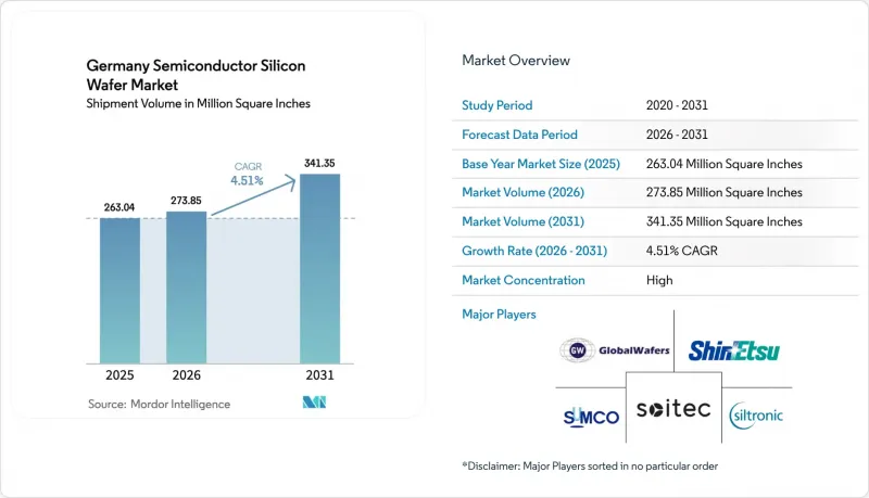
독일의 반도체 실리콘 웨이퍼 시장 규모(출하량 기반)는 2025년에 2억 6,304만 평방인치로 평가되었습니다. 2026년 2억 7,385만 평방인치에서 2031년까지 3억 4,135만 평방인치에 이를 것으로 예상되며, 예측 기간 CAGR은 4.51%를 나타낼 전망입니다..
(2026-2031년).
인텔, TSMC, Infineon, 세계 파운드리를 중심으로 한 300mm 로직 및 파워 디바이스용 팹의 다년간의 확대로 인해 프라임 연마 및 에피택셜 기판에 대한 장기적인 수요가 증가하고 있는 반면, 계약 가격은 타이트해지고 있습니다. 풍력 및 태양광 발전 관련 기업의 전력 구매 계약으로 아시아 지역과의 역사적인 에너지 비용 격차가 줄어들고 있으며, 독일의 반도체 실리콘 웨이퍼 시장의 경쟁이 강화되고 있습니다. 양자 기술용 플로트존 고순도 웨이퍼와 자동차 레이더용 완전 공핍형 SOI로의 전환이 특수 용도 부문의 성장을 견인하고 있습니다. 한편, 폴리실리콘 가격 변동과 산업용 관세의 고공행진으로 인해 단기 수익률은 계속 압박을 받고 있으며, 생산자들은 고부가가치 부문과 장기 인수 계약을 우선시할 수밖에 없는 상황에 처해 있습니다.
독일의 반도체 웨이퍼 시장 동향과 인사이트
독일 300mm 팹 확장을 위한 견조한 설비 투자 계획
인텔은 2028년 생산 개시 시점에 5nm 이하 로직 생산 능력을 제공할 300억 유로(3400억 달러) 규모의 투자 계획의 일환으로 2025년 중반에 맥데부르크에 두 개의 팹을 착공했습니다. TSMC, Bosch, Infineon, NXP는 공동으로 드레스덴에 'European Semiconductor Manufacturing Company'를 설립했습니다. 이는 100억 유로(113억 달러) 규모의 프로젝트로, 2027년까지 28nm, 22nm, 16nm 공정으로월4만장의 웨이퍼를 생산할 예정입니다. 인피니언이 2025년 초에 파일럿 생산을 시작한 50억 유로(57억 달러) 규모의 '스마트 파워 팹(Smart Power Fab)'은 300mm 라인에서 실리콘 카바이드와 고전압 실리콘을 생산하는 것을 목표로 하고 있습니다. 세계파운드리는 2028년 완료되는 11억 유로(12억 5,000만 달러) 규모의 확장 계획을 통해 드레스덴 공장의 연간 300mm 웨이퍼 생산능력을 100만장 이상 확대할 예정입니다. 이 프로젝트들은 대체로 연마된 웨이퍼의 리드타임을 단축하고, 시장의 장기적인 성장 궤도를 뒷받침하는 다년간의 인수 계약을 확보하기 위한 것입니다.
2025년 이후 자동차 칩 수요 회복 전망
독일의 자동차 생산량은 2024년 410만대로 회복되고, 2022-2023년 재고 조정기에 침체되었던 칩 주문이 회복되었습니다. 인피니언은 2025년도에 전기자동차(EV) 구동계용 파워 디바이스 출하량이 두 자릿수 성장을 기록했으며, Porsche, Tycan 등의 양산 모델에서 실리콘 카바이드(SiC) MOSFET이 실리콘 IGBT 대비 3%의 효율 향상을 실현하고 있다고 보고했습니다. 도핑 변동률이 2% 이하인 고전압 에피택셜 웨이퍼를 필요로 하는 800V 배터리 시스템으로의 전환이 수요를 촉진하고 있습니다. 2025년 시행되는 유로7 규제는 1대당 여러 개의 센서와 마이크로컨트롤러를 의무화하여 웨이퍼의 필요 수량을 더욱 증가시킬 것입니다. 자동차 제조업체가 공급을 확보함에 따라 웨이퍼 판매업체는 장기 계약과 엄격한 사양으로 인한 프리미엄 가격의 혜택을 누리고 있습니다.
변동이 심한 폴리실리콘 가격
중국 공급업체들이 연간 40만 톤의 생산능력을 증설함에 따라 반도체 폴리실리콘 가격은 2022년 초 1kg당 35달러에서 2024년 12월까지 1kg당 6.5달러로 급락했습니다. 실트로닉은 2025년 상반기 원자재 비용이 12% 하락했지만, 현물 가격은 여전히 장기 계약의 하한가보다 40% 낮게 형성되어 있어 투자 계획의 불확실성을 초래하고 있다고 경고했습니다. 만약 가격이 20달러/kg으로 빠르게 회복된다면, 디바이스 제조업체가 가격 인상을 받아들이지 않는 한 웨이퍼 제조업체의 이익률은 3-5% 하락할 것입니다. 이러한 불확실성으로 인해 중소업체들은 새로운 초크랄스키법 인양장비 도입을 주저하고 있으며, 그 결과 원료를 자체적으로 정제하는 수직계열화 경쟁업체들 시장 점유율 통합이 진행되고 있습니다. 가격이 안정될 때까지 공급 기반은 증산에 대해 신중한 태도를 유지할 것으로 보입니다.
부문 분석
2025년 독일의 반도체 실리콘 웨이퍼 시장에서 300mm 웨이퍼는 74.68%의 압도적인 출하 점유율을 기록하며 다른 모든 직경의 웨이퍼를 앞질렀습니다. 최첨단 로직 및 자동차용 파워 디바이스용 제조 장비는 이 형태를 중심으로 표준화되어 있으며, 200mm 대체품에 비해 2배 이상의 유효 다이 면적을 제공하여 칩당 가공 비용을 약 30% 절감할 수 있습니다. 인텔의 맥데부르크 공장에서는 사이트 평탄도 0.08마이크로미터 이하, 총 두께 변동 0.15마이크로미터 이하의 사양을 요구하고 있으며, 이 때문에 인증 벤더 리스트는 Shin-Etsu Chemical과 SUMCO의 프리미엄 그레이드에 한정되어 있습니다.
2025년에는 결정 인출 리드타임이 24개월에 달하고, 300mm 프라임 연마 웨이퍼의 계약 가격이 전년 대비 한 자릿수 초반에서 중반까지 상승했습니다. 200mm급은 아날로그, MEMS, 디스크리트 제조에서 전략적 중요성을 유지하고 있습니다. 200mm 전용인 X-FAB의 에어플트 라인은 다이 사이즈가 10mm2를 초과하는 산업용 센서 수요를 충족시키고 있습니다. 직경 150mm 미만은 주로 레거시 옵토일렉트로닉스에 국한되어 있으며, 공급업체들이 구형 용광로를 합리화함에 따라 생산 능력은 더욱 통합될 것으로 예측됩니다.
2025년 출하량 중 로직 웨이퍼가 36.82%를 차지했으며, 이는 독일이 엣지 AI 컨트롤러와 통합 자동차 도메인 프로세서로 전환하고 있음을 반영합니다. TSMC의 드레스덴 공장에서만 28nm, 22nm, 16nm 공정으로월4만장의 300mm 웨이퍼를 처리할 예정으로, 이는 프라임 폴리싱 공급에 대한 로직 수요의 견인력을 확고히할 것입니다. 독일 내 DRAM과 NAND의 프론트엔드 생산능력은 제한적이기 때문에 메모리 부문의 점유율은 여전히 작지만, 데이터센터의 성장과 함께 특수 메모리 부문의 제휴에 대한 신중한 관심이 높아지고 있습니다.
산업용 센서 어레이에 필수적인 아날로그 및 혼합 신호 장치는 인더스트리 4.0의 확산에 힘입어 웨이퍼 생산량의 5분의 1 이상을 차지했습니다. EV 구동계용 실리콘 카바이드 MOSFET을 포함한 개별 부품과 전력 부품은 높은 단가를 실현하여 제조업체들이 가전제품의 수익률 하락을 상쇄하는 데 도움을 주고 있습니다. 완전 공핍형 SOI 플랫폼에서 로직과 아날로그의 융합은 디바이스 유형의 경계를 더욱 모호하게 만들고, 프로세스 흐름의 유연성을 높입니다.
"독일의 반도체 실리콘 웨이퍼 시장 보고서'는 웨이퍼 직경(150mm 이하, 200mm, 300mm), 반도체 디바이스 유형(로직, 메모리, 아날로그, 디스크리트, 기타), 웨이퍼 유형(프라임 폴리쉬, 에피택셜, 실리콘 온 인슐레이터(SOI), 특수 실리콘), 최종 사용자(PC, 서버, 통신, 자동차, 통신, 자동차, 기타)로 분류하여 분석하였습니다. SOI), 특수 실리콘), 최종 사용자(PC 및 서버, 통신, 자동차, 기타)로 분류되어 있습니다. 시장 예측은 출하량(평방인치) 기준으로 제공됩니다.
기타 혜택
- 엑셀 형태 시장 예측(ME) 시트
- 3개월간 애널리스트 지원
자주 묻는 질문
목차
제1장 서론
제2장 조사 방법
제3장 주요 요약
제4장 시장 구도
제5장 시장 규모와 성장 예측
제6장 경쟁 구도
제7장 시장 기회와 향후 전망
KTHThe Germany semiconductor silicon wafer market size in terms of shipment volume was valued at 263.04 Million Square Inches in 2025 and is estimated to grow from 273.85 Million Square Inches in 2026 to reach 341.35 Million Square Inches by 2031, at a CAGR of 4.51% during the forecast period (2026-2031).
A multi-year build-out of 300 mm logic and power-device fabs, anchored by Intel, TSMC, Infineon, and GlobalFoundries, is lifting long-term demand for prime polished and epitaxial substrates while tightening contract pricing. Corporate power-purchase agreements for wind and solar electricity are beginning to close the historical energy-cost gap with Asia, strengthening the competitiveness of Germany's semiconductor silicon wafer market. Parallel shifts toward float-zone high-purity wafers for quantum initiatives and fully depleted SOI for automotive radar add specialty upside. At the same time, volatile polysilicon pricing and elevated industrial tariffs keep near-term margins under pressure, compelling producers to prioritize high-value segments and long-term offtake contracts.
Germany Semiconductor Silicon Wafer Market Trends and Insights
Strong Capex Pipeline for 300 Mm Fab Expansions in Germany
Intel broke ground on two Magdeburg fabs in mid-2025 as part of a EUR 30 billion (USD 34 billion) commitment that will deliver sub-5 nm logic capacity when production starts in 2028. TSMC, Bosch, Infineon, and NXP jointly launched the European Semiconductor Manufacturing Company in Dresden, a EUR 10 billion (USD 11.3 billion) venture slated to produce 40,000 wafers per month at 28 nm, 22 nm, and 16 nm nodes by 2027. Infineon's EUR 5 billion (USD 5.7 billion) Smart Power Fab, which entered pilot output in early 2025, targets silicon carbide and high-voltage silicon on 300 mm lines. GlobalFoundries is adding more than 1 million 300 mm wafers per year to its Dresden plant through a EUR 1.1 billion (USD 1.25 billion) expansion that was completed in 2028. Collectively, these projects compress polished-wafer lead times and secure multi-year offtake agreements that underpin the market's long-term growth trajectory.
Revival of Automotive Chip Demand Post-2025
German vehicle output rebounded to 4.1 million units in 2024, restoring chip orders that had stalled during the 2022-2023 inventory correction. Infineon reported double-digit growth in power-device shipments for electric-vehicle drivetrains during fiscal 2025, with silicon carbide MOSFETs delivering 3% efficiency gains over silicon IGBTs in production models such as the Porsche Taycan. Demand is reinforced by the shift to 800 V battery systems that require high-voltage epitaxial wafers with sub-2% doping variation. Euro 7 rules, effective 2025, require multiple sensors and microcontrollers per car, further increasing wafer volume requirements. As automakers lock in supply, wafer sellers benefit from longer contracts and tighter specification premiums.
Volatile Polysilicon Pricing
Semiconductor-grade polysilicon plunged from USD 35 kg-1 in early 2022 to USD 6.5 kg-1 by December 2024 after Chinese suppliers added 400,000 t of annual capacity. Siltronic said raw-material costs fell 12% in H1 2025 but warned that spot quotes remain 40% beneath long-term contract floors, clouding investment planning. A rapid rebound toward USD 20 kg-1 would slice 3-5 percentage points from wafer-maker margins unless device customers accept price increases. The unpredictability deters smaller producers from green-lighting new Czochralski pullers, effectively consolidating share with vertically integrated rivals that refine their own feedstock. Until pricing stabilizes, the supply base will stay cautious on incremental capacity.
Other drivers and restraints analyzed in the detailed report include:
- EU Chips Act Incentives for On-Shore Wafer Production
- Increasing Adoption of Power Devices for E-Mobility
- High Energy Costs Versus Asian Peers
For complete list of drivers and restraints, kindly check the Table Of Contents.
Segment Analysis
The Germany semiconductor silicon wafer market recorded 300 mm substrates at a commanding 74.68% volume share in 2025, outstripping all other diameters. Tooling for leading-edge logic and automotive power devices is standardized around this format, which delivers more than twice the usable die area of 200 mm alternatives, trimming per-chip processing cost by roughly 30%. Intel's Magdeburg fabs impose site-flatness below 0.08 µm and total-thickness variation under 0.15 µm, specifications that narrow the approved-vendor list to Shin-Etsu and SUMCO's premium grades.
Contract prices for 300 mm prime-polished wafers rose to low-to-mid single digits year over year in 2025 as crystal-puller lead times stretched to 24 months. The 200 mm tier retains strategic relevance for analog, MEMS, and discrete manufacturing; X-FAB's Erfurt line, fully dedicated to 200 mm, captures industrial sensor demand where die sizes exceed 10 mm2. Diameters of 150 mm and below are largely confined to legacy optoelectronics, and capacity is expected to consolidate further as vendors rationalize older furnaces.
Logic wafers accounted for 36.82% of 2025 shipments, reflecting Germany's transition toward edge AI controllers and integrated automotive domain processors. TSMC's Dresden plant alone will process 40,000 300 mm wafers a month at 28 nm, 22 nm, and 16 nm, cementing logic's pull on prime-polished supply. Memory's footprint remains smaller because Germany hosts limited DRAM or NAND front-end capacity, yet data-center growth is spurring tentative interest in specialty memory tie-ups.
Analog and mixed-signal devices, essential for industrial sensor arrays, consumed over one-fifth of wafer volume, aided by Industry 4.0 rollouts. Discrete and power components, including silicon carbide MOSFETs for EV drivetrains, command premium unit pricing, helping producers offset softer consumer-electronics margins. The convergence of logic and analog in fully depleted SOI platforms further blurs device-type boundaries and increases process-flow flexibility.
The Germany Semiconductor Silicon Wafer Market Report is Segmented by Wafer Diameter (Up To 150 Mm, 200 Mm, 300 Mm), Semiconductor Device Type (Logic, Memory, Analog, Discrete, and More), Wafer Type (Prime Polished, Epitaxial, Silicon-On-Insulator (SOI), Specialty Silicon), End-User (PCs and Servers, Telecommunications, Automotive, and More). The Market Forecasts are Provided in Terms of Shipments by Volume (Square Inches).
List of Companies Covered in this Report:
- Siltronic AG
- Shin-Etsu Handotai Co., Ltd.
- SUMCO Corporation
- GlobalWafers Co., Ltd.
- Soitec S.A.
- Okmetic Oy
- SK Siltron Co., Ltd.
- Wafer Works Corporation
- Topsil Semiconductor Materials A/S
- Ferrotec Holdings Corporation
- MEMC Electronic Materials, Inc.
- Zhonghuan Semiconductor Co., Ltd.
- Hebei Shangyi Electronic Materials Co., Ltd.
- Linton Crystal Technologies
- Hangzhou Silicon Tech Co., Ltd.
- Advanced Micro Foundry Pte Ltd.
- Sil'tronix Silicon Technologies
- IQE plc
- Episil-Precision Inc.
- MCL Electronic Materials Ltd.
Additional Benefits:
- The market estimate (ME) sheet in Excel format
- 3 months of analyst support
TABLE OF CONTENTS
1 INTRODUCTION
- 1.1 Study Assumptions and Market Definition
- 1.2 Scope of the Study
2 RESEARCH METHODOLOGY
3 EXECUTIVE SUMMARY
4 MARKET LANDSCAPE
- 4.1 Market Overview
- 4.2 Market Drivers
- 4.2.1 Strong CAPEX Pipeline for 300 mm Fab Expansions in Germany
- 4.2.2 Revival of Automotive Chip Demand Post-2025
- 4.2.3 EU Chips Act Incentives for On-shore Wafer Production
- 4.2.4 Increasing Adoption of Power Devices for E-Mobility
- 4.2.5 Shift Toward Float-Zone High-Purity Wafers for Quantum-Tech
- 4.2.6 Corporate PPAs Driving Renewable-Powered Wafer Plants
- 4.3 Market Restraints
- 4.3.1 Volatile Polysilicon Pricing
- 4.3.2 High Energy Costs Versus Asian Peers
- 4.3.3 Talent Shortage in Crystal-Growing Specialists
- 4.3.4 Tightening ESG Audits on Scope-3 Emissions
- 4.4 Industry Value-Chain Analysis
- 4.5 Technology Analysis
- 4.6 Regulatory Landscape
- 4.7 Impact of Macroeconomic Factors
- 4.8 Porter's Five Forces Analysis
- 4.8.1 Bargaining Power of Suppliers
- 4.8.2 Bargaining Power of Buyers
- 4.8.3 Threat of New Entrants
- 4.8.4 Threat of Substitutes
- 4.8.5 Intensity of Competitive Rivalry
5 MARKET SIZE AND GROWTH FORECASTS (VOLUME)
- 5.1 By Wafer Diameter
- 5.1.1 Up to 150 mm
- 5.1.2 200 mm
- 5.1.3 300 mm
- 5.2 By Semiconductor Device Type
- 5.2.1 Logic
- 5.2.2 Memory
- 5.2.3 Analog
- 5.2.4 Discrete
- 5.2.5 Other Semiconductor Device Types (Optoelectronics, Sensors, Micro)
- 5.3 By Wafer Type
- 5.3.1 Prime Polished
- 5.3.2 Epitaxial
- 5.3.3 Silicon-on-Insulator (SOI)
- 5.3.4 Specialty Silicon (High-Resistivity, Power, Sensor-Grade)
- 5.4 By End-user
- 5.4.1 Consumer Electronics
- 5.4.2 Mobile and Smartphones
- 5.4.3 PCs and Servers
- 5.4.4 Industrial
- 5.4.5 Telecommunications
- 5.4.6 Automotive
- 5.4.7 Other End-user Applications
6 COMPETITIVE LANDSCAPE
- 6.1 Market Concentration
- 6.2 Strategic Moves (M&A, Capacity, JV)
- 6.3 Market Share Analysis
- 6.4 Company Profiles (includes Global Level Overview, Market Level Overview, Core Segments, Financials as available, Strategic Information, Market Rank/Share, Products and Services, Recent Developments)
- 6.4.1 Siltronic AG
- 6.4.2 Shin-Etsu Handotai Co., Ltd.
- 6.4.3 SUMCO Corporation
- 6.4.4 GlobalWafers Co., Ltd.
- 6.4.5 Soitec S.A.
- 6.4.6 Okmetic Oy
- 6.4.7 SK Siltron Co., Ltd.
- 6.4.8 Wafer Works Corporation
- 6.4.9 Topsil Semiconductor Materials A/S
- 6.4.10 Ferrotec Holdings Corporation
- 6.4.11 MEMC Electronic Materials, Inc.
- 6.4.12 Zhonghuan Semiconductor Co., Ltd.
- 6.4.13 Hebei Shangyi Electronic Materials Co., Ltd.
- 6.4.14 Linton Crystal Technologies
- 6.4.15 Hangzhou Silicon Tech Co., Ltd.
- 6.4.16 Advanced Micro Foundry Pte Ltd.
- 6.4.17 Sil'tronix Silicon Technologies
- 6.4.18 IQE plc
- 6.4.19 Episil-Precision Inc.
- 6.4.20 MCL Electronic Materials Ltd.
7 MARKET OPPORTUNITIES AND FUTURE OUTLOOK
- 7.1 White-space And Unmet-Need Assessment