
|
시장보고서
상품코드
2044013
고저항 실리콘 웨이퍼 : 시장 점유율 분석, 업계 동향 및 통계, 성장 예측(2026-2031년)High-Resistivity Silicon Wafer - Market Share Analysis, Industry Trends & Statistics, Growth Forecasts (2026 - 2031) |
||||||
 Mordor Intelligence
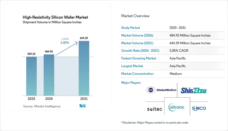
고저항 실리콘 웨이퍼 시장 규모는 2025년 4억 5,933만 평방인치로 평가되었습니다. 2026년에는 4억 8,495만 평방인치로 확대되어 2031년까지 6억 4,439만 평방인치에 이를 것으로 예상되며 2026년부터 2031년에 걸쳐 CAGR 5.85%를 나타낼 전망입니다.
5G 매크로 사이트 및 스몰셀 사이트를 구축하는 통신사들은 RF-SOI 스위치 및 파워앰프의 다년간의 구매 계약을 체결하고 있어, 단말기 출하량 증가세가 둔화되더라도 기본적인 수요는 확보되어 있습니다. 유럽과 중국에서 레벨 2 이상의 운전지원 기능이 의무화되면서 차량 1대당 레이더 탑재량이 증가하고 있으며, 센서가 1개 추가될 때마다 1000 옴센티미터 이상의 저항률을 가진 기판이 필요하게 됩니다. 광집적회로 업체들은 현재 300mm 고저항 플랫폼의 인증을 진행하고 있으며, 웨이퍼의 구성은 더 큰 직경의 웨이퍼로 전환하고 있습니다. 마지막으로, 미국, 유럽, 일본의 정부 인센티브로 인해 국내 생산능력 증설이 가속화되고 있으며, 지정학적 요인으로 인한 공급 충격으로부터 구매자를 보호하고 있습니다.
세계의 고저항 실리콘 웨이퍼 시장 동향과 인사이트
5G 스마트폰에서 RF SOI 채택 확대
현재 모든 5G 단말기에 RF-SOI 프론트엔드 회로가 탑재되어 고저항 실리콘 웨이퍼 시장에 대한 구조적 수요가 확고하게 형성되어 있습니다. HR-SOI의 트랩이 풍부한 층은 2GHz 이상의 주파수에서 기판 결합을 억제하여 전력 증폭기가 외부 필터 없이도 선형성 목표를 달성할 수 있도록 합니다. 스마트폰 1대당 부품 가치는 2020년 1.20달러에서 2024년 2.10달러로 상승했으며, 설계자들은 이미 2027년까지 200mm 웨이퍼의 생산 능력을 확보했습니다. 인도, 동남아시아, 남미에서 6GHz 이하 주파수 대역의 커버리지가 확대됨에 따라, 단말기 출하량 감소에도 불구하고 웨이퍼 수요는 견조하게 유지되고 있습니다.
자동차용 레이더 생산 확대
유럽연합(EU)의 2024년 안전 규정은 신차 한 대당 77-81GHz 대역의 레이더를 여러 개 장착하도록 의무화했으며, 이로 인해 유럽과 북미에서 고저항 웨이퍼의 소비가 증가했습니다. HR-SOI(고저항 SOI) 기반 실리콘 레이더는 77GHz에서 벌크 CMOS보다 위상잡음을 15% 감소시켜 첨단운전자보조기능(ADAS)을 지원합니다. 2025년 중국의 NCAP(국가 자동차 안전도 평가 프로그램)이 강화됨에 따라 국내 브랜드들은 코너 레이더와 후방 레이더 장착을 추진하고 있으며, 향후 10년간 기판 시장의 두 자릿수 성장을 견인할 것으로 예측됩니다.
결함 없는 300mm 고저항 웨이퍼 제조의 복잡성
300mm의 플로트 존 결정 성장에는 엄격한 열 관리가 필요하며, 초기 수율은 200mm 상당 제품에 비해 최대 20% 포인트까지 낮습니다. 300mm HR-SOI 웨이퍼 전체에서 ±2nm 이내의 에피택셜 균일성을 확보하는 것은 여전히 어려운 과제이며, 이는 고객의 인증 프로세스를 지연시키고 있습니다. 신규 생산라인 건설에 8억-12억 달러의 비용이 들기 때문에 신규 진입을 막고, 공정이 성숙할 때까지 공급이 부족하여 현물가격이 계속 상승할 것입니다.
부문 분석
2025년 기준, 200mm 부문은 고저항 실리콘 웨이퍼 시장 점유율의 54.68%를 차지했으며, 이는 2010년대에 건설된 RF-IC 팹의 도입 실적을 반영합니다. Qorvo와 Skyworks와 같은 주요 프론트엔드 업체들은 스위치와 저잡음 증폭기의 다이 사이즈가 여전히 작기 때문에 성숙한 200mm 라인을 계속 가동하고 있습니다. 그러나 300mm 팹은 수율이 안정화되면 다이당 원가절감이 예상되며, 초기 도입 기업들은 2025년 말까지 85%의 수율을 달성하여 200mm 공정과의 격차를 좁혔습니다. 시설당 10억 달러에 육박하는 설비 투자 비용으로 인해 전환이 지연되고 있지만, RF, 베이스밴드, AI 가속기를 하나의 다이에 통합할 수 있다는 점에서 대형 포맷은 경제적으로 매력적입니다.
향후 300mm 부문은 연간 6.74%의 성장률을 보이며 고저항 실리콘 웨이퍼 시장에서 200mm의 우위를 점진적으로 잠식해 나갈 것으로 예측됩니다. 디지털 신호 처리를 통합한 자동차용 레이더 IC는 채널 수가 증가함에 따라 다이 면적이 120mm2를 초과하여 선구적인 제품 중 하나가 될 것입니다. 150mm 기판은 여전히 기존 군사 프로그램에서 사용되고 있지만, 절대 생산량은 감소하는 추세입니다. 수율에 대한 학습이 진행되고, 텍사스, 프라이버그, 구미에서 보조금에 의한 생산능력 확대가 진행됨에 따라, 대량 생산되는 RF 디바이스에서 300mm 웨이퍼의 경제성은 결정적으로 유리하게 작용할 것입니다.
2025년에는 이미징 센서 및 산업용 검출기에서 RF 절연보다 낮은 암전류에 대한 중요성이 부각되면서 폴리싱된 고저항 실리콘이 38.86%의 시장 점유율을 차지했습니다. 에피택셜 웨이퍼는 전력 소자 및 MEMS를 지원하며, 저도핑 에피층은 전압 차단 및 기계적 이점을 제공합니다. 그러나 5G, Wi-Fi 7, 위상배열 레이더가 고도의 선형성을 요구함에 따라 HR-SOI는 연평균 6.48%의 연평균 복합 성장률(CAGR)로 확대될 것으로 예측됩니다. RFeSI-3 플랫폼은 고조파 왜곡을 2dB 감소시켜 26dBm 파워앰프에서 HR-SOI를 필수적인 요소로 만듭니다.
GlobalFoundries, TSMC 및 기타 파운드리 업체들이 300mm 웨이퍼에서 HR-SOI 인증을 진행함에 따라 채택이 가속화되고 있으며, 이로 인해 웨이퍼당 유효 다이 수가 실질적으로 두 배로 증가하여 비용 증가가 줄어들고 있습니다. 따라서 HR-SOI 기판용 고저항 실리콘 웨이퍼 시장 규모는 전체 시장보다 빠르게 확대될 것으로 예측됩니다. 공급 집중은 여전히 양날의 검입니다. 소이텍이 60%의 점유율을 차지하여 품질 안정성은 확보되어 있지만, 생태계가 단일 장애점에 노출될 위험도 있기 때문에 Tier 1 IC 제조업체들은 가능한 한 신에츠화학공업과 SUMCO에서 듀얼 소싱을 하고 있습니다.
"고저항 실리콘 웨이퍼 시장 보고서는 웨이퍼 직경(150mm, 200mm, 300mm), 웨이퍼 유형(연마, 에피택셜, HR-SOI), 디바이스 용도(RF 프론트엔드 디바이스, mm파 및 5G 트랜시버 IC, 자동차용 레이더 IC 등), 최종 사용자(민생전자, 산업, 자동차 등), 지역별로 분류하여 분석하였습니다. 사용자(가전, 산업용, 자동차 등), 그리고 지역별로 분류되어 있습니다. 시장 예측은 수량(평방인치) 기준으로 제공됩니다.
지역별 분석
아시아태평양은 2025년 58.89%의 시장 점유율로 고저항 실리콘 웨이퍼 시장을 독점했으며, 2031년까지 연평균 6.98%의 성장률을 나타낼 것으로 예측됩니다. 일본의 신에츠화학공업과 SUMCO는 공동으로 전 세계 플로트존 생산능력의 절반을 공급하고 있으며, 대만의 팹리스 RF 기업군은 이들 웨이퍼를 파워앰프로 가공하여 전 세계로 수출하고 있습니다. 중국은 플로트존 생산의 현지화를 위해 적극적으로 투자하고 있으며, 수입 의존도를 낮추는 동시에 일본산 동급 제품보다 20-30% 저렴한 웨이퍼를 제공합니다. 한국의 SK실트론은 지리적 분산을 원하는 자동차용 레이더 공급업체에 대응하기 위해 300mm 웨이퍼 양산 체제를 확대되고 있습니다.
북미에서는 CHIPS법에 따라 특수 웨이퍼 공장 설비투자의 최대 40%까지 보조금을 지원받을 수 있기 때문에 과거 추세를 뛰어넘는 속도로 생산능력이 확대되고 있습니다. GlobalWafers는 4억 달러의 연방정부 보조금을 받아 텍사스 주에서 공사를 시작했으며, 2027년 첫 웨이퍼 출하를 계획하고 있습니다. 이 신규 라인에서는 국내 RF-IC 및 자동차 시장용 300mm HR-SOI를 우선적으로 생산하여 리드타임을 단축하고 무역 리스크를 줄일 수 있습니다. 유럽도 비슷한 길을 걷고 있습니다. 3억 유로(3억 2,500만 달러)의 보조금을 지원받은 실트로닉의 프라이베르크 확장을 통해 이 지역은 수입에만 의존하지 않고 자동차 레이더 생태계를 지원할 수 있는 체제를 갖추게 되었습니다.
남미, 중동, 아프리카는 아직 수요 초기 단계에 있지만, 정책적 노력에 따라 수요가 확대될 가능성이 있습니다. 브라질에서는 5G 초기 도입 시 고저항 실리콘을 내장한 RF 프론트엔드를 수입하고 있으며, 아랍에미레이트에서는 특수 웨이퍼 제조 능력을 갖춘 신규 팹 건설을 검토하고 있습니다. 현재 아프리카에서의 보급은 극히 미미하지만, 남아공의 자동차 부문은 기술 격차를 줄이고 있으며, 향후에는 레이더 IC, 나아가 고저항 기판이 필요하게 될 것입니다. 이들 지역은 2031년까지 기여도가 낮은 지역으로 향후 10년간의 다각화 대안이 될 것입니다.
기타 혜택 :
- 엑셀 형식 시장 예측(ME) 시트
- 3개월간 애널리스트 지원
자주 묻는 질문
목차
제1장 서론
제2장 조사 방법
제3장 주요 요약
제4장 시장 구도
제5장 시장 규모와 성장 예측
제6장 경쟁 구도
제7장 시장 기회와 향후 전망
KTHThe high-resistivity silicon wafer market size is expected to increase from 459.33 million square inches in 2025 to 484.95 million square inches in 2026 and reach 644.39 million square inches by 2031, growing at a CAGR of 5.85% over 2026-2031.
Operators rolling out 5G macro and small-cell sites have locked in multi-year purchases of RF-SOI switches and power amplifiers, guaranteeing baseline demand even as handset unit growth slows. Radar content per car is rising because Level 2+ assistance features are becoming mandatory in Europe and China, and each additional sensor requires substrates with resistivity above 1,000 ohm-cm. Photonic integrated-circuit vendors are now qualifying 300 mm high-resistivity platforms, shifting the wafer mix toward larger diameters. Finally, government incentives in the United States, Europe, and Japan are accelerating domestic capacity additions, cushioning buyers against geopolitical supply shocks.
Global High-Resistivity Silicon Wafer Market Trends and Insights
Growing Adoption of RF SOI in 5G Smartphones
Every 5G handset now ships with RF-SOI front-end circuitry, cementing a structural pull on the high-resistivity silicon wafer market. The trap-rich layer in HR-SOI limits substrate coupling above 2 GHz, letting power amplifiers meet linearity targets without external filters. Component value per phone climbed from USD 1.20 in 2020 to USD 2.10 in 2024, and designers have already reserved 200 mm capacity through 2027. As sub-6 GHz coverage broadens across India, South-East Asia, and South America, wafer demand remains resilient despite plateauing handset units.
Expansion of Automotive Radar Production
The European Union's 2024 safety regulation mandates multiple 77-81 GHz radars per new vehicle, elevating high-resistivity wafer consumption in Europe and North America. Silicon-based radar on HR-SOI delivers 15% lower phase noise than bulk CMOS at 77 GHz, supporting advanced driver-assistance functions. As China's NCAP tightens in 2025, domestic brands are adding corner and rear radar, driving double-digit substrate growth through the decade.
Complexities in Producing Defect-Free 300 mm HR Wafers
Float-zone crystal growth at 300 mm demands stringent thermal control, and initial yields trail 200 mm equivalents by up to 20 percentage points. Epitaxial uniformity within +-2 nm across a 300 mm HR-SOI wafer remains challenging, slowing customer qualifications. The USD 800 million-USD 1.2 billion price tag for a greenfield line deters new entrants, keeping supply tight and inflating spot prices until processes mature.
Other drivers and restraints analyzed in the detailed report include:
- Rising Demand for mmWave Silicon for Satellite Communications
- Integration of Adaptive Beamforming in Phased-Array Antennas
- Price Premium over Conventional Silicon Wafers
For complete list of drivers and restraints, kindly check the Table Of Contents.
Segment Analysis
The 200 mm segment held 54.68% of the high-resistivity silicon wafer market share in 2025, reflecting the installed base of RF-IC fabs built during the 2010s. Leading front-end vendors such as Qorvo and Skyworks continue to run mature 200 mm lines because die sizes for switches and low-noise amplifiers remain small. However, 300 mm fabs promise lower cost per die once yields stabilize, and early adopters saw an 85% yield by late 2025, narrowing the gap with 200 mm processes. Capital costs near USD 1 billion per facility slow the migration, yet the convergence of RF, baseband, and AI accelerators on a single die makes the larger format economically compelling.
Looking forward, the 300 mm segment is expected to grow at a 6.74% rate, gradually eroding the dominance of 200 mm in the high-resistivity silicon wafer market. Automotive radar ICs integrating digital signal processing will be among the first movers because rising channel counts drive die area beyond 120 mm2. While 150 mm substrates linger in legacy military programs, their absolute volumes are shrinking. As yield learning improves and subsidy-backed capacity ramps in Texas, Freiberg, and Gumi, 300 mm economics will turn decisively favorable for high-volume RF devices.
Polished high-resistivity silicon captured 38.86% of the market share in 2025, thanks to imaging sensors and industrial detectors that value low dark current over RF isolation. Epitaxial wafers support power devices and MEMS, where a lightly doped epi-layer offers voltage blocking or mechanical benefits. HR-SOI, however, is forecast to rise at a 6.48% CAGR as 5G, Wi-Fi 7, and phased-array radars demand enhanced linearity. The RFeSI-3 platform reduced harmonic distortion by 2 dB, making HR-SOI indispensable for 26 dBm power amplifiers.
Adoption accelerates as GlobalFoundries, TSMC, and other foundries qualify HR-SOI at 300 mm, effectively doubling usable die per wafer and shrinking cost penalties. The high-resistivity silicon wafer market size for HR-SOI substrates is therefore set to expand more quickly than the total market volume. Supply concentration remains a double-edged sword: Soitec's 60% share offers stable quality but exposes the ecosystem to single-point failures, prompting tier-1 IC houses to dual-source from Shin-Etsu and SUMCO where possible.
The High-Resistivity Silicon Wafer Market Report is Segmented by Wafer Diameter (150 Mm, 200 Mm, and 300 Mm), Wafer Type (Polished, Epitaxial, and HR-SOI), Device Application (RF Front-End Devices, Mmwave and 5G Transceiver ICs, Automotive Radar ICs, and More), End-User (Consumer Electronics, Industrial, Automotive, and More ), and Geography. The Market Forecasts are Provided in Terms of Volume (Square Inches).
Geography Analysis
Asia-Pacific dominated the high-resistivity silicon wafer market with 58.89% market share in 2025, and is projected to grow at 6.98% through 2031. Japan's Shin-Etsu and SUMCO jointly supply half the world's float-zone capacity, while Taiwan's fabless RF community converts those substrates into power amplifiers exported globally. China is investing aggressively to localize float-zone production, reducing import dependence and offering wafers 20-30% cheaper than Japanese equivalents. South Korea's SK Siltron is ramping 300 mm qualification to serve automotive radar suppliers seeking geographic diversity.
North America is adding capacity faster than historical trends because the CHIPS Act covers up to 40% of capital expenditures for specialty wafer plants. GlobalWafers broke ground in Texas with USD 400 million in federal grants, and first wafers are slated for 2027. These new lines will prioritize 300 mm HR-SOI for domestic RF-IC and automotive markets, shortening lead times and mitigating trade risks. Europe follows a similar path; Siltronic's Freiberg expansion, backed by EUR 300 million (USD 325 million) in subsidies, positions the region to support its automotive radar ecosystem without relying solely on imports.
South America and the Middle East and Africa remain nascent consumers, but policy initiatives could unlock incremental demand. Brazil's initial 5G rollout is importing RF front-ends that incorporate high-resistivity silicon, while the United Arab Emirates is studying a greenfield fab that would include specialty wafer capability. African uptake is negligible today, yet South Africa's automotive sector is narrowing technology gaps that will eventually require radar ICs and, by extension, HR substrates. Although these regions contribute minimally before 2031, they represent diversification options in the next decade.
- Shin-Etsu Handotai Co., Ltd.
- SUMCO Corporation
- Siltronic AG
- GlobalWafers Co., Ltd.
- Soitec S.A.
- Okmetic Oyj
- Wafer Works Corp.
- SK Siltron Co., Ltd.
- Zhejiang Ferrotec Semiconductor Co., Ltd.
- Addison Engineering, Inc.
- Topsil Semiconductor Materials A/S
- SINO-American Silicon Products Inc.
- Wafer World Inc.
- Virginia Semiconductor, Inc.
- Shanghai Simgui Technology Co., Ltd.
- Nova Electronic Materials, LLC
- Ferrotec Holdings Corporation
- pSemi Corporation
Additional Benefits:
- The market estimate (ME) sheet in Excel format
- 3 months of analyst support
TABLE OF CONTENTS
1 INTRODUCTION
- 1.1 Study Assumptions and Market Definition
- 1.2 Scope of the Study
2 RESEARCH METHODOLOGY
3 EXECUTIVE SUMMARY
4 MARKET LANDSCAPE
- 4.1 Market Overview
- 4.2 Market Drivers
- 4.2.1 Growing Adoption of RF SOI in 5G Smartphones
- 4.2.2 Expansion of Automotive Radar Production
- 4.2.3 Rising Demand for mmWave Silicon for Satellite Communications
- 4.2.4 Integration of Adaptive Beamforming in Phased-Array Antennas
- 4.2.5 Development of Photonic ICs on High-Resistivity Substrates
- 4.2.6 Government Incentives for On-shore Semiconductor Manufacturing
- 4.3 Market Restraints
- 4.3.1 Complexities in Producing Defect-Free 300 mm HR Wafers
- 4.3.2 Price Premium over Conventional Silicon Wafers
- 4.3.3 Supply Constraints of Ultra-High-Purity Float-Zone Silicon
- 4.3.4 Emerging GaN and SiC Substrates for RF and Power Devices
- 4.4 Industry Supply-Chain Analysis
- 4.5 Regulatory Landscape
- 4.6 Technological Outlook
- 4.7 Impact of Macroeconomic Factors on the Market
- 4.8 Porter's Five Forces Analysis
- 4.8.1 Threat of New Entrants
- 4.8.2 Bargaining Power of Suppliers
- 4.8.3 Bargaining Power of Buyers
- 4.8.4 Threat of Substitutes
- 4.8.5 Intensity of Competitive Rivalry
5 MARKET SIZE AND GROWTH FORECASTS (VOLUME)
- 5.1 By Wafer Diameter
- 5.1.1 150 mm
- 5.1.2 200 mm
- 5.1.3 300 mm
- 5.2 By Wafer Type
- 5.2.1 Polished High-Resistivity Silicon
- 5.2.2 Epitaxial High-Resistivity Silicon
- 5.2.3 High-Resistivity Silicon-on-Insulator (HR-SOI)
- 5.3 By Device Application
- 5.3.1 RF Front-End Devices (PA, Switches, LNAs)
- 5.3.2 mmWave and 5G Transceiver ICs
- 5.3.3 Automotive Radar ICs (77-81 GHz)
- 5.3.4 Photodetectors and Imaging Devices
- 5.3.5 MEMS and Advanced Sensor ICs
- 5.4 By End-user
- 5.4.1 Consumer Electronics
- 5.4.2 Industrial
- 5.4.3 Telecommunications
- 5.4.4 Automotive
- 5.4.5 Other End-user Applications
- 5.5 By Geography
- 5.5.1 North America
- 5.5.1.1 United States
- 5.5.1.2 Canada
- 5.5.1.3 Mexico
- 5.5.2 Europe
- 5.5.2.1 Germany
- 5.5.2.2 United Kingdom
- 5.5.2.3 France
- 5.5.2.4 Rest of Europe
- 5.5.3 Asia-Pacific
- 5.5.3.1 China
- 5.5.3.2 Japan
- 5.5.3.3 India
- 5.5.3.4 South Korea
- 5.5.3.5 Rest of Asia-Pacific
- 5.5.4 South America
- 5.5.5 Middle East and Africa
- 5.5.1 North America
6 COMPETITIVE LANDSCAPE
- 6.1 Market Concentration
- 6.2 Strategic Moves
- 6.3 Market Share Analysis
- 6.4 Company Profiles (includes Global level Overview, Market Level Overview, Core Segments, Financials as Available, Strategic Information, Market Rank/Share for Key Companies, Products and Services, and Recent Developments)
- 6.4.1 Shin-Etsu Handotai Co., Ltd.
- 6.4.2 SUMCO Corporation
- 6.4.3 Siltronic AG
- 6.4.4 GlobalWafers Co., Ltd.
- 6.4.5 Soitec S.A.
- 6.4.6 Okmetic Oyj
- 6.4.7 Wafer Works Corp.
- 6.4.8 SK Siltron Co., Ltd.
- 6.4.9 Zhejiang Ferrotec Semiconductor Co., Ltd.
- 6.4.10 Addison Engineering, Inc.
- 6.4.11 Topsil Semiconductor Materials A/S
- 6.4.12 SINO-American Silicon Products Inc.
- 6.4.13 Wafer World Inc.
- 6.4.14 Virginia Semiconductor, Inc.
- 6.4.15 Shanghai Simgui Technology Co., Ltd.
- 6.4.16 Nova Electronic Materials, LLC
- 6.4.17 Ferrotec Holdings Corporation
- 6.4.18 pSemi Corporation
7 MARKET OPPORTUNITIES AND FUTURE OUTLOOK
- 7.1 White-space and Unmet-Need Assessment