
|
시장보고서
상품코드
2044015
5G 반도체 실리콘 웨이퍼 : 시장 점유율 분석, 업계 동향 및 통계, 성장 예측(2026-2031년)5G Semiconductor Silicon Wafer - Market Share Analysis, Industry Trends & Statistics, Growth Forecasts (2026 - 2031) |
||||||
 Mordor Intelligence
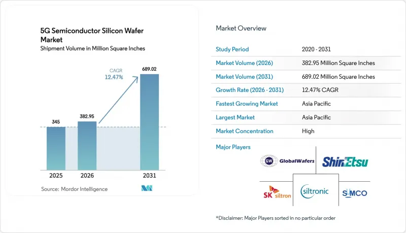
5G 반도체 실리콘 웨이퍼 시장 규모는 2025년 3억 4,500만 평방인치로 평가되었습니다. 2026년에는 3억 8,295만 평방인치로 확대되어 2026년부터 2031년에 걸쳐 CAGR 12.47%를 나타내, 2031년에는 6억 8,902만 평방인치에 이를 것으로 예측됩니다.
스마트폰의 7나노미터 이하로의 전환, 도시 지역 5G 인프라의 집적화, 300mm 웨이퍼로의 지속적인 전환은 5G 반도체 실리콘 웨이퍼 시장의 구조적 성장 동력이 되고 있습니다. 아시아태평양의 휴대폰 제조업체들의 견고한 조달은 파운더리의 장기적인 생산량을 보장하는 한편, 북미 및 유럽 온쇼어링 프로그램은 아시아태평양의 우위를 훼손하지 않고 공급 지역을 다변화하고 있습니다. 기판 공급 부족으로 상위 5개 웨이퍼 업체들은 매년 가격 인상을 추진하고 있으며, 두산의 SK실트론 인수 등 최근 업계 재편은 기존 업체들의 협상력을 더욱 강화시키고 있습니다. 초순수 사용에 대한 환경 규제와 폴리실리콘 가격 변동은 수익률 확대를 억제하고 있지만, 5G 반도체 실리콘 웨이퍼 시장의 성장 궤도를 뒷받침하는 설비 투자 계획을 좌절시키지는 못했습니다.
세계의 5G 반도체 실리콘 웨이퍼 시장 동향과 인사이트
5G 스마트폰으로 인한 모바일 데이터 트래픽 급증
세계 5G 단말기 출하량은 2024년 12억 대에 달했으며, 2026년까지 15억 대에 달할 것으로 예측됩니다. 각 하이엔드 단말기는 웨이퍼 면적을 크게 소비하는 7나노미터 이하의 다이에 의존하고 있습니다. 190억 개의 트랜지스터를 탑재한 애플의 A18 Pro와 같은 플래그십 프로세서는 EUV 패터닝 결함을 피하기 위해 0.3마이크로미터 미만의 실리콘 평탄도를 필요로 합니다. 파운드리 업체들은 300mm 웨이퍼의 생산 능력을 최대 1년 전부터 예약하고 있으며, 이로 인해 기판의 정가는 전년 대비 12%-15% 상승했습니다. 20나노미터 미만의 미세 입자 하나가 전체 최첨단 다이를 망가뜨릴 수 있기 때문에 고객들은 1cm2당 결함 수가 0.01 미만인 에피택셜 품질 웨이퍼로의 전환을 가속화하고 있으며, 5G 반도체 실리콘 웨이퍼 시장에서 프리미엄 계약을 확보하고 있습니다.
5G 통신 인프라의 신속한 구축
중국은 2024년 12월까지 420만 개의 5G 기지국을 설치했고 2025년 말까지 500만 개를 목표로 했며, 디지털 베이스밴드가 7나노미터로 전환되는 동안 RF 프론트엔드에 대한 성숙된 노드 수요를 유지하고 있습니다. 유럽의 통신 사업자들은 7나노미터 ASSP를 통합한 에릭슨의 RAN 컴퓨팅 시스템을 활용하여 스몰셀 구축을 가속화하고 있습니다. 이러한 고밀도화의 물결은 평방 킬로미터당 필요한 사이트 수를 두 배로 늘리고, 180 나노미터에서 7 나노미터에 이르는 혼합 노드 웨이퍼 수요를 증가시키고 있습니다. 따라서 5G 반도체 실리콘 웨이퍼 시장에 공급하는 업체들은 노드 변동 리스크를 헤지하기 위해 200mm와 300mm 생산 공정을 병행하여 계획하고 있습니다.
300mm 웨이퍼 공장의 막대한 설비 투자
300mm 팹의 신규 건설에 100억-200억 달러의 비용이 소요되기 때문에 신규 진입이 드물고, 가격 결정력을 뒷받침하는 과점 구조가 강화되고 있습니다. GlobalWafers의 75억 달러 규모의 텍사스 프로젝트는 미국으로부터 15억 달러의 보조금을 받았지만, 수익화까지 5년의 가동 기간이 필요합니다. SUMCO는 재투자하는 대신 기존 200mm 라인을 폐쇄하기로 결정했습니다. 이는 회수 기간이 길어지면 기존 기업들조차도 소규모 자산에서 철수할 것임을 시사합니다. 그 결과,월5만 웨이퍼 단위의 생산능력을 단계적으로 확대하여 5G 반도체 실리콘 웨이퍼 시장공급탄력성을 제한하고 있습니다.
부문 분석
300mm 카테고리는 2025년 59.32%의 시장 점유율을 차지했으며 CAGR 13.23%의 혜택을 받아 2031년까지 그 우위를 확고히할 것으로 예측됩니다. 300mm 웨이퍼 1장당 다이 수는 200mm 웨이퍼의 약 2.4배이며, 감가상각분을 고려하면 단위당 제조비용은 30%-35% 낮습니다. 애리조나, 평택, 아일랜드의 주요 팹에서는 이 직경만 처리하고 있어 안정적인 기준선 수요가 확보되어 있습니다. 따라서 5G 반도체 실리콘 웨이퍼 시장에서 300mm 기판 시장 규모는 다른 어떤 직경의 기판보다 빠르게 확대될 것입니다.
기존 RF, 파워, MEMS용으로는 여전히 200mm가 필수적이지만, 설비투자 계획에서는 기판위 웨이퍼(COWS) 패키징을 위한 초박형 연마가 가능한 300mm 라인이 압도적으로 중요시되고 있습니다. 50마이크로미터 미만의 휨 없는 박형화를 보장할 수 있는 공급업체는 고부가가치 계약을 따내고, 후발업체는 자동차 및 산업용 바이어를 위한 200마이크로미터 서비스 안정화에 주력하고 있습니다. 이러한 양극화는 광범위한 5G 반도체 실리콘 웨이퍼 시장에서 장기적인 성장을 보장하고 경기변동의 영향을 완화할 수 있습니다.
"5G 반도체 웨이퍼 시장 보고서는 웨이퍼 직경(300mm 및 200mm), 기술 노드(첨단 노드, 주류 노드, 성숙 노드), 최종 용도(스마트폰, 통신 인프라, 고정형 무선 액세스, 산업용 5G), 지역(북미, 유럽, 아시아태평양, 기타)별로 분류되어 있습니다. 로 분류되어 있습니다. 시장 예측은 수량(평방인치) 기준으로 제공됩니다.
지역별 분석
아시아태평양은 2025년 5G 반도체 웨이퍼 시장의 72.61%를 차지했으며 2031년까지 연평균 복합 성장률(CAGR) 13.83%로 확대될 것으로 예측됩니다. 중국의 420만 개의 매크로 기지국과 대만의 파운드리 클러스터가 결합하여 독보적인 수요처를 창출하고 있는 반면, 일본 웨이퍼 공급업체는 전 세계 300mm 웨이퍼 생산량의 절반 이상을 차지하고 있습니다. 지역 정책, 특히 베이징의 현지화 의무와 도쿄의 첨단 포장에 대한 보조금 제도는 생산 능력을 더욱 공고히 하고, 이 지역의 주도적 지위를 강화하고 있습니다.
북미는 텍사스, 애리조나, 뉴욕, 오하이오의 팹에 보조금을 지급하는 미국의 'CHIPS and Science Act(CHIPS and Science Act)'를 통해 전략적으로 존재감을 높이고 있습니다. 2028년까지 이들 공장이 본격 가동되면 연간 약 3,000만-3,500만 평방인치의 웨이퍼를 소비할 것으로 예상되며, 이는 세계 점유율의 약 10%에 해당합니다. 이를 통해 아시아의 생산량 우위를 크게 훼손하지 않으면서도 국방 및 핵심 인프라에 대한 국내 공급을 확보할 수 있게 됩니다. 캐나다와 멕시코는 보완적인 백엔드 및 성숙한 노드에 대한 투자를 가속화하여 5G 반도체 실리콘 웨이퍼 시장을 지원하는 대륙 규모의 생태계를 완성할 것입니다.
유럽의 '칩스법'은 신규 생산능력에 430억 유로(470억 달러)를 투입하고, 마그데부르크와 드레스덴의 생산기지가 본격 가동되면 이 지역의 웨이퍼 수요를 2025년 8%에서 2030년까지 12%-14%까지 끌어올릴 수 있을 것으로 예상했습니다. 남미, 중동 및 아프리카의 총 점유율은 여전히 3% 미만에 불과하지만, 브라질의 자동차 전동화와 아랍에미리트(UAE)의 데이터센터 구축에 힘입어 성장이 예상됩니다. 이러한 소규모 지역이라 할지라도 5G 반도체 실리콘 웨이퍼 시장의 세계 확산 범위를 넓히는 역할을 하고 있습니다.
기타 혜택 :
- 엑셀 형식 시장 예측(ME) 시트
- 3개월간 애널리스트 지원
자주 묻는 질문
목차
제1장 서론
제2장 조사 방법
제3장 주요 요약
제4장 시장 구도
제5장 시장 규모와 성장 예측
제6장 경쟁 구도
제7장 시장 기회와 향후 전망
KTH 26.05.29The 5G semiconductor silicon wafer market size is expected to grow from 345 million square inches in 2025 to 382.95 million square inches in 2026, and is forecast to reach 689.02 million square inches by 2031, at a 12.47% CAGR over 2026-2031. Sub-7-nanometer migration across smartphones, densification of urban 5G infrastructure, and sustained conversion to 300-millimeter substrates remain the structural growth engines for the 5G semiconductor silicon wafer market. Strong procurement from Asia-Pacific handset makers secures long-term foundry output, while North American and European onshoring programs diversify geographic supply without displacing the region's dominance. Tight substrate availability enables the top five wafer makers to push annual price escalators, and recent consolidation, such as Doosan's purchase of SK Siltron, intensifies the negotiating leverage of incumbents. Environmental restrictions on ultra-pure water usage and polysilicon price swings temper margin expansion but have not derailed capex programs that underpin the 5G semiconductor silicon wafer market's growth trajectory.
Global 5G Semiconductor Silicon Wafer Market Trends and Insights
Surging Mobile Data Traffic from 5G Smartphones
Global 5G handset shipments reached 1.2 billion in 2024 and are forecast to hit 1.5 billion by 2026, each premium device relying on sub-7 nanometer dies that consume materially larger wafer area. Flagship processors, such as Apple's A18 Pro with 19 billion transistors, demand silicon flatness below 0.3 micrometers to avoid EUV patterning defects. Foundries pre-book 300 millimeter capacity up to a year ahead, pushing substrate list prices 12%-15% higher year-on-year. Because a single sub-20 nanometer particle can kill an entire advanced die, customers increasingly shift to epitaxial-quality wafers with <0.01 defects per cm2, locking in premium contracts for the 5G semiconductor silicon wafer market.
Rapid Deployment of 5G Telecom Infrastructure
China installed 4.2 million 5G base stations by December 2024 and targets 5 million by end-2025, retaining mature-node demand for RF front-ends while digital baseband moves to 7 nanometers. European operators accelerated small-cell rollouts using Ericsson's RAN Compute systems that integrate 7 nanometer ASSPs. The densification wave multiplies required sites per square kilometer, lifting mixed-node wafer demand spanning 180 nanometers to 7 nanometers. Suppliers serving the 5G semiconductor silicon wafer market, therefore, schedule overlapping 200 millimeter and 300 millimeter production runs to hedge node volatility.
High Capital Expenditure for 300 mm Wafer Fabs
Building a greenfield 300 millimeter plant costs USD 10 billion-USD 20 billion, keeping new entry rare and reinforcing the oligopoly that underpins pricing power. GlobalWafers' USD 7.5 billion Texas project received USD 1.5 billion in U.S. grants, yet still faces a five-year ramp before revenue begins. SUMCO elected to close a legacy 200 millimeter line rather than reinvest, signaling that even incumbents exit sub-scale assets when payback periods lengthen. Resulting capacity staging in 50,000-wafer-per-month increments limits supply elasticity for the 5G semiconductor silicon wafer market.
Other drivers and restraints analyzed in the detailed report include:
- Increasing Demand for Advanced Node Chips in 5G Devices
- Adoption of Silicon Wafer Thinning for 5G mmWave Antenna Integration
- Supply Chain Disruptions of Semiconductor Grade Polysilicon
For complete list of drivers and restraints, kindly check the Table Of Contents.
Segment Analysis
The 300 millimeter category held 59.32% of the market share in 2025 and benefits from a 13.23% CAGR, cementing its primacy through 2031. Each 300-millimeter wafer yields roughly 2.4X the die count of a 200-millimeter wafer, translating to 30%-35% lower unit fabrication cost once depreciation is absorbed. Leading fabs in Arizona, Pyeongtaek, and Ireland process only this diameter, ensuring locked-in baseline demand. The 5G semiconductor silicon wafer market size for 300 millimeter substrates will therefore scale faster than any other diameter set.
Although 200 millimeters remains indispensable for legacy RF, power, and MEMS, capital plans heavily favor 300 millimeter lines capable of ultra-thin grinding for chip-on-wafer-on-substrate packaging. Suppliers able to guarantee warp-free thinning below 50 micrometers capture premium contracts, while second-tier producers focus on stabilizing 200-micrometer service for automotive and industrial buyers. This bifurcation secures long-run growth and cushions cyclicality within the broader 5G semiconductor silicon wafer market.
The 5G Semiconductor Silicon Wafer Market Report is Segmented by Wafer Diameter (300 Mm and 200 Mm), Technology Node (Advanced Node, Mainstream Node, and Mature Node), End Application (Smartphones, Telecom Infrastructure, Fixed Wireless Access, and Industrial 5G), and Geography (North America, Europe, Asia-Pacific, and More). The Market Forecasts are Provided in Terms of Volume (Square Inches).
Geography Analysis
Asia-Pacific controlled 72.61% of the 5G semiconductor silicon wafer market in 2025 and expands at 13.83% CAGR through 2031. China's 4.2 million macro base stations and Taiwan's foundry cluster together generate unrivaled demand pools, while Japanese wafer suppliers command more than half of global 300 millimeter output. Regional policy, notably Beijing's localization mandates and Tokyo's advanced packaging subsidies, further anchors capacity and reinforces the region's leadership position.
North America captures strategic mindshare through the U.S. CHIPS and Science Act, which subsidizes fabs in Texas, Arizona, New York, and Ohio. Once fully online by 2028, these sites will consume roughly 30-35 million square inches annually about 10% global share securing domestic supply for defense and critical infrastructure without materially eroding Asia's volume lead. Canada and Mexico accelerate complimentary back-end and mature-node investments, rounding out a continental ecosystem that supports the 5G semiconductor silicon wafer market.
Europe's Chips Act channels EUR 43 billion (USD 47 billion) into new capacity, lifting regional wafer demand from 8% in 2025 toward an expected 12%-14% by 2030 once sites in Magdeburg and Dresden ramp. South America and the Middle East and Africa jointly remain below 3% share, with growth tied to automotive electrification in Brazil and data-center deployments in the United Arab Emirates. These smaller regions nonetheless widen the global footprint of the 5G semiconductor silicon wafer market.
List of Companies Covered in this Report:
- Shin-Etsu Chemical Co., Ltd.
- SUMCO Corporation
- GlobalWafers Co., Ltd.
- Siltronic AG
- SK Siltron Co., Ltd.
- Wafer Works Corporation
- Gritek Electronics Co., Ltd.
- Addison Engineering, Inc.
- Ferrotec Holdings Corporation
- Okmetic Oyj
- LG Electronics Inc. (Wafer Business)
- Taiwan Semiconductor Manufacturing Company Limited
- Samsung Electronics Co., Ltd.
- GlobalFoundries Inc.
- Semiconductor Manufacturing International Corporation
- United Microelectronics Corporation
- Tower Semiconductor Ltd.
- Vanguard International Semiconductor Corporation
- Powerchip Semiconductor Manufacturing Corporation
- onsemi
Additional Benefits:
- The market estimate (ME) sheet in Excel format
- 3 months of analyst support
TABLE OF CONTENTS
1 INTRODUCTION
- 1.1 Study Assumptions and Market Definition
- 1.2 Scope of the Study
2 RESEARCH METHODOLOGY
3 EXECUTIVE SUMMARY
4 MARKET LANDSCAPE
- 4.1 Market Overview
- 4.2 Market Drivers
- 4.2.1 Surging Mobile Data Traffic from 5G Smartphones
- 4.2.2 Rapid Deployment of 5G Telecom Infrastructure
- 4.2.3 Increasing Demand for Advanced Node Chips in 5G Devices
- 4.2.4 Adoption of Silicon Wafer Thinning for 5G mmWave Antenna Integration
- 4.2.5 Growth of Private 5G Networks in Industrial Automation
- 4.2.6 Government Incentives for Localized Wafer Fabrication in Emerging Economies
- 4.3 Market Restraints
- 4.3.1 High Capital Expenditure for 300 mm Wafer Fabs
- 4.3.2 Supply Chain Disruptions of Semiconductor Grade Polysilicon
- 4.3.3 Yield Challenges at <7nm Nodes for RF Front-End ICs
- 4.3.4 Environmental Regulations Limiting Ultra-Pure Water Usage in Wafer Production
- 4.4 Industry Supply-Chain Analysis
- 4.5 Regulatory Landscape
- 4.6 Technological Outlook
- 4.7 Impact of Macroeconomic Factors on the Market
- 4.8 Porter's Five Forces Analysis
- 4.8.1 Threat of New Entrants
- 4.8.2 Bargaining Power of Suppliers
- 4.8.3 Bargaining Power of Buyers
- 4.8.4 Threat of Substitutes
- 4.8.5 Intensity of Competitive Rivalry
5 MARKET SIZE AND GROWTH FORECASTS (VOLUME)
- 5.1 By Wafer Diameter
- 5.1.1 300 mm
- 5.1.2 200 mm
- 5.2 By Technology Node
- 5.2.1 Advanced Node (Below 7nm)
- 5.2.2 Mainstream Node (10nm-28nm)
- 5.2.3 Mature Node (Above 28nm)
- 5.3 By End Application
- 5.3.1 Smartphones
- 5.3.2 Telecom Infrastructure (Macro / Small Cells)
- 5.3.3 Fixed Wireless Access (FWA)
- 5.3.4 Industrial 5G
- 5.4 By Geography
- 5.4.1 North America
- 5.4.1.1 United States
- 5.4.1.2 Canada
- 5.4.1.3 Mexico
- 5.4.2 Europe
- 5.4.2.1 Germany
- 5.4.2.2 United Kingdom
- 5.4.2.3 France
- 5.4.2.4 Rest of Europe
- 5.4.3 Asia-Pacific
- 5.4.3.1 China
- 5.4.3.2 Japan
- 5.4.3.3 India
- 5.4.3.4 South Korea
- 5.4.3.5 Taiwan
- 5.4.3.6 Rest of Asia-Pacific
- 5.4.4 South America
- 5.4.5 Middle East and Africa
- 5.4.1 North America
6 COMPETITIVE LANDSCAPE
- 6.1 Market Concentration
- 6.2 Strategic Moves
- 6.3 Market Share Analysis
- 6.4 Company Profiles (includes Global level Overview, Market Level Overview, Core Segments, Financials as Available, Strategic Information, Market Rank/Share for Key Companies, Products and Services, and Recent Developments)
- 6.4.1 Shin-Etsu Chemical Co., Ltd.
- 6.4.2 SUMCO Corporation
- 6.4.3 GlobalWafers Co., Ltd.
- 6.4.4 Siltronic AG
- 6.4.5 SK Siltron Co., Ltd.
- 6.4.6 Wafer Works Corporation
- 6.4.7 Gritek Electronics Co., Ltd.
- 6.4.8 Addison Engineering, Inc.
- 6.4.9 Ferrotec Holdings Corporation
- 6.4.10 Okmetic Oyj
- 6.4.11 LG Electronics Inc. (Wafer Business)
- 6.4.12 Taiwan Semiconductor Manufacturing Company Limited
- 6.4.13 Samsung Electronics Co., Ltd.
- 6.4.14 GlobalFoundries Inc.
- 6.4.15 Semiconductor Manufacturing International Corporation
- 6.4.16 United Microelectronics Corporation
- 6.4.17 Tower Semiconductor Ltd.
- 6.4.18 Vanguard International Semiconductor Corporation
- 6.4.19 Powerchip Semiconductor Manufacturing Corporation
- 6.4.20 onsemi
7 MARKET OPPORTUNITIES AND FUTURE OUTLOOK
- 7.1 White-Space and Unmet-Need Assessment