
|
시장보고서
상품코드
2043995
유럽의 반도체 실리콘 웨이퍼 : 시장 점유율 분석, 산업 동향 및 통계 데이터, 성장 예측(2026-2031년)Europe Semiconductor Silicon Wafer - Market Share Analysis, Industry Trends & Statistics, Growth Forecasts (2026 - 2031) |
||||||
 Mordor Intelligence
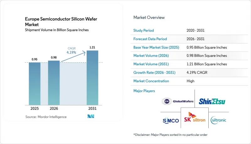
유럽의 반도체 실리콘 웨이퍼 시장 규모(출하량 기반)는 2025년 9억 5,000만 평방인치로 평가되었습니다. 2026년 9억 8,000만 평방인치로부터, 2031년까지 12억 1,000만 평방인치로 확대되며 2026년부터 2031년까지 연평균 복합 성장률(CAGR)은 4.19%를 나타낼 전망입니다.
EU 칩법에 따른 인센티브에 힘입은 파운드리 확장이 지역 공급 구조를 바꾸고 있지만, 범용 기판 시장에서는 여전히 아시아가 지배적이며, 고부가가치 틈새 시장에 집중하는 유럽 공급업체가 진입할 수 있는 여지가 남아있습니다. 자동차의 전동화와 엣지 AI의 도입으로 300mm 프라임 폴리싱 웨이퍼와 실리콘 온 인슐레이터(SOI) 웨이퍼로 수요가 이동하고 있습니다. 파워 디바이스의 200mm 실리콘 카바이드 포맷으로의 전환은 300mm의 성장을 저해하지 않으면서도 공급업체가 공급할 수 있는 공급량을 확대하는 병행 수요의 흐름을 유지하고 있습니다. 경쟁 환경은 자본력이 있는 기존 기업에게 유리하지만, 엔지니어링 기판을 잘 아는 전문 기업들은 5G, 6G 및 양자 컴퓨팅 로드맵에 필수적인 설계 주문을 수주하고 있습니다.
유럽의 반도체 실리콘 웨이퍼 시장 동향과 인사이트
유럽 파운드리의 300mm 웨이퍼 생산 능력 확대
신규 300mm 그린필드 공장이 유럽의 반도체 실리콘 웨이퍼 시장의 비용 곡선을 재구성하고 있습니다. GlobalWafers는 2025년 10월 이탈리아 최초의 300mm 제조 공장을 가동했습니다. 연간 명목 생산능력은 100만장이며, 이 중 60% 이상이 ST마이크로일렉트로닉스 및 인피니언과의 장기 계약으로 확보되어 있습니다. 드레스덴에 설립된 합작법인 'European Semiconductor Manufacturing Company'는 2027년 하반기 파일럿 생산을 시작하면 매월 4만장의 웨이퍼를 추가 공급하여 자동차 노드를 위한 지역 내 기판 수요를 지원하게 됩니다. 2024년 완공되는 실트로닉의 싱가포르 공장 증설에서도 생산능력 배분 제한에 직면한 유럽 바이어를 위해 300mm 웨이퍼 생산량의 일부가 할당될 예정입니다. 이러한 프로젝트가 결합되어 폴리실리콘 가격의 지역적 협상력을 높이고, 자동차 및 산업용에서 중요한 생산량의 물류 루프를 단축할 수 있습니다.
EV 및 재생에너지 그리드에서 전력 전자제품에 대한 수요 증가
전기화 목표에 따라 웨이퍼의 구성은 실리콘과 실리콘 카바이드 모두에서 제조되는 고전압 장치로 전환되고 있습니다. 인피니언은 2025년 1분기 빌라흐에서 200mm SiC 공정 생산을 시작하여 1,200V 이상의 전압을 지원해야 하는 트랙션 인버터를 구현할 수 있게 되었습니다. ST마이크로일렉트로닉스는 4분기에 카타니아에서 비슷한 움직임을 보였으며, 온세미컨덕터는 체코의 엔드투엔드 SiC 생산 능력에 최대 20억 달러를 투자하기로 결정했습니다. EU가 지원하는 'Transform' 및 관련 프로그램은 아시아 잉곳 공급업체에 대한 의존도를 낮추는 유럽 SiC 가치사슬을 구축하고 있습니다. 또한, 견고한 파워 모듈을 채용한 그리드 규모의 태양광용 인버터와 풍력 터빈에서도 수요가 발생하고 있으며, 이로 인해 기판 채용이 더욱 확대되고 있습니다.
유럽 내 폴리실리콘 원료 공급 부족으로 인한 공급 부족
Wacker Chemie의 2025년 7월 에칭 라인 증설로 이 지역의 반도체용 폴리실리콘 생산량이 50% 이상 증가했지만, 유럽은 여전히 원료의 70% 이상을 아시아에서 수입하고 있습니다. 외부 공급원에 대한 과도한 의존은 웨이퍼 제조업체를 지정학적 충격과 가격 급등의 위험에 노출시키고 있습니다. 'Transform' 프로그램에 따라 실리콘 카바이드의 통합 공급망을 구축하려는 노력은 업스트림 공정의 다각화를 제약하는 자본 및 환경 인허가 측면의 장벽이 얼마나 큰지 보여줍니다. 추가 정제 설비가 가동되거나 구속력 있는 장기 인수 계약이 체결되기 전까지는 원자재 부족으로 인해 유럽 웨이퍼 출하량 증가가 억제될 것으로 보입니다.
부문 분석
2025년에는 300mm 노드가 출하량의 73.61%를 차지하여 유럽 팹 브로드맵을 지배하는 로직 및 메모리 공정의 주력 포맷으로 확고히 자리매김했습니다. GlobalWafers의 노바라 공장 가동과 향후 예정된 ESMC 드레스덴 공장의 생산 확대로 연간 300mm 생산 능력에 총 150만장 이상의 웨이퍼가 추가되어 유럽의 반도체 실리콘 웨이퍼 시장은 프라임 폴리싱 기판용 실리콘 웨이퍼 시장이 더욱 확대될 것으로 예측됩니다. 다이당 비용 우위, EUV 리소그래피와의 호환성, 자동차 인증 프로세스 흐름과의 긴밀한 협력으로 300mm의 가동률은 높은 수준을 유지하고 있습니다.
한편, 카바이드(SiC) 파워 디바이스 및 자동차 전동화에 최적화된 아날로그 제품에 힘입어 200mm 웨이퍼에 대한 수요도 꾸준히 이어지고 있습니다. 인피니언(Infineon)의 Villach 공장과 ST마이크로일렉트로닉스(STMicroelectronics)의 Catania 공장의 공정 전환은 결정 성장의 현실과 결함 허용 오차 측면에서 SiC 웨이퍼에 여전히 200mm가 적합하다는 것을 보여줍니다. 여전히 200mm가 적합하다는 것을 보여줍니다. 그 결과, 유럽의 반도체 실리콘 웨이퍼 시장은 300mm가 생산량을 주도하고 200mm가 수익률 안정성을 확보하는 이원화된 구조를 유지하고 있으며, 150mm 이하 라인은 Okmetic의 센서용 제품이 공급하는 MEMS 및 광전자제품의 틈새 시장에 집중하고 있습니다. 시장에 집중하고 있습니다.
로직용 웨이퍼는 2025년 생산량의 32.74%를 차지했으며, 28nm-65nm 노드에 의존하는 엣지 AI 가속기 및 자동차 마이크로컨트롤러의 수혜를 받을 것으로 예측됩니다. 유럽 팹에서는 이러한 프로세스를 대규모로 도입하고 있습니다. TSMC, Bosch, Infineon, NXP의 드레스덴 합작회사는 바로 이러한 미세구조에 초점을 맞추고 있으며, 이로 인해 예측 기간 동안 유럽의 반도체 실리콘 웨이퍼 시장에서 로직용 웨이퍼의 점유율이 확대될 것으로 예측됩니다.
메모리는 유럽 내 범용 D램 생산량이 제한적이기 때문에 점유율은 작지만, FD-SOI 프로젝트와 관련된 임베디드 비휘발성 메모리가 틈새 시장 성장을 견인하고 있습니다. 아날로그 및 혼합 신호 디바이스는 산업 자동화 및 센서 인터페이스 수요에 힘입어 성장하고 있으며, 고전압 구동용 실리콘 카바이드 디스크리트는 유럽의 반도체 실리콘 웨이퍼 시장에서 가장 빠르게 성장하고 있는 분야로 파워 디바이스 제조업체들의 에피택셜 웨이퍼의 주문 러시를 주도하고 있습니다.
'유럽의 반도체 실리콘 웨이퍼 시장 보고서'는 웨이퍼 직경별(150mm 이하, 200mm, 300mm), 반도체 소자 유형별(로직, 메모리, 아날로그, 디스크리트, 옵토일렉트로닉스, 센서, 마이크로), 웨이퍼 유형별(프라임 연마, 에피택셜, SOI, 특수 실리콘), 최종 사용자별(통신, 기타), 국가별로 분류하여 분석하였습니다. 에피택셜, SOI, 특수 실리콘), 최종 사용자별(통신, 기타), 국가별로 분류되어 있습니다. 시장 예측은 출하량(평방인치) 기준으로 제공됩니다.
기타 혜택 :
- 엑셀 형식 시장 예측(ME) 시트
- 3개월간 애널리스트 지원
자주 묻는 질문
목차
제1장 서론
제2장 분석 방법
제3장 주요 요약
제4장 시장 구도
제5장 시장 규모 및 성장률 예측(해당 지역에의 출하량)
제6장 경쟁 구도
제7장 시장 기회와 향후 전망
KTHThe Europe semiconductor silicon wafer market size in terms of shipment volume is projected to expand from 0.95 Billion Square Inches in 2025 and 0.98 Billion Square Inches in 2026 to 1.21 Billion Square Inches by 2031, registering a CAGR of 4.19% between 2026 to 2031.
Foundry expansions backed by EU Chips Act incentives are reshaping regional supply, yet Asia continues to dominate commodity substrates, leaving room for European suppliers focused on higher-value-add niches. Automotive electrification and edge-AI adoption are tilting demand toward 300-mm prime-polished and silicon-on-insulator wafers. Power-device migration to 200 mm silicon carbide formats is sustaining a parallel-diameter stream that widens the supplier's addressable volume without cannibalizing 300 mm growth. Competitive dynamics favor incumbents with capital depth, but specialty players that master engineered substrates are capturing design wins vital to 5G, 6G, and quantum computing roadmaps.
Europe Semiconductor Silicon Wafer Market Trends and Insights
Proliferation of 300 mm Wafer Capacity in European Foundries
New 300 mm greenfield plants are reshaping cost curves for the Europe semiconductor silicon wafer market. GlobalWafers brought Italy's first 300 mm site online in October 2025, with a nameplate output of 1 million wafers per year, of which more than 60% is secured under long-term contracts with STMicroelectronics and Infineon. The European Semiconductor Manufacturing Company joint venture in Dresden will draw an extra 40,000 wafers each month when pilot runs start in late 2027, anchoring regional substrate pull for automotive nodes. Siltronic's Singapore ramp, completed in 2024, also allocates part of its 300 mm output to European buyers facing capacity rationing. Together, these projects lift regional bargaining power on polysilicon pricing and shorten logistics loops for critical automotive and industrial volumes.
Growing Demand for Power Electronics in EV and Renewable Grid
Electrification targets are steering wafer mix toward high-voltage devices fabricated on both silicon and silicon carbide. Infineon began 200 mm SiC processing in Villach during the first quarter of 2025, enabling traction inverters that must handle voltages above 1,200 V. STMicroelectronics mirrored that move at Catania in the fourth quarter, and onsemi committed up to USD 2 billion for end-to-end SiC capacity in the Czech Republic. EU-backed Transform and related programs are knitting together a European SiC value chain that reduces reliance on Asian ingot suppliers. Demand also comes from grid-scale solar inverters and wind turbines that use ruggedized power modules, thereby driving broader substrate uptake.
Limited Polysilicon Feedstock Supply within Europe
Wacker Chemie's July 2025 etching-line expansion lifted regional semiconductor-grade polysilicon output by more than 50% but Europe still imports over 70% of feedstock from Asia. Heavy reliance on external sources exposes wafer makers to geopolitical shocks and price spikes. Building an integrated silicon carbide supply under the Transform program shows the scale of capital and environmental permitting hurdles that constrain upstream diversification. Until additional purification capacity comes online or binding long-term offtake deals are signed, feedstock tightness will cap upside for European wafer shipments.
Other drivers and restraints analyzed in the detailed report include:
- EU Chips Act Incentives for Domestic Semiconductor Manufacturing
- Adoption of Silicon-On-Insulator Wafers for RF and 5G Front-End Modules
- High Capital Intensity and Long ROI Deterring New Entrants
For complete list of drivers and restraints, kindly check the Table Of Contents.
Segment Analysis
The 300 mm node delivered 73.61% of shipments in 2025, confirming its position as the workhorse format for logic and memory processes that dominate European fab roadmaps. GlobalWafers' Novara launch and the forthcoming ESMC Dresden ramp collectively add more than 1.5 million wafers to the annual 300 mm capacity, deepening the Europe semiconductor silicon wafer market for prime-polished substrates. Cost-per-die advantages, compatibility with EUV lithography, and tight coupling to automotive-qualified process flows keep 300 mm utilisation high.
Parallel demand for 200 mm persists, propelled by silicon carbide power devices and analog products tailored to automotive electrification. Infineon's Villach and STMicroelectronics' Catania conversions prove that crystal-growth realities and defect budgets still favor 200 mm for SiC wafers. Consequently, the Europe semiconductor silicon wafer market retains a dual-diameter structure where 300 mm drives volume and 200 mm secures margin resilience, while up to 150 mm lines remain focused on MEMS and optoelectronic niches served by Okmetic's sensor-grade output.
Logic wafers represented 32.74% of 2025 volume, benefiting from edge-AI accelerators and automotive microcontrollers that rely on 28 nm-65 nm nodes, processes that European fabs are adding at scale. The Dresden joint venture between TSMC, Bosch, Infineon, and NXP focuses on precisely those geometries, which should widen the Europe semiconductor silicon wafer market size allocated to logic over the forecast horizon.
Memory holds a smaller slice due to Europe's limited commodity DRAM output, yet embedded non-volatile memory tied to FD-SOI projects keeps niche growth alive. Analog and mixed-signal devices ride industrial automation and sensor interface demand, while silicon carbide discretes for high-voltage drives are the fastest climber in the Europe semiconductor silicon wafer market, spurring a wave of epitaxial wafer orders from power-device manufacturers.
The Europe Semiconductor Silicon Wafer Market Report is Segmented by Wafer Diameter (Up To 150 Mm, 200 Mm, 300 Mm), Semiconductor Device Type (Logic, Memory, Analog, Discrete, Optoelectronics, Sensors, Micro), Wafer Type (Prime Polished, Epitaxial, Silicon-On-Insulator, Specialty Silicon), End-User (Telecommunications, and More), and Country. The Market Forecasts are Provided in Terms of Shipments by Volume (Square Inches).
List of Companies Covered in this Report:
- Shin-Etsu Chemical Co., Ltd.
- SUMCO Corporation
- GlobalWafers Co., Ltd.
- Siltronic AG
- SK siltron Co., Ltd.
- SOITEC S.A.
- Okmetic Oy
- Wafer Works Corporation
- LG Siltron
- Shanghai Simgui Technology Co., Ltd.
- Topsil Semiconductor Materials A/S
- MEMC Electronic Materials, Inc. (GlobalFoundries)
- LOGOS Wafer Manufacturing
- Air Liquide Electronics
- NSIG Group
- Advanced Silicon S.A.
- Sumitomo Mitsubishi Silicon Corporation (SMS)
Additional Benefits:
- The market estimate (ME) sheet in Excel format
- 3 months of analyst support
TABLE OF CONTENTS
1 INTRODUCTION
- 1.1 Study Assumptions and Market Definition
- 1.2 Scope of the Study
2 RESEARCH METHODOLOGY
3 EXECUTIVE SUMMARY
4 MARKET LANDSCAPE
- 4.1 Market Overview
- 4.2 Industry Value-Chain Analysis
- 4.3 Market Drivers
- 4.3.1 Proliferation of 300 mm Wafer Capacity in European Foundries
- 4.3.2 Growing Demand for Power Electronics in EV and Renewable Grid
- 4.3.3 EU Chips Act Incentives for Domestic Semiconductor Manufacturing
- 4.3.4 Adoption of Silicon-on-Insulator Wafers for RF and 5G Front-End Modules
- 4.3.5 Edge AI Adoption Driving 200 mm Logic and Analog Node Revivals
- 4.3.6 Emerging High-Resistivity Wafers for Quantum Computing R&D
- 4.4 Market Restraints
- 4.4.1 Limited Polysilicon Feedstock Supply within Europe
- 4.4.2 High Capital Intensity and Long ROI Deterring New Entrants
- 4.4.3 Geopolitical Dependency on Asia for Wafer Processing Equipment
- 4.4.4 Environmental Regulations Increasing Cost of Ultrapure Water Usage
- 4.5 Regulatory Landscape
- 4.6 Technological Outlook
- 4.7 Impact of Macroeconomic Factors
- 4.8 Porter's Five Forces Analysis
- 4.8.1 Bargaining Power of Suppliers
- 4.8.2 Bargaining Power of Buyers
- 4.8.3 Threat of New Entrants
- 4.8.4 Threat of Substitutes
- 4.8.5 Intensity of Competitive Rivalry
5 MARKET SIZE AND GROWTH FORECASTS (SHIPMENT IN AREA)
- 5.1 By Wafer Diameter
- 5.1.1 Up to 150 mm
- 5.1.2 200 mm
- 5.1.3 300 mm
- 5.2 By Semiconductor Device Type
- 5.2.1 Logic
- 5.2.2 Memory
- 5.2.3 Analog
- 5.2.4 Discrete
- 5.2.5 Optoelectronics
- 5.2.6 Sensors
- 5.2.7 Micro (MCU, MPU, DSP)
- 5.3 By Wafer Type
- 5.3.1 Prime Polished
- 5.3.2 Epitaxial
- 5.3.3 Silicon-on-Insulator (SOI)
- 5.3.4 Specialty Silicon (High-Resistivity, Power, Sensor-Grade)
- 5.4 By End-User
- 5.4.1 Consumer Electronics
- 5.4.1.1 Mobile and Smartphones
- 5.4.1.2 PCs and Servers
- 5.4.2 Industrial
- 5.4.3 Telecommunications
- 5.4.4 Automotive
- 5.4.5 Other End-User Applications
- 5.4.1 Consumer Electronics
- 5.5 By Country
- 5.5.1 Germany
- 5.5.2 France
- 5.5.3 United Kingdom
- 5.5.4 Italy
- 5.5.5 Spain
- 5.5.6 Russia
- 5.5.7 Rest of Europe
6 COMPETITIVE LANDSCAPE
- 6.1 Market Concentration
- 6.2 Strategic Moves
- 6.3 Market Share Analysis
- 6.4 Company Profiles (includes Global Level Overview, Market Level Overview, Core Segments, Financials as available, Strategic Information, Market Rank/Share, Products and Services, Recent Developments)
- 6.4.1 Shin-Etsu Chemical Co., Ltd.
- 6.4.2 SUMCO Corporation
- 6.4.3 GlobalWafers Co., Ltd.
- 6.4.4 Siltronic AG
- 6.4.5 SK siltron Co., Ltd.
- 6.4.6 SOITEC S.A.
- 6.4.7 Okmetic Oy
- 6.4.8 Wafer Works Corporation
- 6.4.9 LG Siltron
- 6.4.10 Shanghai Simgui Technology Co., Ltd.
- 6.4.11 Topsil Semiconductor Materials A/S
- 6.4.12 MEMC Electronic Materials, Inc. (GlobalFoundries)
- 6.4.13 LOGOS Wafer Manufacturing
- 6.4.14 Air Liquide Electronics
- 6.4.15 NSIG Group
- 6.4.16 Advanced Silicon S.A.
- 6.4.17 Sumitomo Mitsubishi Silicon Corporation (SMS)
7 MARKET OPPORTUNITIES AND FUTURE OUTLOOK
- 7.1 White-Space and Unmet-Need Assessment