
|
시장보고서
상품코드
2044003
아시아태평양의 반도체 실리콘 웨이퍼 : 시장 점유율 분석, 업계 동향 및 통계, 성장 예측(2026-2031년)Asia-Pacific Semiconductor Silicon Wafer - Market Share Analysis, Industry Trends & Statistics, Growth Forecasts (2026 - 2031) |
||||||
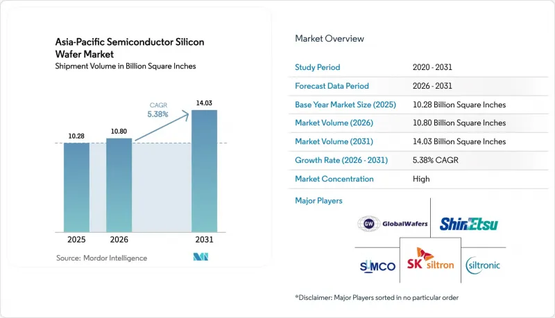
아시아태평양의 반도체 실리콘 웨이퍼 시장 규모(출하량 기반)는 2025년에 102억 8,000만 평방인치로 평가되었습니다. 2026년 108억 평방인치에서 2031년까지 140억 3,000만 평방인치에 이를 것으로 예상되며, 예측 기간(2026-2031년) 중 CAGR 5.38%를 나타낼 것으로 추측되고 있습니다.

중국, 인도, 일본, 일본, 한국의 '자국산 칩' 프로그램 확대가 신규 팹 건설을 주도하고 있으며, 하이퍼스케일 데이터센터와 5G 디바이스로 인해 300mm 프라임 연마 웨이퍼에 대한 수요는 여전히 높은 수준을 유지하고 있습니다. 용인, 평택, 타이난, 구자라트, 홋카이도에 계획된 메가 클러스터는 이미 다년간의 웨이퍼 공급을 확보하여 조달 주기를 단축하고 시장 공급량을 압박하고 있습니다. 동시에, 고주파 프런트엔드 모듈의 SOI(절연막 상 실리콘)로의 전환과 전력 소자의 실리콘 카바이드(SiC) 및 질화갈륨(GaN)으로의 전환은 제품 구성을 변화시키고 있으며, 이로 인해 성숙한 200mm 생산 능력을 아날로그 및 개별 반도체용으로 활용할 수 있게 되었습니다. 에너지 가격 상승으로 인한 가격 압박은 여전히 역풍으로 작용하고 있지만, 수직계열화 및 재생에너지 관련 계약이 주요 제조업체의 부담을 덜어주고 있습니다.
아시아태평양의 반도체 실리콘 웨이퍼 시장 동향과 인사이트
5G 스마트폰 보급률 급증으로 300mm 웨이퍼 수요 급증
5G 단말기의 출하량이 급증함에 따라 프론트엔드 모듈과 애플리케이션 프로세서가 5nm 이하 리소그래피에 대응하는 300mm 기판으로 전환되고 있습니다. 2025년 중국 본토의 조립업체들이 2억 8,000만 대 이상의 5G 스마트폰을 출하했으며, 인도에서는 같은 해 말 기준 5G 가입자 수가 1억 8,000만 명에 달했습니다. 따라서 타이난, 화청, 상하이 파운드리에서는 4nm와 3nm 노드의 가동률이 거의 풀가동 상태입니다. mm파 설계에서는 초저손실 기판이 필수적이기 때문에 고주파용 SOI(절연막상 실리콘)의 채용이 가속화되고 있습니다. 고급 스마트폰의 업그레이드 주기가 길어지면서 역설적으로 대당 실리콘 사용량이 증가하여 판매량이 정체된 상황에서도 웨이퍼 수요를 안정화시키고 있습니다.
국내 반도체 제조에 대한 정부 보조금
현재 이 지역 전체의 설비투자 계획은 재정적 인센티브에 의해 주도되고 있습니다. 일본 내각은 홋카이도의 2nm 파운드리를 위해 2조엔(135억 달러)을 책정했고, 인도의 '반도체 미션'은 인센티브 총액을 150억 달러로 늘렸습니다. 한국은 세액공제를 설비투자금액의 25%로 인상하여 용인에 120조원(910억 달러) 규모의 추가 투자를 촉진했습니다. 중국의 3차 국가IC펀드는 3,440억 위안(470억 달러)을 투입하여 성숙한 노드 확장에 투입했습니다. 이러한 보조금은 장기 계약에 의한 대규모 웨이퍼 주문을 확정하는 것으로, 결과적으로 신규 생산능력이 추가되더라도 현물시장공급량이 줄어들어 가격이 상승할 수 있습니다.
초순수 폴리실리콘 원료의 만성적인 부족 현상
신강의 폴리실리콘 생산량은 2025년 말 에너지 배급령에 따라 18% 감소하고, 현물 가격은 1kg당 30달러를 넘어섰으며, 자체 조달 원료가 없는 웨이퍼 제조업체의 원료 비용은 두 자릿수 증가를 기록했습니다. 토쿠야마와 OCI는 유동층 방식으로 신규 생산능력을 2만 5,000톤 증설하고 있지만, 상업 생산은 2027년 이후부터 시작됩니다. Shin-Etsu Chemical, SUMCO와 같은 대기업은 업스트림 공정에 통합을 통해 수익률을 지키고 있지만, 중소 경쟁사들은 8-12주 정도의 리드타임을 연장해야 하는 부담을 안고 있습니다.
부문 분석
2025년 총 출하량 중 1,300mm급이 71.85%를 차지했습니다. 이는 로직과 고대역폭 메모리의 미세화가 주도한 것입니다. 아시아태평양의 반도체 실리콘 웨이퍼 시장에서 300mm 웨이퍼 시장 규모는 2nm 공정의 게이트 올 어라운드(GaAA) 트랜지스터가 다이 면적을 확대하여 칩당 웨이퍼 수요를 증가시킴에 따라 전체 시장 기준선보다 빠르게 성장할 것으로 예측됩니다. 이 지역에는 이미 42개 팹에 설비가 도입되어 있으며, 신에츠케미칼의 시라카와 공장만 해도 2025년까지 에피택셜 생산량을월80만장까지 끌어올릴 계획입니다.
성숙한 200mm 라인은 실리콘 카바이드로의 전환으로 확보된 생산 능력에 힘입어 아날로그 전원 공급 장치 및 센서 용도를 위해 계속 가동되고 있습니다. 150mm 이하 웨이퍼는 갈륨비소 및 인듐인화물 소자를 위한 5% 이하의 틈새 시장에 머물러 있습니다. 총소유비용(TCO)의 문제로 인해 450mm 파일럿 프로젝트는 어려움을 겪고 있습니다. 결함 밀도가 여전히 손익분기점의 3배에 달하기 때문입니다. 이 근본적인 문제는 450mm 기술이 상업적 타당성을 확보하기 전에 해결해야 할 심각한 기술적, 경제적 장벽을 강조하고 있습니다. 결과적으로, 이러한 지연으로 인해 반도체 제조 산업을 지배하고 있는 기존 300mm 공급망으로의 전환은 계속 미뤄질 것으로 보입니다.
2025년 출하량에서 로직 디바이스가 차지하는 비중은 33.59%로 AI, 5G 베이스밴드, 커스텀 액셀러레이터가 견인했습니다. 아시아태평양의 반도체 실리콘 웨이퍼 시장에서 로직의 점유율은 기록적인 레티클 수로 인해 칩당 웨이퍼 소비량이 증가하고 있으며, 이기종 통합은 기판 수요를 더욱 증가시키고 있습니다. 메모리는 약 30%로 그 뒤를 잇고 있으며, 고 대역폭 메모리의 적층화에 따라 더 두꺼운 연삭 공정과 더 얇은 완성 웨이퍼가 요구되고 있습니다.
아날로그와 디스크리트를 합치면 새로 출시된 200mm 공급의 대부분을 흡수하여 자동차 파워트레인 및 산업 자동화에 기여하고 있습니다. LiDAR 및 비행시간(ToF) 기술이 확산됨에 따라 센서, MEMS, 광전자(각각 한 자릿수 후반의 점유율을 차지)의 총 웨이퍼 수요는 지속적으로 증가하고 있습니다. 이들 부품은 자동차, 가전, 산업 부문을 포함한 다양한 용도에서 중요한 역할을 수행하며 꾸준한 성장을 견인하고 있습니다. 이러한 다각화 전략은 공급업체가 스마트폰 판매의 주기적 변동성을 극복하고 보다 안정적인 수익원을 확보하는 데 도움이 되고 있습니다.
"아시아태평양의 반도체 실리콘 웨이퍼 시장 보고서"는 웨이퍼 직경(150mm 이하, 200mm, 300mm), 반도체 소자 유형(로직, 메모리, 아날로그, 디스크리트, 기타), 웨이퍼 유형(프라임 폴리싱, 에피택셜, 실리콘 온 인슐레이터(SOI), 특수 실리콘), 최종 사용자(PC 및 서버, 산업, 자동차, 기타), 지역별로 구분하여 분석하였습니다. SOI), 특수 실리콘), 최종 사용자(PC 및 서버, 산업용, 자동차용, 기타), 지역별로 분류되어 있습니다. 시장 예측은 출하량(평방인치)으로 제공됩니다.
기타 혜택
- 엑셀 형태 시장 예측(ME) 시트
- 3개월간 애널리스트 지원
자주 묻는 질문
목차
제1장 서론
제2장 조사 방법
제3장 주요 요약
제4장 시장 구도
제5장 시장 규모와 성장 예측
제6장 경쟁 구도
제7장 시장 기회와 향후 전망
KTH 26.05.29The Asia-Pacific Semiconductor Silicon Wafer Market size in terms of shipment volume was valued at 10.28 Billion Square Inches in 2025 and is estimated to grow from 10.80 Billion Square Inches in 2026 to reach 14.03 Billion Square Inches by 2031, at a CAGR of 5.38% during the forecast period (2026-2031).
Rising sovereign-chip programs across China, India, Japan, and South Korea are driving new fab construction, while hyperscale data centers and 5G devices keep demand for 300 mm prime-polished substrates elevated. Planned mega-clusters in Yongin, Pyeongtaek, Tainan, Gujarat, and Hokkaido have already secured multi-year wafer supply, shortening procurement cycles and tightening the merchant pool. Simultaneously, the shift toward silicon-on-insulator for radio-frequency front-end modules and the migration of power devices to silicon-carbide and gallium-nitride are reshaping the mix, freeing mature 200 mm capacity for analog and discretes. Price pressure from energy inflation remains a headwind, yet vertical integration and renewable-energy contracts are cushioning leading producers.
Asia-Pacific Semiconductor Silicon Wafer Market Trends and Insights
Soaring 5G Smartphone Penetration Boosting 300 mm Wafer Demand
A steep rise in 5G handset shipments is shifting front-end modules and application processors onto 300 mm substrates that support sub-5 nm lithography. Mainland assemblers shipped more than 280 million 5G smartphones in 2025, and India ended the same year with 180 million 5G subscribers. Foundries in Tainan, Hwaseong, and Shanghai are therefore operating at near full utilization for 4 nm and 3 nm nodes. Radio-frequency silicon-on-insulator uptake has accelerated as millimeter-wave designs mandate ultra-low loss substrates. Longer upgrade cycles for premium phones paradoxically lift total silicon content per unit, stabilizing wafer pull even when unit sales plateau.
Government Subsidies for Domestic Semiconductor Manufacturing
Fiscal incentives now dominate capital-expenditure roadmaps across the region. The Japanese cabinet earmarked JPY 2 trillion (USD 13.5 billion) for a 2 nm foundry in Hokkaido, and India's Semiconductor Mission raised its incentive pool to USD 15 billion. South Korea raised tax credits to 25% of cap-ex, encouraging an additional KRW 120 trillion (USD 91 billion) commitment in Yongin. China's third National IC Fund injected CNY 344 billion (USD 47 billion) into mature-node expansions. These subsidies lock in large wafer call-offs under long-term contracts, thereby shrinking spot-market availability and nudging prices upward despite new capacity.
Chronic Shortages of Ultrapure Polysilicon Feedstock
Polysilicon production in Xinjiang fell 18% in late 2025 following energy-rationing directives, pushing spot prices above USD 30 per kg and inflating raw-material costs by double digits for wafer producers without captive feedstock. While Tokuyama and OCI are adding 25,000 metric tons of new fluidized-bed capacity, commercial output will not arrive before 2027. Larger players such as Shin-Etsu Chemical and SUMCO protect margins through upstream integration, leaving smaller rivals saddled with 8-to-12-week lead-time extensions.
Other drivers and restraints analyzed in the detailed report include:
- Rapid Deployment of AI Data Centers Requiring Advanced Logic Nodes
- Silicon-Carbide and GaN Transition Freeing 200 mm Capacity
- Escalating Energy Prices in East Asia Impacting Wafer-Fab Costs
For complete list of drivers and restraints, kindly check the Table Of Contents.
Segment Analysis
The 300 mm class accounted for 71.85% of total shipments in 2025, driven by logic and high-bandwidth memory scaling. Asia-Pacific semiconductor silicon wafer market size for 300 mm substrates is expected to expand faster than the overall baseline as gate-all-around transistors at 2 nm inflate die area and drive per-chip wafer pull. Installed base already spans 42 fabs across the region, and Shin-Etsu's Shirakawa plant alone lifted epitaxial output to 800,000 wafers per month in 2025.
Mature 200 mm lines continue to serve analog power and sensor applications, buffered by capacity freed up by silicon-carbide migration. Wafers up to 150 mm remain a sub-5% niche for gallium arsenide and indium phosphide devices. Cost-of-ownership challenges leave 450 mm pilots in a quandary, as defect densities remain thrice the threshold for break-even yields. This persistent issue highlights the significant technical and economic barriers that need to be addressed before 450 mm technology can achieve commercial viability. Consequently, this setback postpones any shake-up to the established 300 mm supply chain, which continues to dominate the semiconductor manufacturing landscape.
Logic devices accounted for 33.59% of shipments in 2025, lifted by AI, 5G basebands, and custom accelerators. Asia-Pacific semiconductor silicon wafer market share for logic is supported by record reticle counts that raise wafer consumption per chip, while heterogeneous integration adds to substrate demand. Memory followed at roughly 30%, with high-bandwidth-memory stacks driving thicker grind steps and thinner finished wafers.
Analog and discrete together absorb most of the newly liberated 200 mm supply, serving automotive powertrains and industrial automation. As lidar and time-of-flight technologies gain traction, the combined wafer pull for sensors, MEMS, and optoelectronics-each holding a high single-digit share-continues to rise. These components play a critical role in various applications, including automotive, consumer electronics, and industrial sectors, driving their steady growth. This diversification strategy helps suppliers weather the cyclical fluctuations of smartphone sales, ensuring a more stable revenue stream.
The Asia-Pacific Semiconductor Silicon Wafer Market Report is Segmented by Wafer Diameter (Up To 150 Mm, 200 Mm, 300 Mm), Semiconductor Device Type (Logic, Memory, Analog, Discrete, and More), Wafer Type (Prime Polished, Epitaxial, Silicon-On-Insulator (SOI), Specialty Silicon), End-User (PCs and Servers, Industrial, Automotive, and More), and Geography. The Market Forecasts are Provided in Terms of Shipment Volume (Square Inches).
List of Companies Covered in this Report:
- Shin-Etsu Chemical Co., Ltd.
- SUMCO Corporation
- GlobalWafers Co., Ltd.
- SK Siltron Co., Ltd.
- Siltronic AG
- Wafer Works Corporation
- Okmetic Oy
- Soitec SA
- Ferrotec Holdings Corporation
- Hua Hong Semiconductor Ltd.
- ASML Holding N.V.
- LG Siltron CSS Inc.
- Poshing Technology Co., Ltd.
- Zhonghuan Semiconductor Co., Ltd.
- Mitsuboshi Diamond Industrial Co., Ltd.
- Hangzhou Silan Microelectronics Co., Ltd.
- Ningxia Xinri Hengli Silicon Materials Co., Ltd.
- Shanghai Simgui Technology Co., Ltd.
- Semiconductor Manufacturing International Corporation
- Formosa Sumco Technology Corporation
Additional Benefits:
- The market estimate (ME) sheet in Excel format
- 3 months of analyst support
TABLE OF CONTENTS
1 INTRODUCTION
- 1.1 Study Assumptions and Market Definition
- 1.2 Scope of the Study
2 RESEARCH METHODOLOGY
3 EXECUTIVE SUMMARY
4 MARKET LANDSCAPE
- 4.1 Market Overview
- 4.2 Market Drivers
- 4.2.1 Soaring 5G Smartphone Penetration Boosting 300 mm Wafer Demand
- 4.2.2 Government Subsidies for Domestic Semiconductor Manufacturing
- 4.2.3 Rapid Deployment of AI Data Centers Requiring Advanced Logic Nodes
- 4.2.4 Silicon Carbide and GaN Transition Freeing 200 mm Capacity
- 4.2.5 Surging Demand for Photonic Integrated Circuits in Telecom Gear
- 4.2.6 Adoption of Backside Power Delivery Networks Increasing CMP Steps
- 4.3 Market Restraints
- 4.3.1 Chronic Shortages of Ultrapure Polysilicon Feedstock
- 4.3.2 Escalating Energy Prices in East Asia Impacting Wafer Fab Costs
- 4.3.3 US Export Controls on Advanced Tools Delaying Capacity Expansions
- 4.3.4 High Defect Density in 450 mm Pilot Lines Hindering Investments
- 4.4 Industry Value-Chain Analysis
- 4.5 Technology Analysis
- 4.6 Regulatory Landscape
- 4.7 Impact of Macroeconomic Factors
- 4.8 Porter's Five Forces Analysis
- 4.8.1 Bargaining Power of Suppliers
- 4.8.2 Bargaining Power of Buyers
- 4.8.3 Threat of New Entrants
- 4.8.4 Threat of Substitutes
- 4.8.5 Intensity of Competitive Rivalry
5 MARKET SIZE AND GROWTH FORECASTS (VOLUME)
- 5.1 By Wafer Diameter
- 5.1.1 Up to 150 mm
- 5.1.2 200 mm
- 5.1.3 300 mm
- 5.2 By Semiconductor Device Type
- 5.2.1 Logic
- 5.2.2 Memory
- 5.2.3 Analog
- 5.2.4 Discrete
- 5.2.5 Other Semiconductor Device Types, Optoelectronics, Sensors, Micro
- 5.3 By Wafer Type
- 5.3.1 Prime Polished
- 5.3.2 Epitaxial
- 5.3.3 Silicon-on-Insulator, SOI
- 5.3.4 Specialty Silicon, High-Resistivity, Power, Sensor-Grade
- 5.4 By End-user
- 5.4.1 Consumer Electronics
- 5.4.2 Mobile and Smartphones
- 5.4.3 PCs and Servers
- 5.4.4 Industrial
- 5.4.5 Telecommunications
- 5.4.6 Automotive
- 5.4.7 Other End-user Applications
- 5.5 By Geography
- 5.5.1 China
- 5.5.2 Japan
- 5.5.3 South Korea
- 5.5.4 Taiwan
- 5.5.5 India
- 5.5.6 Rest of Asia-Pacific
6 COMPETITIVE LANDSCAPE
- 6.1 Market Concentration
- 6.2 Strategic Moves
- 6.3 Market Share Analysis
- 6.4 Company Profiles (includes Global Level Overview, Market Level Overview, Core Segments, Financials as available, Strategic Information, Market Rank/Share, Products and Services, Recent Developments)
- 6.4.1 Shin-Etsu Chemical Co., Ltd.
- 6.4.2 SUMCO Corporation
- 6.4.3 GlobalWafers Co., Ltd.
- 6.4.4 SK Siltron Co., Ltd.
- 6.4.5 Siltronic AG
- 6.4.6 Wafer Works Corporation
- 6.4.7 Okmetic Oy
- 6.4.8 Soitec SA
- 6.4.9 Ferrotec Holdings Corporation
- 6.4.10 Hua Hong Semiconductor Ltd.
- 6.4.11 ASML Holding N.V.
- 6.4.12 LG Siltron CSS Inc.
- 6.4.13 Poshing Technology Co., Ltd.
- 6.4.14 Zhonghuan Semiconductor Co., Ltd.
- 6.4.15 Mitsuboshi Diamond Industrial Co., Ltd.
- 6.4.16 Hangzhou Silan Microelectronics Co., Ltd.
- 6.4.17 Ningxia Xinri Hengli Silicon Materials Co., Ltd.
- 6.4.18 Shanghai Simgui Technology Co., Ltd.
- 6.4.19 Semiconductor Manufacturing International Corporation
- 6.4.20 Formosa Sumco Technology Corporation
7 MARKET OPPORTUNITIES AND FUTURE OUTLOOK
- 7.1 White-Space and Unmet-Need Assessment
