
|
시장보고서
상품코드
2044004
중국의 반도체 실리콘 웨이퍼 : 시장 점유율 분석, 업계 동향 및 통계, 성장 예측(2026-2031년)China Semiconductor Silicon Wafer - Market Share Analysis, Industry Trends & Statistics, Growth Forecasts (2026 - 2031) |
||||||
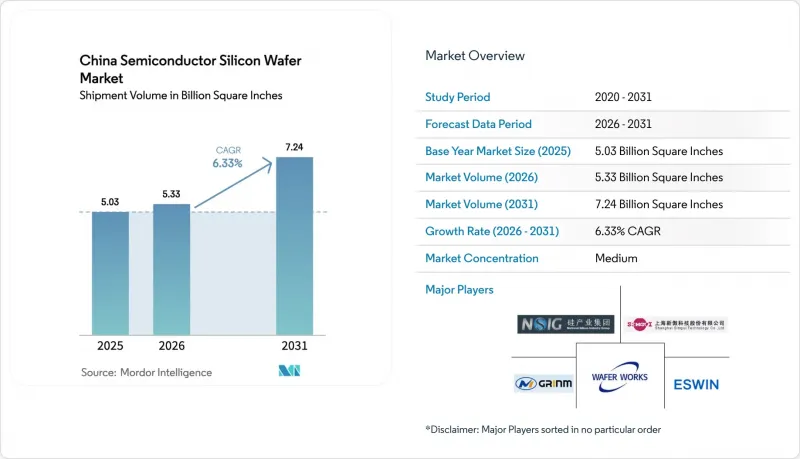
중국의 반도체 실리콘 웨이퍼 시장 출하량 기반 시장 규모는 2025년 50억 3,000만 평방인치로 평가되었습니다. 2026년에는 53억 3,000만 평방인치로 확대되어 2026-2031년에 걸쳐 CAGR 6.33%를 나타내, 2031년까지 72억 4,000만 평방인치에 이를 것으로 예측됩니다.
정부의 강력한 자금 지원, 첨단 해외산 장비에 대한 수출 규제 강화, 현지 파운더리의 생산능력 확대 가속화가 수요를 견인하고 있습니다. 2026년 초부터 시행되고 있는 중국의 '장비 50% 국산화' 의무화에 따라 보조금은 국산 공정 장비 사용과 연계되어 웨이퍼의 추가 주문이 중국 공급업체로 유도되고 있습니다. 로직 및 첨단 아날로그 장치용 12인치 라인의 급속한 도입과 더불어 전기자동차의 보급률 증가로 인해 기판의 총 소비량은 더욱 증가하고 있습니다. 또한, 하이브리드 본딩을 위해 초평탄 프라임 웨이퍼를 필요로 하는 칩렛 기반 AI 가속기의 급증도 시장을 견인하고 있지만, 일본 기존 업체와의 결함 밀도 차이가 여전하여 하이엔드 로직 생산은 일부 수입에 의존하고 있는 상황입니다. 계속되고 있습니다.
중국의 반도체 웨이퍼 시장 동향과 인사이트
국내 제조업체의 300mm 생산능력 급격한 확대
중신국제(SMIC)는 2025년 말, 2026년 말까지 상하이, 베이징, 심천 공장에서월4만 장의 12인치 웨이퍼 생산능력을 추가할 계획을 확정했습니다. 이와 마찬가지로 화홍반도체(HHSC)도 파워 매니지먼트 IC를 대상으로월2만개 추가 생산 계획을 추진하고 있습니다. 각 부처의 토지, 세제, 저금리 융자 혜택은 초기 리스크를 줄이고, 공급업체는 생산 능력을 가동하기 전에 다년 계약(take-or-pay)을 체결할 수 있게 되었습니다. 이에 상하이 실리콘 산업 그룹은 2026년 납품을 위해 임항 공장의 생산 능력을월12인치 웨이퍼 200만 장으로 확대했습니다. 프라임 웨이퍼 한 장당 50달러 이하의 규모의 경제가 전환점이 되어, 이들 대기업과의 비용 경쟁에서 이길 수 없는 소규모 스타트업 기업들 사이에서 통합의 물결이 가속화되고 있습니다.
정부의 '국산 장비 50%' 의무화, 국내 웨이퍼 수요 가속화
2026년 1월부터 산업정보화부는 보조금 지급 조건으로 국산 장비 채택률을 최소 50%로 정하고, 2028년까지 70%까지 끌어올려 2030년에는 완전한 국산화를 목표로 하고 있습니다. 기준을 충족하지 못하는 파운드리는 보조금을 반환해야 하기 때문에 대부분의 기업들은 벤더 리스트를 정리하고 장비와 웨이퍼의 조합을 모두 중국산으로 통일하고 있습니다. Nowra Technologies에 따르면, 28nm 라인에 도입된 증착 장비의 60% 이상이 상하이 실리콘의 웨이퍼와 결합되어 수율 향상 주기를 4분의 1 가까이 단축할 수 있었다고 합니다. 이러한 폐쇄 루프 내에서의 공정 레시피 공유는 결함 제어의 진전을 가속화하고 신규 팹의 학습 곡선을 평탄하게 만듭니다.
28nm 이상 로직 웨이퍼에서 일본 업체와의 결함 밀도 격차가 지속되고 있습니다.
국내산 300mm 프라임 웨이퍼의 평균 결함 밀도는 0.12 결함/cm2로 신에츠케미칼의 벤치마크인 0.08 결함/cm2를 50% 상회하고 있으며, 이는 고급 모바일 프로세서에서 약 8-10%의 수율 저하로 이어집니다. 현지 조달된 폴리실리콘의 0.1ppb를 초과하는 미량 금속 오염이 주요 원인으로 작용하고 있습니다. 파운드리 업체들은 어닐링 시간 연장 및 입고 검사 강화로 이를 보완하고 있으며, 웨이퍼 1장당 15-20달러의 비용 증가가 발생하고 있습니다. 따라서 대량 생산을 하는 팹리스 기업들은 최첨단 로트에 대해 일본산 기판을 지정하고 있으며, 생산 능력의 확대에도 불구하고 국내 공급업체 시장 규모에는 한계가 있습니다.
부문 분석
2025년에는 300mm 카테고리가 전체 출하량의 71.75%를 차지하여 중국의 반도체 실리콘 웨이퍼 시장 점유율의 가장 큰 부분을 차지했고 2031년까지 연평균 복합 성장률(CAGR) 7.16%를 유지할 것으로 예측됩니다. SMIC(Semiconductor Manufacturing International Corporation)에서만월4만 장의 12인치 웨이퍼 생산능력을 추가한 것은 대구경 웨이퍼의 경제성 확보가 불가역적으로 전환되고 있음을 여실히 보여주고 있습니다. 주류 로직 레이아웃에서 300mm 웨이퍼 당 다이 수율은 200mm 웨이퍼의 약 2.5배에 달할 전망입니다. 다이당 원가 절감은 경쟁 칩 가격과 직결되며, 스마트폰과 PC의 교체 주기가 길어지는 상황에서 생존을 위해 필수적인 요소로 작용하고 있습니다.
200mm 부문은 여전히 아날로그 장치 및 실리콘 카바이드(SiC) 장치에 필수적입니다. 전 세계적으로 200mm 공정 장비의 부족으로 인해 리드 타임이 24주까지 늘어났고, 자동차 제조업체들은 다년간의 웨이퍼 공급 계약을 체결해야만 했습니다. 150mm 이하의 웨이퍼는 기존 파워트레인 및 산업용 컨트롤러에 대응하고 있지만, 더 큰 직경으로의 재인증이 불가피함에 따라 그 역할은 종말을 맞이하고 있습니다. 그럼에도 불구하고 중국의 반도체 실리콘 웨이퍼 시장에서 SiC 파워 모듈을 지원하는 6인치 및 8인치 생산 라인에 대한 틈새 예산이 계속 할당되어 주류 300mm 웨이퍼가 직면하고 있는 가격 하락의 영향으로부터 이 부문을 격리시키고 있습니다.
로직용 웨이퍼는 2025년 생산량의 33.37%를 차지했으며, AI 가속기, 엣지 프로세서, 주류 SoC에서의 우위를 반영하고 있습니다. 이 부문의 2031년 CAGR은 6.82%로 메모리 및 아날로그 부문을 능가하는 것으로 나타났습니다. 이는 랙당 수천 개의 고성능 프로세서를 소비하는 국내 AI 클라우드 구축 확대에 따른 것입니다. 따라서 일부 최첨단 다이의 경우 수율 확보를 위해 일본산 웨이퍼를 계속 수입하고 있지만, 로직 용도에 할당되는 중국의 반도체 실리콘 웨이퍼 시장 규모는 확대되고 있습니다.
메모리 웨이퍼의 성장세가 둔화되고 있습니다. 이는 국내 DRAM과 NAND의 생산능력이 여전히 소규모이기 때문입니다. 반면, SiC MOSFET을 중심으로 한 디스크리트 파워 디바이스는 낮은 기저에서 한 자릿수 후반의 높은 성장률을 보이고 있습니다. 아날로그 부문의 성장은 배터리 관리 IC와 자동차용 센싱에 기인한 것이지만, 중국 정부가 '컴퓨팅 주권'을 추진하는 가운데 로직 부문은 여전히 전략적으로 중요한 부문으로 남아 있습니다. 또한, 수요의 다변화로 인해 로직용 웨이퍼 수요는 단일 엔드마켓의 경기 변동에 영향을 덜 받아 전체 소비에서 핵심적인 위치를 확고히 하고 있습니다.
"중국의 반도체 웨이퍼 시장 보고서』는 웨이퍼 직경(150mm 이하, 200mm, 300mm), 반도체 디바이스 유형(로직, 메모리, 기타), 웨이퍼 유형(프라임 폴리싱, 에피택셜, 실리콘 온 인슐레이터(SOI), 특수 실리콘), 최종 사용자(가전, 산업, 자동차, 기타), 지역별로 분류되어 있습니다. 가전용, 산업용, 자동차용, 기타), 지역별로 분류되어 있습니다. 시장 예측은 출하량(평방인치)으로 제공됩니다.
기타 혜택
- 엑셀 형태 시장 예측(ME) 시트
- 3개월간 애널리스트 지원
자주 묻는 질문
목차
제1장 서론
제2장 조사 방법
제3장 주요 요약
제4장 시장 구도
제5장 시장 규모와 성장 예측
제6장 경쟁 구도
제7장 시장 기회와 향후 전망
KTH 26.05.29The China Semiconductor Silicon Wafer Market size in terms of shipment volume is expected to grow from 5.03 Billion Square Inches in 2025 to 5.33 Billion Square Inches in 2026 and is forecast to reach 7.24 Billion Square Inches by 2031 at 6.33% CAGR over 2026-2031.

Robust government funding, tighter export controls on advanced foreign tools, and accelerating capacity additions by local foundries continue to propel demand. Beijing's 50%-domestic-equipment mandate, in force since early 2026, ties subsidies to the use of home-grown process tools, channeling incremental wafer orders toward Chinese suppliers. Rapid adoption of twelve-inch lines for logic and advanced analog devices, combined with rising electric-vehicle penetration, further elevates total substrate consumption. The market also benefits from surging chiplet-based AI accelerators that require ultra-flat prime wafers to enable hybrid bonding, even as lingering defect-density gaps versus Japanese incumbents keep high-end logic output partially import-dependent.
China Semiconductor Silicon Wafer Market Trends and Insights
Surge in 300 mm Capacity Build-Outs by Domestic Players
Semiconductor Manufacturing International Corporation confirmed late-2025 plans to add 40,000 twelve-inch wafer starts each month across Shanghai, Beijing, and Shenzhen fabs by end-2026, a move mirrored by Hua Hong Semiconductor's additional 20,000-wspm program targeting power-management ICs. Provincial incentives in land, taxes, and low-interest loans reduce upfront risk, allowing suppliers to sign multiyear take-or-pay contracts before capacity comes online. Shanghai Silicon Industry Group responded by scaling its Lingang plant to 2 million twelve-inch wafers a month for 2026 delivery. Scale economics below USD 50 per prime wafer become the tipping point, spurring a consolidation wave among smaller startups that cannot reach cost parity with these leaders.
Government "50% Domestic Tool" Mandate Accelerating Local Wafer Demand
Effective January 2026, the Ministry of Industry and Information Technology links subsidies to a minimum 50% local-tool adoption, ratcheting the threshold to 70% by 2028 and full localization in 2030. Foundries that fall short face subsidy claw-backs, so most streamline vendor lists to all-Chinese tool-and-wafer pairings. Naura Technology documented that over 60% of its deposition tools installed on 28 nm lines were matched with Shanghai Silicon substrates, trimming yield-ramp cycles by almost a quarter. Joint process-recipe sharing inside these closed loops accelerates progress on defect control and flattens the learning curve for new fabs.
Persistent Defect-Density Gap Vs. Japanese Suppliers in above 28 nm Logic Wafers
Average defect density of 0.12 defects cm-2 on domestic 300 mm prime wafers remains 50% above Shin-Etsu's 0.08 defects cm-2 benchmark, translating into roughly 8-10% lower yield for advanced mobile processors. Trace-metal contamination above 0.1 ppb in locally sourced polysilicon is a major contributor. Foundries compensate by implementing longer anneals and tighter incoming inspections, adding USD 15-20 per wafer in costs. High-volume fabless customers, therefore, stipulate Japanese substrates for leading-edge lots, capping the market ceiling for domestic suppliers despite capacity growth.
Other drivers and restraints analyzed in the detailed report include:
- Automotive SiC Power Device Boom Driving 200 mm and 8-Inch SiC Wafer Needs
- Rise of Advanced Packaging (Chiplet / X-DFOI) Lifting Demand for Ultra-Flat Prime Wafers
- U.S.-Led Export Controls Limiting Access to Critical CZ Crystal and CMP Tools
For complete list of drivers and restraints, kindly check the Table Of Contents.
Segment Analysis
The 300 mm category accounted for 71.75% of total volume in 2025, capturing the largest slice of the China semiconductor silicon wafer market share and sustaining a 7.16% CAGR through 2031. Capacity additions of 40,000 twelve-inch wafers per month at Semiconductor Manufacturing International Corporation alone underscore an irreversible pivot toward larger-diameter economics, where each 300 mm substrate yields roughly 2.5 times as many die as a 200 mm equivalent for mainstream logic layouts. Cost-per-die savings flow directly into competitive chip pricing, a survival imperative as smartphone and PC refresh cycles extend.
The 200 mm segment remains essential for analog and silicon-carbide devices; global shortages of 200 mm process tools have elevated lead times to 24 weeks, locking automotive customers into multiyear wafer agreements. Sub-150-mm wafers address legacy powertrain and industrial controllers, but face sunset as requalification to larger diameters becomes unavoidable. Nevertheless, the China semiconductor silicon wafer market continues to allocate niche budget to six-inch and eight-inch lines supporting SiC power modules, insulating this pocket from the price erosion afflicting bulk 300 mm primes.
Logic wafers held 33.37% of 2025 volume, reflecting dominance in AI accelerators, edge processors, and mainstream SoCs. The segment's 6.82% CAGR to 2031 outpaces memory and analog, helped by domestic AI cloud build-outs that each consume thousands of high-end processors per rack. The China semiconductor silicon wafer market size allocated to logic applications therefore widens, even though some leading-edge die continue to import Japanese substrates for yield security.
Memory wafers trail because domestic DRAM and NAND capacity is still small, whereas discrete power devices, chiefly SiC MOSFETs, post high-single-digit growth off a low base. Analog growth comes from battery-management ICs and automotive sensing, but logic remains the strategic focus as Beijing presses compute sovereignty. Diversified demand also shields logic wafer offtake from cyclical swings in a single end-market, reinforcing its anchor status within overall consumption.
The China Semiconductor Silicon Wafer Market Report is Segmented by Wafer Diameter (Up To 150 Mm, 200 Mm, 300 Mm), Semiconductor Device Type (Logic, Memory, and More), Wafer Type (Prime Polished, Epitaxial, Silicon-On-Insulator (SOI), Specialty Silicon), End-User (Consumer Electronics, Industrial, Automotive, and More), and Geography. The Market Forecasts are Provided in Terms of Shipment Volume (Square Inches).
List of Companies Covered in this Report:
- National Silicon Industry Group Co. Ltd.
- Shanghai Silicon Industry Group Co. Ltd. (Simgui)
- TCL Zhonghuan Advanced Semiconductor Materials Co. Ltd.
- Hangzhou Lion Microelectronics Co. Ltd.
- Wafer Works (Shanghai) Co. Ltd.
- GRINM Semiconductor Materials Co. Ltd.
- Zhejiang Jinruihong Technologies Co. Ltd.
- Beijing E-SWIN Material Technology Co. Ltd.
- Advanced Semiconductor Manufacturing Corp. (ASM)
- Siltronic AG
- Shin-Etsu Chemical Co. Ltd.
- SUMCO Corp.
- GlobalWafers Co. Ltd.
- SK Siltron Co. Ltd.
- Soitec S.A.
- Ferrotec (Anhui) Technology Co. Ltd.
- Hangzhou Semiconductor Wafer Co. Ltd.
- Hebei Puxing Semiconductor
- Chongqing Advanced Silicon Technology
- Nanjing Guosheng Electronics
Additional Benefits:
- The market estimate (ME) sheet in Excel format
- 3 months of analyst support
TABLE OF CONTENTS
1 INTRODUCTION
- 1.1 Study Assumptions and Market Definition
- 1.2 Scope of the Study
2 RESEARCH METHODOLOGY
3 EXECUTIVE SUMMARY
4 MARKET LANDSCAPE
- 4.1 Market Overview
- 4.2 Market Drivers
- 4.2.1 Surge in 300 mm Capacity Build-outs by Domestic Players
- 4.2.2 Government "50 % Domestic Tool" Mandate Accelerating Local Wafer Demand
- 4.2.3 Automotive SiC Power Device Boom Driving 200 mm and 8-inch SiC Wafer Needs
- 4.2.4 Tight Global 200 mm Tool Supply Forcing Chinese Fabs to Lock-in Local Wafer Supply
- 4.2.5 Subsidized Polysilicon Price Support Enhancing Cost Advantage
- 4.2.6 Rise of Advanced Packaging (Chiplet / X-DFOI) Lifting Demand for Ultra-Flat Prime Wafers
- 4.3 Market Restraints
- 4.3.1 Persistent Defect-Density Gap vs. Japanese Suppliers in above 28 nm Logic Wafers
- 4.3.2 U.S.-Led Export Controls Limiting Access to Critical CZ Crystal and CMP Tools
- 4.3.3 Margin Pressure from Mature-Node Over-Capacity and Price-War Among Foundries
- 4.3.4 Skills Shortage in Ultra-Pure Water and Chemical Waste Treatment Operations
- 4.4 Industry Value-Chain Analysis
- 4.5 Technology Analysis
- 4.6 Regulatory Landscape
- 4.7 Impact of Macroeconomic Factors
- 4.8 Porter's Five Forces Analysis
- 4.8.1 Bargaining Power of Suppliers
- 4.8.2 Bargaining Power of Buyers
- 4.8.3 Threat of New Entrants
- 4.8.4 Threat of Substitutes
- 4.8.5 Intensity of Competitive Rivalry
5 MARKET SIZE AND GROWTH FORECASTS (VOLUME)
- 5.1 By Wafer Diameter
- 5.1.1 Up to 150 mm
- 5.1.2 200 mm
- 5.1.3 300 mm
- 5.2 By Semiconductor Device Type
- 5.2.1 Logic
- 5.2.2 Memory
- 5.2.3 Analog
- 5.2.4 Discrete
- 5.2.5 Other Semiconductor Device Types (Optoelectronics, Sensors, Micro)
- 5.3 By Wafer Type
- 5.3.1 Prime Polished
- 5.3.2 Epitaxial
- 5.3.3 Silicon-on-Insulator (SOI)
- 5.3.4 Specialty Silicon (High-Resistivity, Power, Sensor-Grade)
- 5.4 By End-user
- 5.4.1 Consumer Electronics
- 5.4.1.1 Mobile and Smartphones
- 5.4.1.2 PCs and Servers
- 5.4.2 Industrial
- 5.4.3 Telecommunications
- 5.4.4 Automotive
- 5.4.5 Other End-user Applications
- 5.4.1 Consumer Electronics
6 COMPETITIVE LANDSCAPE
- 6.1 Market Concentration
- 6.2 Strategic Moves
- 6.3 Market Share Analysis
- 6.4 Company Profiles (includes Global Level Overview, Market Level Overview, Core Segments, Financials as available, Strategic Information, Market Rank/Share, Products and Services, Recent Developments)
- 6.4.1 National Silicon Industry Group Co. Ltd.
- 6.4.2 Shanghai Silicon Industry Group Co. Ltd. (Simgui)
- 6.4.3 TCL Zhonghuan Advanced Semiconductor Materials Co. Ltd.
- 6.4.4 Hangzhou Lion Microelectronics Co. Ltd.
- 6.4.5 Wafer Works (Shanghai) Co. Ltd.
- 6.4.6 GRINM Semiconductor Materials Co. Ltd.
- 6.4.7 Zhejiang Jinruihong Technologies Co. Ltd.
- 6.4.8 Beijing E-SWIN Material Technology Co. Ltd.
- 6.4.9 Advanced Semiconductor Manufacturing Corp. (ASM)
- 6.4.10 Siltronic AG
- 6.4.11 Shin-Etsu Chemical Co. Ltd.
- 6.4.12 SUMCO Corp.
- 6.4.13 GlobalWafers Co. Ltd.
- 6.4.14 SK Siltron Co. Ltd.
- 6.4.15 Soitec S.A.
- 6.4.16 Ferrotec (Anhui) Technology Co. Ltd.
- 6.4.17 Hangzhou Semiconductor Wafer Co. Ltd.
- 6.4.18 Hebei Puxing Semiconductor
- 6.4.19 Chongqing Advanced Silicon Technology
- 6.4.20 Nanjing Guosheng Electronics
7 MARKET OPPORTUNITIES AND FUTURE OUTLOOK
- 7.1 White-Space and Unmet-Need Assessment
